Article

Bifurcation Phenomena in Open-Loop DCM-Operated DC–DC Switching Converters Feeding Constant Power Loads

1
Department of Electronics, Electrical Engineering and Automatic Control, Universitat Rovira i Virgili, 43002 Tarragona, Spain
2
Department of Physics, Universitat Politècnica de Catalunya, 08034 Barcelona, Spain
3
Department of Electrical Engineering Hong Kong, City University of Hong Kong, Hong Kong, China
*
Author to whom correspondence should be addressed.
Electronics 2023, 12(4), 1030; https://doi.org/10.3390/electronics12041030
Submission received: 17 January 2023 / Revised: 15 February 2023 / Accepted: 16 February 2023 / Published: 19 February 2023
(This article belongs to the Special Issue Design and Applications of Nonlinear Circuits and Systems)

Abstract

:
Constant power loading is an effect that appears in multiple-stage energy conversion systems with individually regulated switching power converters. In a two-stage system, an upstream or source converter drives one or more downstream or load converters. The downstream converters in a two-stage power conversion system are designed to provide the fastest transient response in stand-alone operation. Consequently, they behave as a constant power load (CPL) to the upstream converter within their control bandwidth. In the past, open-loop power converters feeding CPLs and operating in discontinuous conduction mode (DCM) were considered to be stable. In this paper, it is shown that these systems can undergo instabilities, which have been so far overlooked. First, numerical simulations from the switched model of an open-loop boost converter under DCM operation and loaded with a tightly regulated buck converter and the same converter loaded by an ideal CPL are presented to show that they exhibit similar nonlinear behavior and bifurcation phenomena. Then, the three elementary open-loop DC–DC converters operating in the DCM were considered and their bifurcation phenomena were revealed. It is shown that the period-doubling route to chaos in the DC–DC boost converter is interrupted by a sudden appearance of dangerous destructive dynamics due to the excessively unlimited load current in the CPL. For the buck converter, only the first period-doubling bifurcation is observed before the destructive behavior appears. The open-loop buck–boost converter under DCM and feeding a CPL is always unstable and exhibits no periodic orbit. Based on the observed phenomena, approximate discrete-time models were derived, which despite their simplicity, were seen to display the most-important and -essential features of the corresponding switching converters before destructive dynamics occurs.

1. Introduction

Cascaded DC–DC power converters appear in many engineering applications of power electronics such as electric vehicles and ships [1,2,3,4,5], microgrids [6,7,8,9], more electric power aircraft [10], and more electric ships [4], among others. In cascaded DC–DC converters, the first stage is called the source or the upstream converter, and the second stage is the load or the downstream converter. When the latter is controlled to maintain a tightly regulated output voltage on the load, it behaves as a constant power load (CPL) for the source converter [9,10,11,12,13,14]. For instance, in a microgrid with different voltage buses, if the downstream power electronics interface, which could be a grid-connected DC–AC inverter or a DC–DC converter, is tightly regulated, it will absorb constant power from the upstream DC–DC converter. The motor of an electric vehicle (EV) with tight velocity control and under constant torque operation will also absorb constant mechanical power from the three-phase DC–AC inverter, hence resulting in a CPL to the upstream DC–DC boost converter [14]. It is remarkable that the source converters in the previously mentioned applications feed CPLs and that the number of these applications is increasing at an enormous rate.
A DC–DC converter comprises reactive elements such as inductors and capacitors and semiconductor devices such as transistors and diodes operating as periodically controlled switches that change their state when certain events take place. The common node between the transistor and the diode connects to an inductor. In most of the applications, continuous conduction mode (CCM) is employed. In this case, the inductor current never drops to zero. Yet, discontinuous conduction mode (DCM) can also be used for certain applications. In this case, the inductor current drops to zero and remains null until the end of the switching cycle. When a converter operates in DCM, it provides the potential advantages of better closed-loop stability with simple control and the reduced cost of the converter, among others advantages [15]. DCM typically occurs with a large inductor current ripple in a unidirectional converter operating at a light load. For instance, DCM is eventually encountered in a converter when its load is removed. In some applications, converters are deliberately designed to operate in DCM for all loading conditions. The DCM operation of elementary DC–DC converters is characterized by the fact that some switching instants are internally controlled even under open-loop operation. Indeed, the diode changes its conducting state when the inductor current becomes zero.
Generally, the mathematical model of cascaded DC–DC converters is high-dimensional, making their stability analysis challenging. The impedance criterion is a frequency domain technique widely used for the stability analysis of cascaded converters, after it was first proposed for predicting input filter interactions in DC–DC converters [16]. Later, the same criterion was applied for cascaded converters, leading to the definition of the minor loop gain consisting of the ratio between the output impedance Z o of the load converter and the input impedance Z i of the source or downstream converter. This minor loop Z o / Z i has since been widely used to assess the stability of cascaded converters.
In the theoretical treatment of the instabilities of the full-order system, several idealizations of the actual features of its behavior are possible. The choice of the idealization to be made and the parameters and the state variables to be omitted or simplified in the mathematical model depend on the specific problem and the kind of instability to be studied. The usual idealization of the load converter is to consider it as a CPL, leading naturally to a static equation for this stage, hence to a significant order reduction of the source converter model, but at the expense of an additional nonlinearity in the state equations. Indeed, in this kind of application, the whole system can be simplified as a DC–DC converter supplying a nonlinear CPL [9,14]. The effect of the different parameters of the source converter from the perspective of its stability can be, therefore, revealed using reduced-order models.
In reality, the steady-state regime of DC–DC converters is a periodic orbit, not an equilibrium point. The desired period of this periodic orbit is the same period of the external driving signal of the switches [17,18,19]. In the past, current-mode-controlled DC–DC converters have been a subject of intensive research studies (see [19] and the references therein), where it was shown using bifurcation theory that these systems are prone to exhibit a rich variety of complex dynamics and nonlinear behavior such as subharmonic and chaotic oscillations. The coexistence of different steady-state behaviors has been also shown to occur in these systems. Another type of bifurcation mainly attributed to the discontinuity of their Poincaré map models has been also demonstrated to take place in DC–DC converters. These discontinuity-induced phenomena are called border collision bifurcations [18]. In this type of bifurcation, the standard cascade period-doubling scenario is interrupted by a sudden jump to a different behavior due to the collision of the system trajectory or limit cycle with a border defining the limit of validity of the converter model.
Close to an operating point, CPLs exhibit a negative resistance behavior, leading to a high risk of instability [11,14,20,21]. A large number of different analysis attempts have been published for the converters feeding CPLs and operating in CCM, but only a few of these converters operating in DCM have been addressed. From the existing literature, it can be claimed that, with the exception of [22,23], the research and results that have been published so far on the instability issues in DC–DC converters feeding CPLs considered the CCM operation. The available results on the stability analysis in [22,23] were based on averaged models, leading to inaccuracies in predicting the onset of instability in these systems in the parameter space. Indeed, it was concluded in [23] that the open-loop buck and boost converters operating in DCM are stable when they are loaded by CPLs. Using a nonlinear implicit discrete-time model [17,24,25,26,27,28], we show here that such claims about the stability of the buck and the boost converter are not accurate.
It is well known that closed-loop switching converters with both resistive loads and CPLs are prone to exhibit a large variety of complex dynamics and undesired instabilities [18,19,29,30,31,32,33,34,35,36,37]. The common denominator in all the past studies and research works was the consideration of a closed-loop converter either under VMC [17,26,27,28,38,39,40,41] or current mode control (CMC) [42,43,44,45,46,47]. In converters with a linear load, either resistive [17,26,27,28,38,40] or constant current [41] load, the piecewise linear state equations are employed for DC–DC converters to obtain the discrete-time model, and the stability analysis passes through solving the eigenvalues problem of the Jacobian matrix of this model, which can be obtained in closed-form. This is not directly applicable to DC–DC converters loaded by a CPL [30,31]. To effectively study instabilities in this case, ad hoc stability analysis techniques must be used. For instance, the piecewise linear approach can still be be employed to obtain their approximate discrete-time model and to perform the stability analysis of their periodic orbits, but after a careful linearization of the nonlinear model of the CPL [31].
For DC–DC converters with a resistive load operating in DCM and under a VMC feedback loop intending to regulate the output voltage, approximated discrete-time models were used in [38,39] to predict the onset of period-doubling bifurcation. The approximate discrete-time models were obtained by approximating the state transition matrices corresponding to each switch position of the converters. The same model can be obtained by discretizing the averaged model at the switching frequency rate. This is particularly useful when the state transition matrices are not available in closed-form, as when the load is nonlinear, such as a CPL. The model used in [38,39] was re-utilized in [48] to study the small signal behavior of a DC–DC converter. It is worth noting that, in the previous work, open-loop operated converters were not considered. Obviously, with a linear resistive load, the discrete-time model corresponding to an open-loop DC–DC converter is linear and always stable, and therefore, bifurcation phenomena cannot take place. The situation is different when the load is nonlinear, as the one considered in this study. In this case, the discrete-time model of the converter is nonlinear even under open-loop operation, and bifurcation phenomena can take place, as will be detailed later.
The main novelty in this paper is that the nonlinear behavior was observed in DC–DC converters operating in open-loop, i.e., with a duty cycle given in a fixed pattern and without any feedback loop. Apart from [49], which was our initial work on this topic, the literature reports no other work on nonlinear behavior such as period-doubling and bifurcation phenomena in open-loop-operated DC–DC converters. Indeed, an accurate implicit discrete-time modeling approach was proposed in [49], where the dynamics of the open-loop boost converter operating in DCM and feeding a CPL was explored in the parameter space, revealing the occurrence of period-doubling bifurcation when suitable parameters were varied. Following our previous work in [49] for the boost converter, we extended here our study to other elementary switching converters. The three open-loop elementary DC–DC converters feeding CPLs were considered and their stability analysis performed. Approximate explicit discrete-time models for the buck and the boost were also derived, allowing us to analytically perform the stability at the fast switching scale, predicting the onset of period-doubling and other bifurcations in the parametric space. The derived models, despite their simplicity, were to display the most-important and -essential features of the corresponding switching converters.
The rest of this paper is organized as follows: After this Introduction, in Section 2, the dynamical behavior of a DC–DC boost converter loaded by a CPL and operating in DCM is compared to the behavior of the same converter loaded by a tightly regulated buck converter, putting in evidence the CPL effect of the latter. The experimental setup and some measurements are presented in Section 3, showing period-doubling bifurcation in an open-loop-DCM-operated boost converter with a CPL. The switched models of the three elementary DC–DC converters loaded by a CPL are given in Section 4, and the parametric space region where they operate in DCM is determined in Section 5 in tabular form. In Section 6, the average dynamics for DCM-operated power converters loaded by a CPL are given, and the expression of their equilibrium points, static voltage conversion gains, and stability boundary at the slow time scale (low-frequency) are determined. In Section 7, the period-doubling bifurcation of periodic orbits in open-loop-DCM-operated DC–DC converters feeding CPLs are shown to occur in these systems by using numerical simulations performed on the exact switched model implemented in the PSIM© software. The nonlinear dynamic behavior is addressed in Section 8, where the existence conditions and the stability and bifurcation analysis of the fundamental one-periodic orbit are presented, and different regions in the parameter space are determined for the open-loop boost and the buck converters. Finally, Section 9 summarizes the conclusions of this work.

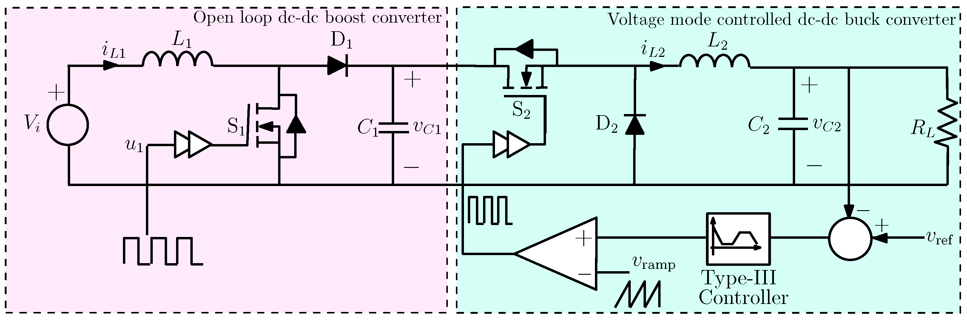
2. Period-Doubling Bifurcation in an Open-Loop DCM-Operated Boost Converter Feeding a Tightly Regulated Buck Converter
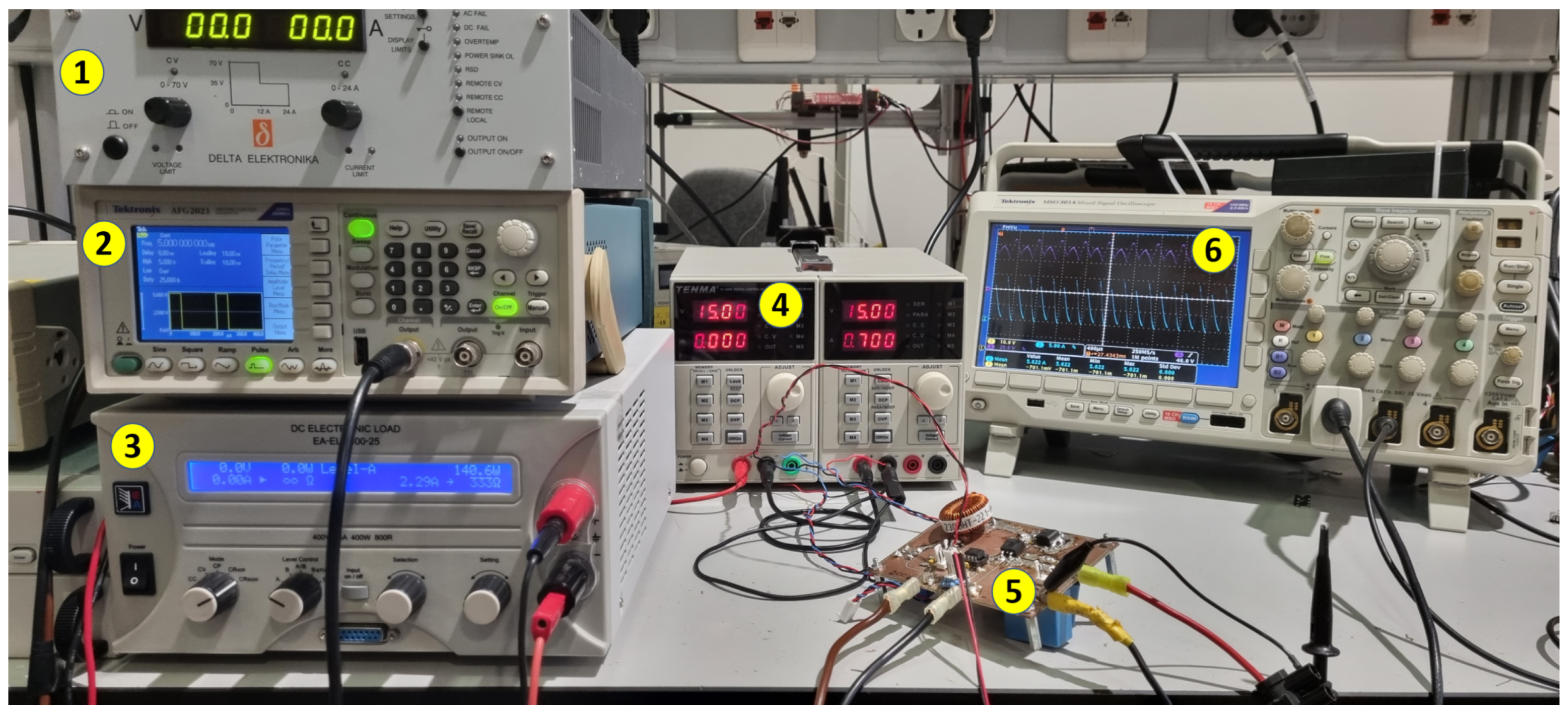
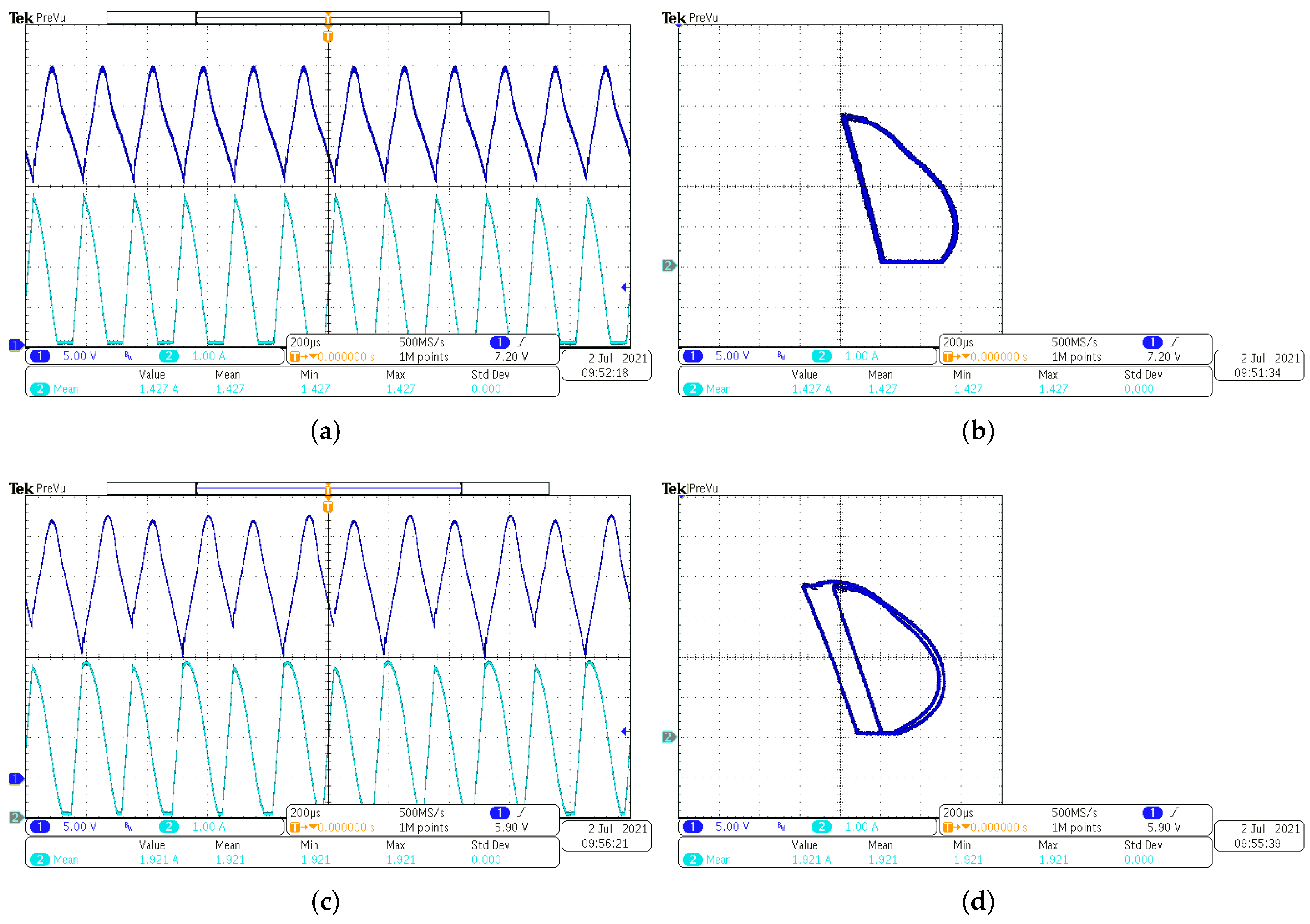
The CPL effect was retaken here for a cascaded connection of two converters being the source converter operating in open-loop and under DCM and the load converter under a tight control of the output voltage. As an example, we considered here an open-loop boost converter loaded by a voltage-mode-controlled buck converter using a two-zero three-pole Type-III controller, as illustrated in Figure 1. Notice that, traditionally, converters with tight voltage control using a fixed frequency PWM are considered as a CPL [1,2]. Since the power delivered to the load is proportional to the squared voltage, if the voltage is tightly regulated, the instantaneous absorbed power will be practically constant. The values of the circuit parameters for the source converter and the load converters are depicted in Table 1. The chosen parameter values of the boost converter guarantee DCM operation. Those of the buck converter power stage and its operating duty cycle (output voltage) correspond to CCM. The parameter values of the Type-III voltage controller were chosen for an optimal response in terms of bandwidth and overshoot. For that, the gain of the controller was κ = 0.6 , the two zeros’ frequencies were 1 kHz and 8 kHz, and the two poles’ frequency was 50 kHz both. The buck converter was loaded by a resistive load, whose resistance R L was varied according to the power of the CPL ( P = v ref 2 / R L ).
Figure 2 shows the behavior of an open-loop boost converter operating in DCM loaded, in the first case, by a tightly regulated buck converter with VMC and, in the second case, by an ideal CPL with the load power corresponding to a stable periodic regime and subharmonic oscillation in both cases. The agreement between the results depicted in Figure 2 was remarkable. Therefore, we continued our study by considering the load converter as an ideal CPL.

3. Experiments

An experimental prototype was used to observe some of the nonlinear phenomena considered in this study. A picture of the experimental setup is shown in Figure 3.
A dynamic load, ELEKTRO-AUTOMATIK EL3400-25, was used to emulate a CPL as a load for the converter. The nominal values of parameters were the same ones used in the theoretical study that will be presented. The switch was implemented using the IPB60R099CPA CoolMOS, and the used diode was STTH30R06CW (a Schottky diode). The inductor was fabricated using the Toroidal Magnetics Kool-mu core 2300HT-220-V-R with a nominal value of 200 μH. Its internal resistance was measured to be approximately 0.1 Ω. The output capacitor used consisted of a parallel connection of three film capacitors with a capacitance of 1.5 μF for each one, for a total capacitance of 4.5 μF. The driving square wave signal for the switch was provided by a function generator, Tektronix AFG2021. The switching frequency was fixed to 5 kHz, and its duty cycle was fixed to 0.22. The input voltage was fixed to 48 V. All the measurements were captured using a TEKTRONIX oscilloscope, MDO 3024.
Figure 4 shows the time domain waveforms and the state plane trajectories for two different values of the power. For P = 28 W, the system behavior was stable and periodic with the same period as the driving signal (Figure 4a,b). For P = 30 W, the converter exhibited subharmonic oscillation due to a period-doubling bifurcation (Figure 4c,d).
Remark 1.
Due to the danger of experimenting with a CPL because of the destructive dynamics associated with the small CPL voltage and, consequently, unlimited current, the values of the power used were deliberately chosen to be low in the experiments. However, the same phenomena take place for higher values of the power, but this could result in a dangerous catastrophic destructive behavior for the converter and also the electronic load emulating the CPL. Our main concern in this paper was to demonstrate that period-doubling bifurcation is possible in an open-loop-operated DC–DC converter when this is loaded by a CPL. Observe that, under complex dynamics, such as subharmonic oscillation and chaotic regimes, the ripple of the state variables becomes so large, that if the voltage of the CPL approaches low values, its current becomes very large, and vice versa, if the current approaches very small values, the voltage becomes very high. In both cases, once the current or the voltage reaches a certain value, the protections of the electronic load that we used to emulate the CPL are activated. With the protections activated, the dynamics of the system change, and some phenomena such as chaotic behavior would not be possible to detect.

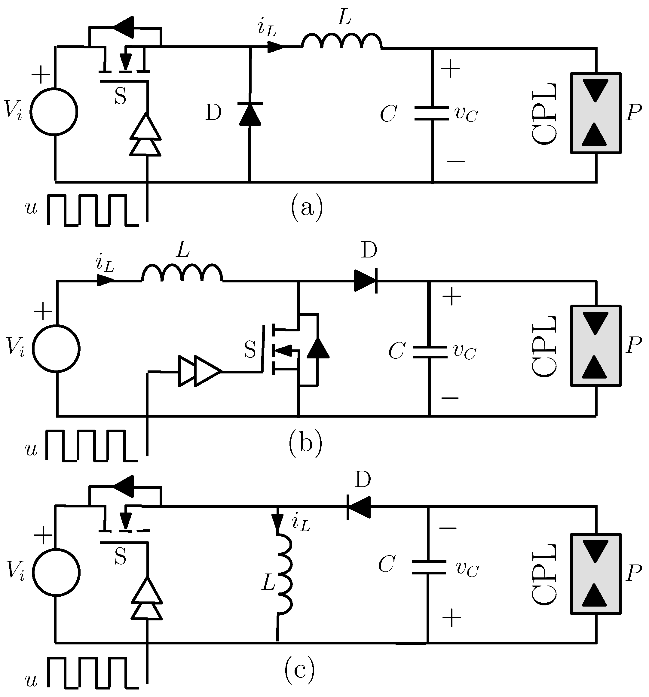
4. Switched Model of Open-Loop Elementary DC–DC Switching Converters with a CPL

The theoretical study carried out in this paper corresponded to the elementary buck, boost, and buck–boost converters loaded by a CPL depicted in Figure 5. It was supposed that the switch Q of the converter is driven by a square wave periodic signal u with a period T (switching frequency f s = 1 / T ) and a fixed duty cycle D ( 0 , 1 ) . Table 2 summarizes the state equations of three elementary converters with physical state variables and parameters, where v C is the voltage across the capacitor, whose capacitance is C, i L is the current through the inductor, whose inductance is L, V i is the input voltage, and P is the CPL power.

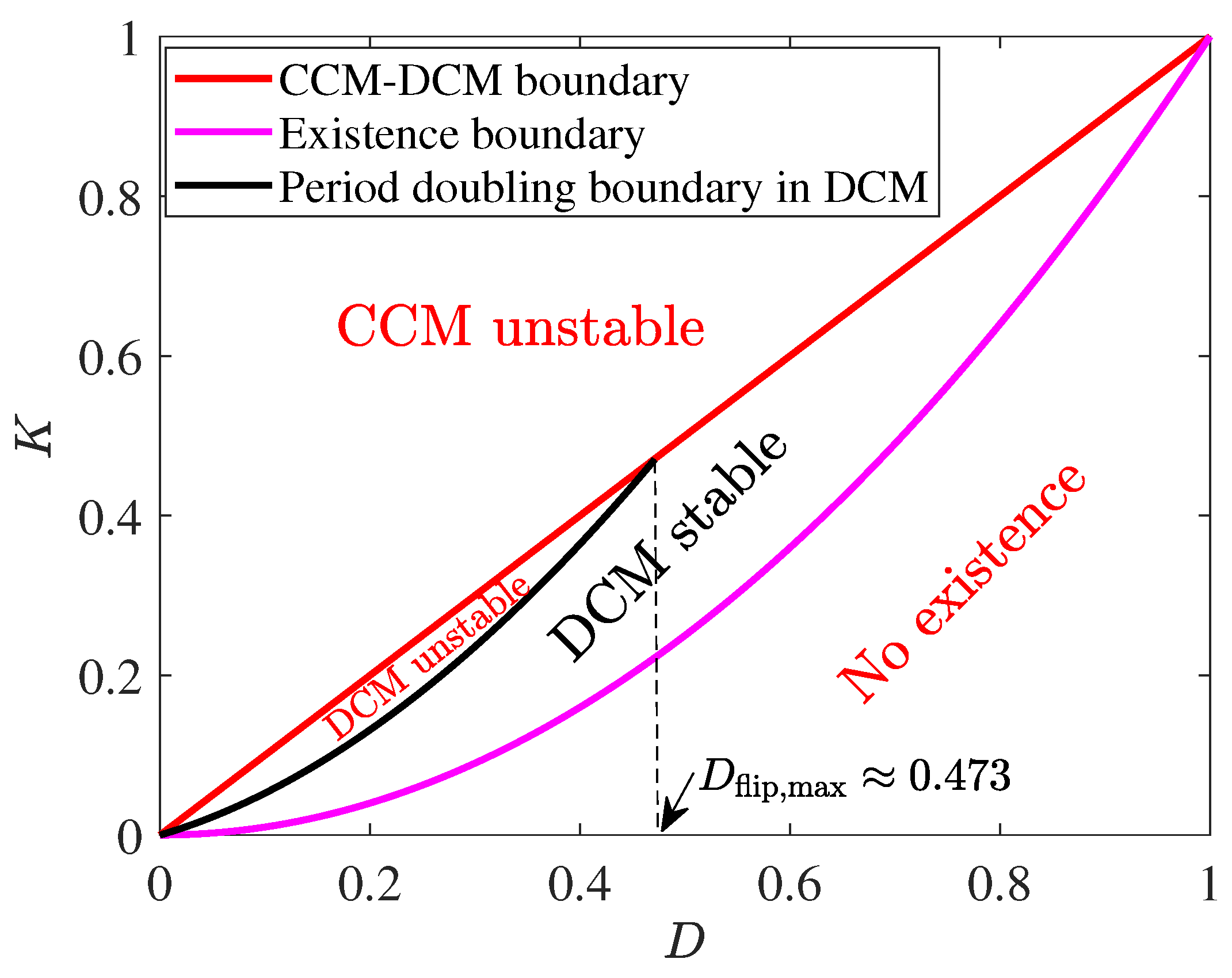
5. Parametric Space Region for DCM Operation

As in the resistive load case, the boundary between the CCM and DCM operation can be derived in terms of the switching period T, inductance value L, duty cycle D, and input voltage V i . In the case of the CPL, the boundary also depends on the constant power P. The analysis reported in [50] (Chap. 5) was here adapted for the case of a CPL. In the boundary between CCM and DCM, the inductor current i L of any elementary converter behaves in steady-state, as illustrated in Figure 6. Roughly speaking, the operation in DCM will eventually take place if either the ripple Δ i L is increased or the average inductor current I L is decreased. The expression of I L is given in Table 3 for the three elementary converters. At the boundary of CCM–DCM, one has Δ i L = 2 I L = I p .
By particularizing the previous condition for the three elementary converters, the expressions shown in Table 3 for the critical value P cri of the power P were obtained for the three elementary converters. The converter will work in DCM if P < P cri . Let us define the dimensionless parameter K = 2 L P / ( V i 2 T ) . In terms of this dimensionless parameter, the CCM–DCM boundary conditions for the three elementary converters can be rewritten as K = K cri ( D ) , where K cri ( D ) is given Table 3. Figure 7 shows the CCM–DCM boundary for the three elementary switching converters with a CPL in the dimensionless parameter space ( D , K ) . For a specific value of D, if K > K cri ( D ) , CCM takes place, and if K < K cri ( D ) , DCM occurs.
It is worth noting that, for the buck converter, the maximum value of K cri ( D ) is 4 / 27 . This maximum value occurs for D = 2 / 3 . Therefore, for this converter, the DCM operation will not take place for no value of D if K > 4 / 27 . For the boost and the buck–boost converter, there will always exist an interval of the operating duty cycle D within which the DCM operation will theoretically take place if K < 1 . This interval becomes wider if the value of the dimensionless parameter K decreases.

6. Average Dynamics for DCM-Operated Power Converter with a CPL: Equilibrium Point, Static Voltage Conversion Gain, and Stability

6.1. Averaged Model

Under certain conditions, the dynamics of a DCM-operated converter can be accurately described by an averaged model. Let us assume that the capacitor voltage v C ripple is sufficiently small during a switching cycle such that time dependence of the inductor current i L can be considered linear: i L goes from 0 to a certain peak value I p during the time interval ( 0 , D T ) (that for u = 1 ); after that, i L drops to 0 during the time interval ( D T , ( D + D ) T ) and remains 0 during the rest of the period with duration ( 1 D D ) T (Figure 8).
From the expression of the inductor current time derivative d i L / d t in Table 2 with u = 1 , the peak inductor current I p was obtained, and from the same equation with u = 0 , one obtain the expression of the ratio D . These results are summarized in Table 4, and using them in the capacitor voltage derivative d v C / d t (Table 2), in which i L in the buck is substituted by its average ( D + D ) I p / 2 and ( 1 u ) i L in the boost and buck–boost is substituted by D I p / 2 , the following averaged models are obtained:
d v ¯ C d t = P C v ¯ C V i v ¯ C V i D 2 K 1 buck
d v ¯ C d t = P C v ¯ C v ¯ C v ¯ C V i D 2 K 1 boost
d v ¯ C d t = P C v ¯ C D 2 K 1 buck - boost
where the overline stands for averaging over one switching period, i.e., v ¯ C ( t ) = t t + T v C ( τ ) d τ . It is worth noting that the previous models are nonlinear with respect to both the average state variable v ¯ C and the duty cycle D. Note also that, in order, to guarantee the DCM operation, the condition D + D < 1 must hold; thus, the value of K cri in Table 3 can also be obtained from this condition with D and v ¯ C = V C (steady-state) given in Table 4.

6.2. Equilibrium Points

In the case of existence, the equilibrium points can be obtained by making d v ¯ C / d t = 0 in the previous differential equations, hence obtaining the expressions of V C shown in Table 4 for the buck and the boost converters, while no equilibrium exists for the DCM-operated buck–boost converter with a CPL. Note that, for the equilibrium point to exist in the buck and the boost converters, the conditions K < D 2 and K > D 2 must be fulfilled, respectively. Note also that D 2 < D 2 ( 1 D ) , D ( 0 , 1 ) , and therefore, an equilibrium point always exists for the buck converter provided that it operates in DCM ( K < K cri : = D 2 ( 1 D ) ).

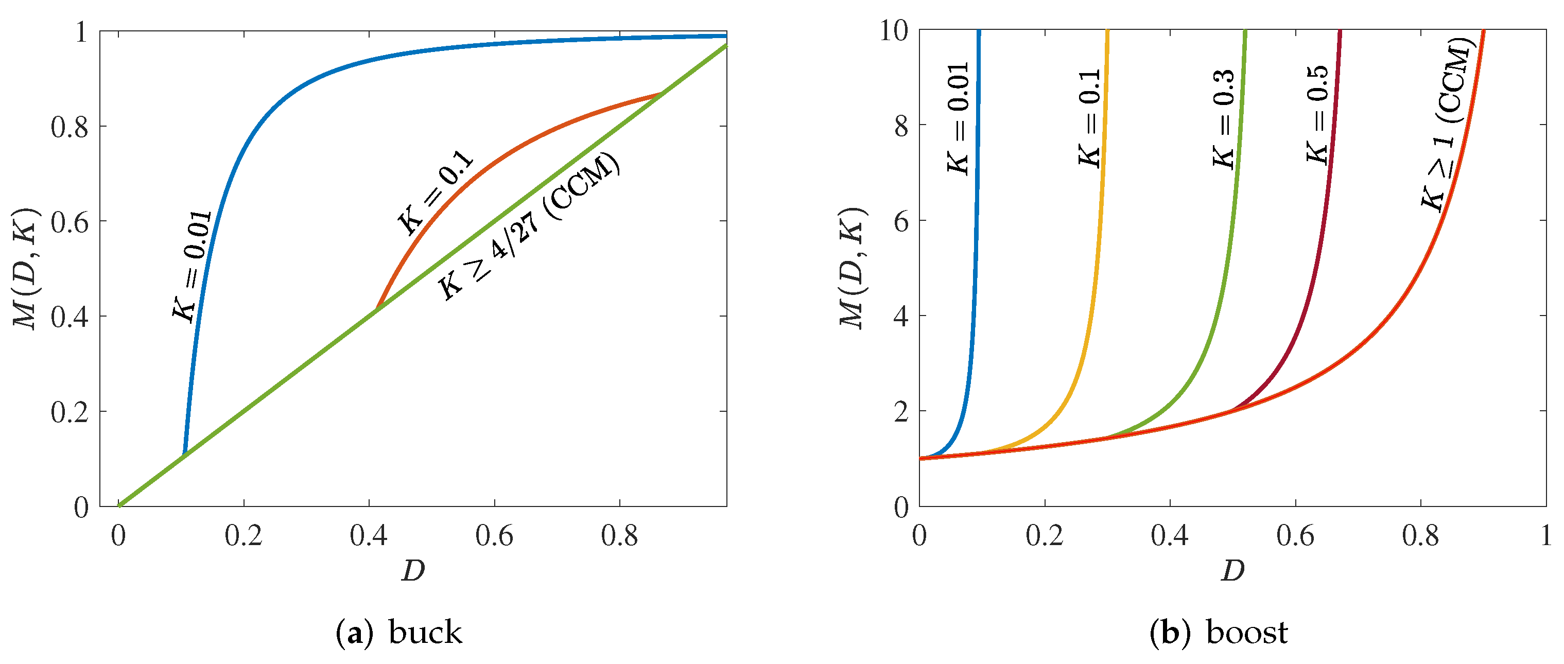
6.3. Conversion Ratio

Under the existence conditions, the voltage conversion gain M ( D , K ) : = V C / V i for the DCM-operated buck and the boost converters with a CPL are given in Table 4. These conversion ratios are plotted in Figure 9 in terms of the duty cycle D for different values of K. It is worth noting that, at the boundary between CCM and DCM, the conversion ratios become the widely known load-independent voltage gains M ( D ) = D and M ( D ) = 1 / ( 1 D ) for the buck and the boost converters, respectively.
As stated before, the DCM-operated open-loop buck–boost converter does not have an equilibrium point. Indeed, the solution of its averaged differential Equation (3) can be obtained in closed-form, and it confirms the previous statement. Let z ( t ) = 1 2 C v ¯ C 2 , that is the averaged stored energy in the capacitor. Therefore, from (3), one obtains the following differential equation corresponding to the buck–boost converter in terms of z.
d z d t = P D 2 K 1
whose solution is as follows:
z ( t ) = z ( 0 ) + P D 2 K 1 t
Equivalently, in terms of the averaged value v ¯ C , one has
v ¯ C ( t ) = v ¯ C 2 ( 0 ) + 2 P C D 2 K 1 t
Three different cases arise depending on D 2 and K. These are:
  • K < D 2 (DCM operation): The response does not reach any equilibrium in steady-state. It is unbounded, and the system is unstable.
  • K = D 2 (CCM–DCM boundary): The response is bounded, but presents an infinite number of equilibria depending on the initial condition v C ( 0 ) . Indeed, in this case, one has v C ( t ) = v C ( 0 ) t .
  • K > D 2 (CCM operation): The response collapses at a certain time instant t c given by
    t c = C v ¯ C 2 ( 0 ) 2 P K ( K D 2 )
At this time instant, the voltage v C across the CPL becomes zero and the current through it becomes infinite. For t > t c , no real solution exists for the buck–boost converter averaged state equation. A similar treatment can be made for the buck and the boost converters under the conditions V i v ¯ C and V i v ¯ C , respectively, but in general, the average state equations of these two converters cannot be integrated in closed-form.
Remark 2.
A so-called fast instability was reported in [20], where it was stated that, based on the system parameter values, the converter can go to instability very fast and it does not have enough time even to change the status of the switch. In that work, a resistive load was added in parallel with the CPL in the buck–boost converter for an equilibrium point to exist. In reality, this phenomenon takes place because either the initial condition is selected out of the basin of attraction of the equilibrium point or the latter does not exist, provoking a voltage collapse to zero and an infinite current through the CPL. In the experimental circuit, this dangerous catastrophic destructive dynamics may lead to the destruction of switching devices.
Remark 3.
The previous remark is based on the averaged model of the converters. In the real switched system, the ripple of the state variables either in periodic, subharmonic, or chaotic regimes may make voltage collapse to take place at a time instant smaller than t c .

6.4. Stability at the Low Frequency (Slow Scale)

To perform the stability analysis of the equilibrium point of the buck and the boost converters, let us define the error e : = v ¯ C V ¯ C . Therefore, from (1) and (2), one can write
d e d t = φ ( v ¯ C )
where φ ( v ¯ C ) is the following function:
φ ( v ¯ C ) = P C V i v ¯ C D 2 K buck
φ ( v ¯ C ) = P C ( v ¯ C V i ) v ¯ C 1 D 2 K boost
Let us consider the Lyapunov function candidate V = e 2 / 2 . Its time derivative is d V / d t = e d e / d t = φ ( v ¯ C ) e 2 . For the buck converter, φ ( v ¯ C ) is always negative, and the equilibrium point is unconditionally stable since the time derivative of the Lyapunov function is negative in this case. For the boost converter, under the existence condition of the equilibrium point ( D 2 < K ) and if the condition v ¯ C > V i is guaranteed, φ ( v ¯ C ) will be negative, and the error asymptotically vanishes in this case.

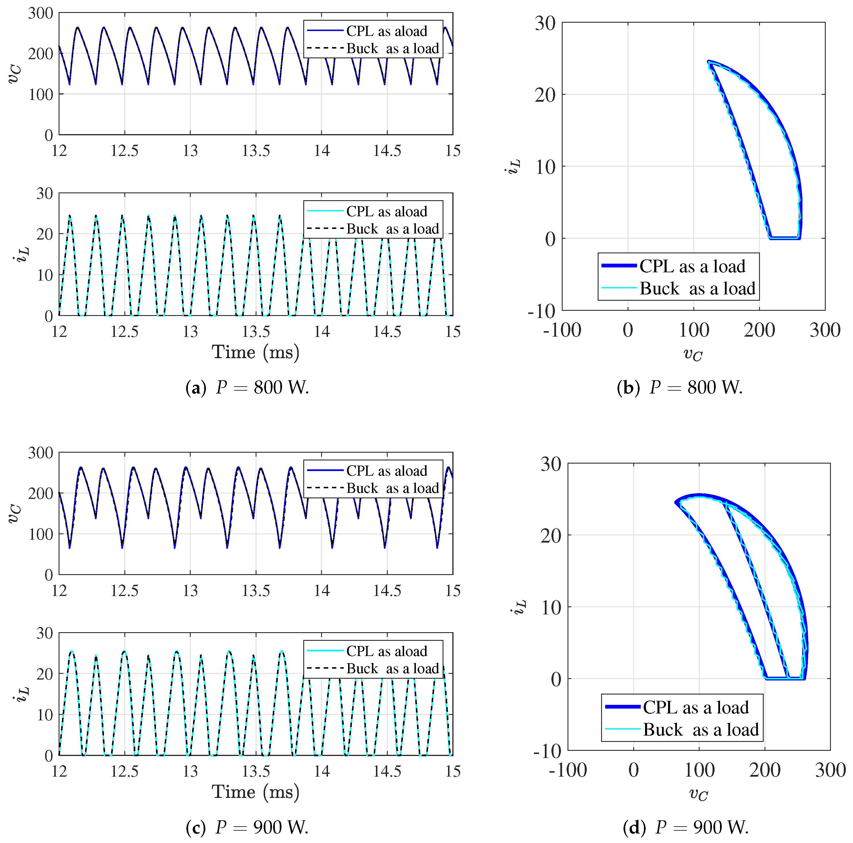
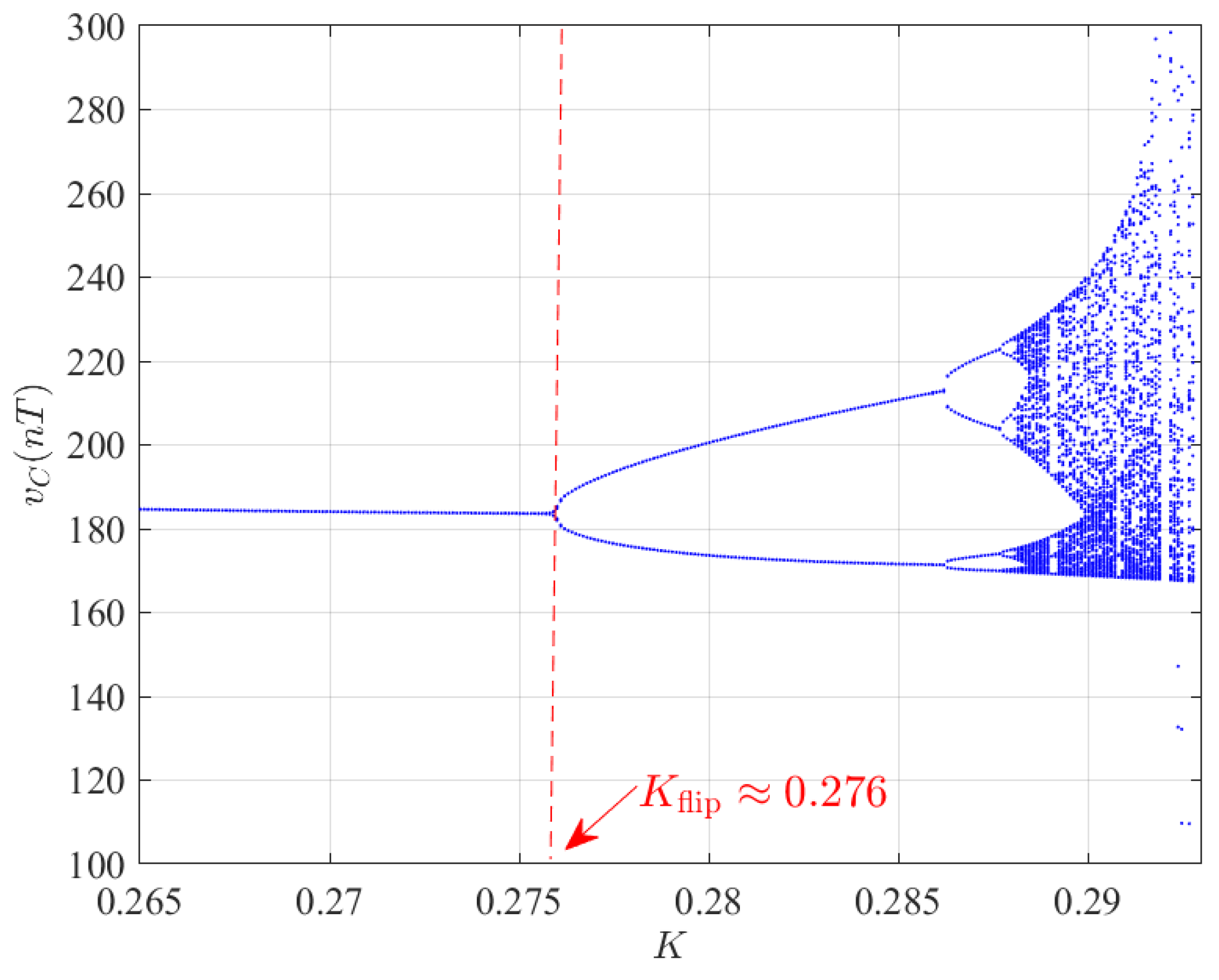
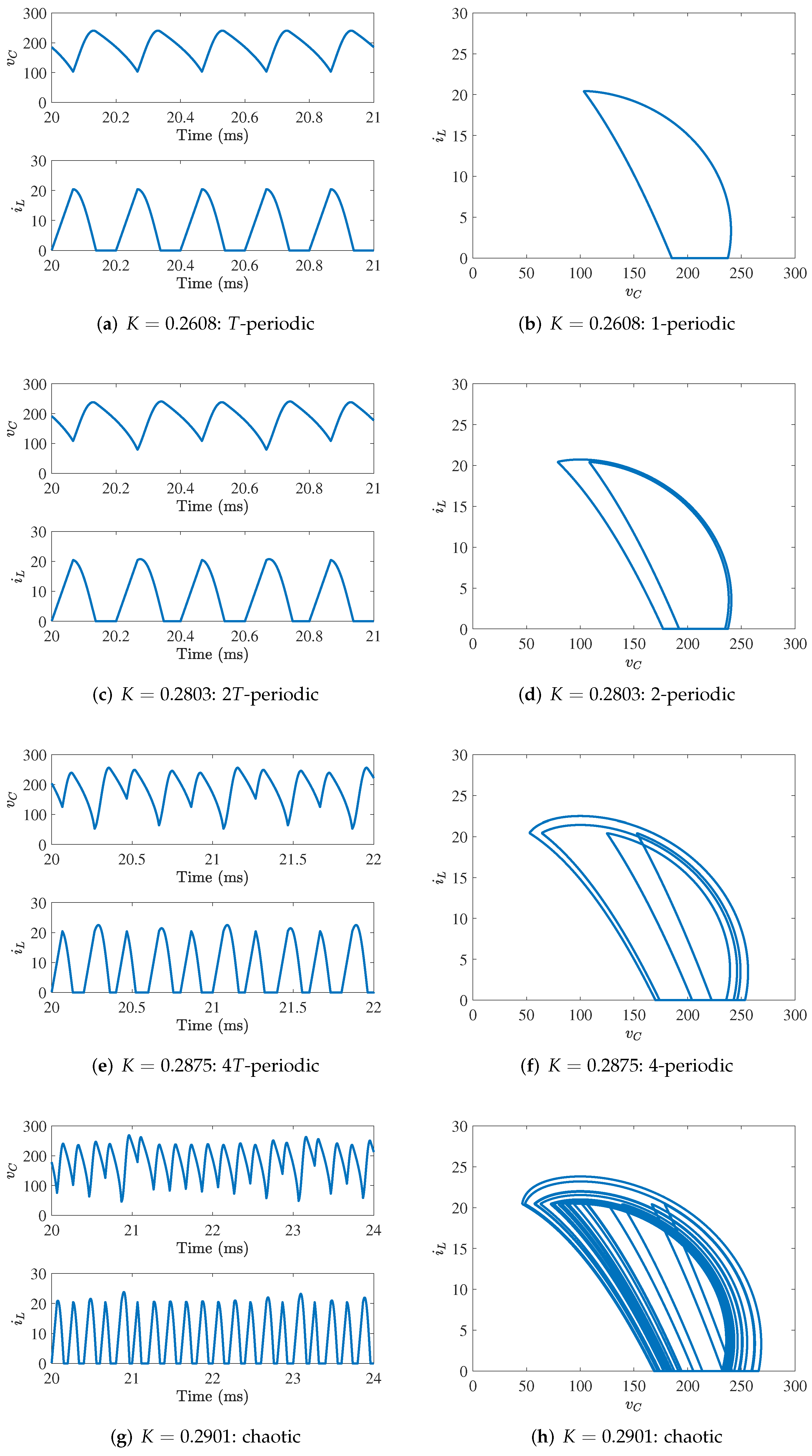
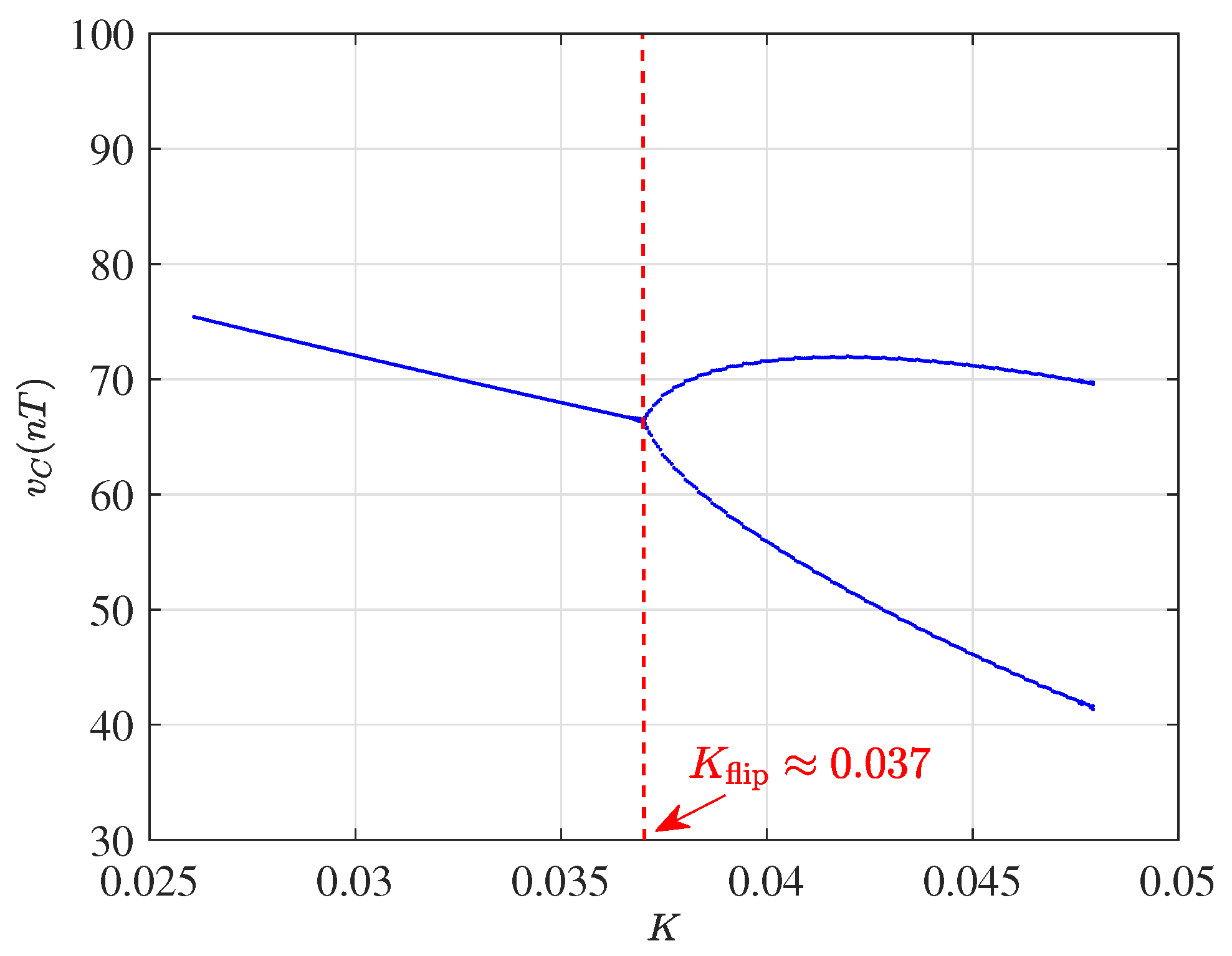
7. Period-Doubling Bifurcation of Periodic Orbits in Open-Loop-DCM-Operated DC–DC Converters Feeding CPLs

The fast scale dynamics in the switching period taking into account ripples in the state variables cannot be predicted by the averaging approach. In this section, the switched model is used for predicting period-doubling bifurcation in the open-loop-DCM-operated boost and the buck converters with CPLs.

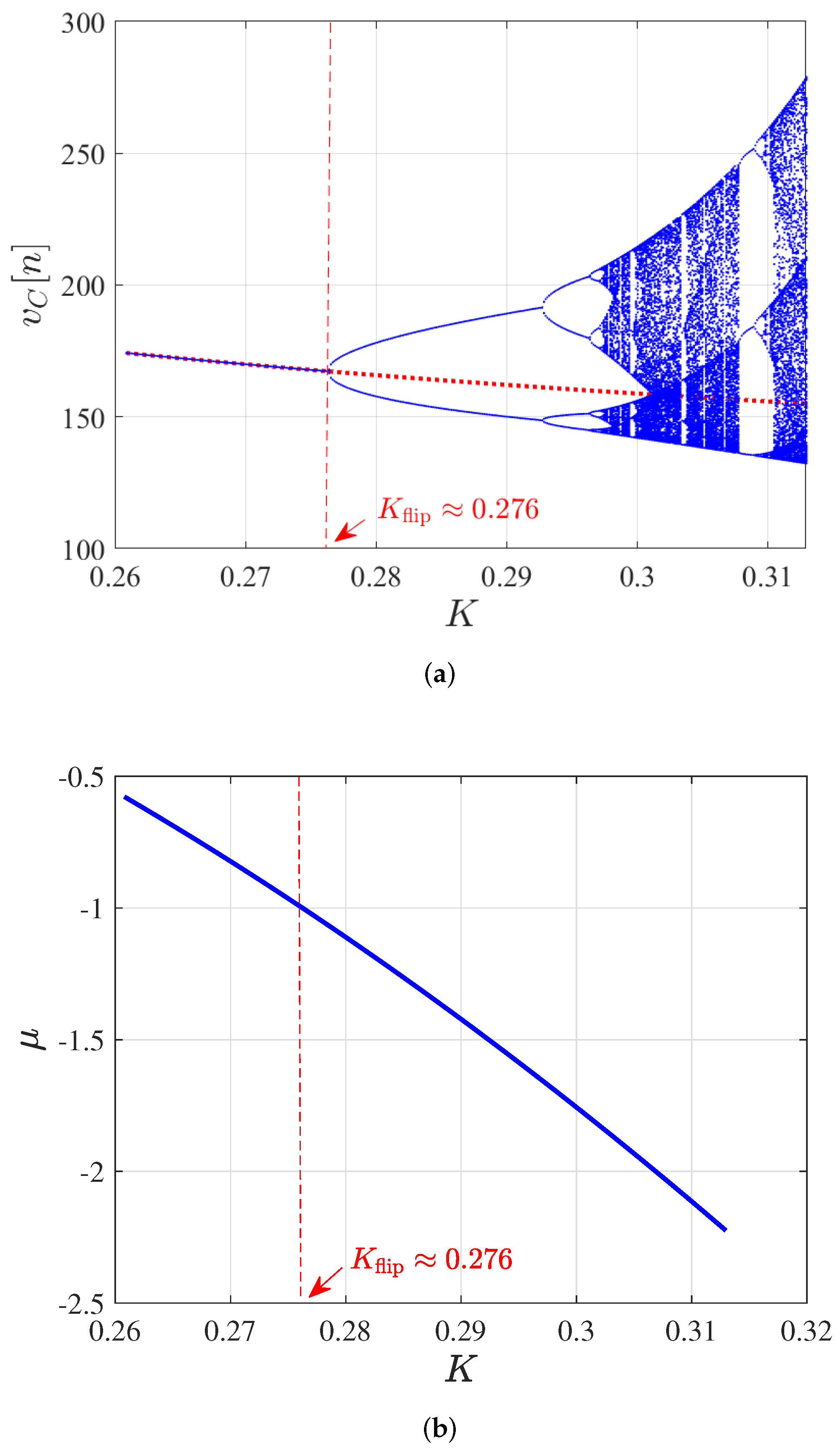
7.1. The Boost Converter

To reveal the possible dynamical behaviors that can exhibit a DCM-operated boost converter with a CPL, a bifurcation diagram was computed using the exact switched model of the converter implemented in the PSIM© software. The result is represented in Figure 10. The used fixed parameter values are depicted in Table 5. The parameter P was taken as a bifurcation parameter, which varied in the range ( 0.80 , 0.96 ) kW. The sampled values of the capacitor voltage v C [ n ] : = v C ( n T ) , n = 0 , 1 , 2 are plotted versus the dimensionless parameter K. Clearly, it can be observed that, from an initial fundamental (one-periodic) orbit, a cascade of period-doubling bifurcations culminates in a chaotic regime. First, a stable two-periodic orbit is generated at a critical value of the power P, P flip 847 W, or equivalently, the dimensionless parameter K, K flip 0.276 , and further variations of the bifurcation parameter P or equivalently K make this emerging orbit also unstable, and so on, finally producing chaotic dynamics. This phenomenon is the celebrated period-doubling bifurcation route to chaos encountered in many mathematical and physical systems. By increasing the bifurcation parameter P a bit further, a non-admissible dynamics, both from a mathematical and a practical point of view due to an unlimited CPL current, comes out. Indeed, the increasing size (interval for v C [ n ] ) of the chaotic attractor due to further variation in the parameter produces the mentioned very high current in the load, and so, the dynamics makes no sense. A numerical integration, for instance with commercial software, would give incoherent results similar to the ones mentioned in Remark 1. The upper value of the bifurcation parameter was selected smaller than the one corresponding to any voltage collapse.
As an important detail, it is worth mentioning that the route to chaos scenario corresponds to the classical period-doubling without border collision bifurcations, widely observed in switching converters [18,19], because the DCM operation is maintained for all the switching cycles even after bifurcations take place. In some cases, not shown here for the simplicity of presentation, it may happen that DCM is not accomplished for all the switching cycles in an arbitrary orbit. Obviously, this fact induces some deviation in the bifurcation diagram regarding the more standard patterns observed in Figure 10, due to discontinuity transitions associated with mixed CCM–DCM operation in a specific orbit.
Representative time domain waveforms and state trajectories are represented in Figure 11. They were obtained using the same fixed parameters as in Figure 10 for different values of the dimensionless parameter K or, equivalently, power P. In this figure, orbits of different periodicity can be observed. The case of Figure 11a,b corresponds to a fundamental DCM one-periodic orbit. Figure 11c,d stand for the subharmonic oscillation with a periodicity of two produced; after that, the fundamental one-orbit loses its stability by a conventional smooth period-doubling bifurcation. The resulting DCM two-periodic orbit evolves such that it undergoes a period-doubling resulting in the DCM four-periodic orbit represented in Figure 11e,f. Finally, Figure 11g,h represent a DCM chaotic attractor.

7.2. The Buck Converter

The region of DCM operation in the parametric space for the buck converter is much smaller than the one corresponding to the boost converter (Figure 7). The set of parameter values of Table 5 was also used here for the buck converter. A bifurcation diagram of the converter was computed using the PSIM© software. The result is shown in Figure 12. It was observed that the system only exhibited a first period-doubling bifurcation at a critical value P flip 113 W of the power P (equivalently, at a critical value K flip 0.037 of K) without the period-doubling cascade route to chaos. After that, the DCM two-periodic orbit emerged, and it existed for values of P lower than another critical value. By increasing P further, the destructive unlimited current phenomenon took place. The upper value of the bifurcation parameter was selected smaller than the value at which this phenomenon occurred ( K < 0.049 ) (equivalently, P < 150 W).

8. Approximate Explicit 1D Discrete-Time Model and Fast-Scale Stability Limits

8.1. Boost Converter

8.1.1. Approximate Map

The discrete-time model of a switching converter is usually obtained by first obtaining the system response in the time domain and sampling it in synchronicity with the switching period. For switching converters with a CPL, an analytical expression for the system response is not available in continuous time for all sub-circuits. Therefore, here, we proceed in a different way. By performing a forward Euler discretization of the averaged model (2), one obtains the following discrete-time model for the open-loop-DCM-operated boost converter loaded by a CPL.
v C [ n + 1 ] = f ( v C [ n ] )
where f ( v C [ n ] ) is given by the following expression:
f ( v C [ n ] ) = v C [ n ] P T C 1 v C [ n ] 1 v C [ n ] V i D 2 K
The model is only valid if the converter is effectively working in DCM, i.e., for K < K cri . Otherwise, CCM will take place, and the model is no longer valid.
A bifurcation diagram obtained from the model in (12) by taking the parameter K as a bifurcation parameter is depicted in Figure 13a, where a cascade of period-doubling bifurcation was obtained and a good agreement can be observed with Figure 10.

8.1.2. Fixed Points and Their Stability

The fixed point of the map f ( · ) can be found by solving the equation f ( v C [ n ] ) v C [ n ] = 0 for v C [ n ] . In doing so, the expression of the fixed point is the same as the one obtained for the equilibrium point of the averaged mode, that is V C in Table 4, for the boost converter. The evolution of fixed point is represented by the dotted line Figure 13a. Its stability status can be estimated by the characteristic multiplier, which is defined by
μ = d d v C [ n ] f ( v C [ n ] ) v C [ n ] = V C
By applying (13) to (12), μ results:
μ = 1 + P T C 1 V C 2 1 ( V C V i ) 2 D 2 K
After some algebra, taking into account the value of V C in Table 4, the characteristic multiplier for the boost can be expressed as
μ = 1 K D 2 3 T 2 2 L C D 2 K
The behavior of the converter around a fixed point generally depends on whether the absolute value of the characteristic multiplier μ is greater or smaller than one. If it is smaller than one, the fixed point is an attractor, and if it is greater than one, it is a repellor. When μ crosses 1 as a parameter is varied, this possibly indicates a period-doubling bifurcation. In Figure 13b, the characteristic multiplier is plotted in terms of the bifurcation parameter. Observe that, at the first period-doubling bifurcation point, one has μ = 1 .
For this kind of map, the second iterate f f = f ( 2 ) can also address a new period-doubling bifurcation if the parameter is further modified, and the same can occur for successive iterations of the map. This explains the period-doubling cascade observed in Figure 10 and Figure 13a. Needless to say, the onset of instability can also be predicted by the pole of the discrete-time transfer function corresponding to the map f ( · ) [51]. Indeed, the characteristic multiplier coincides with the discrete-time pole.

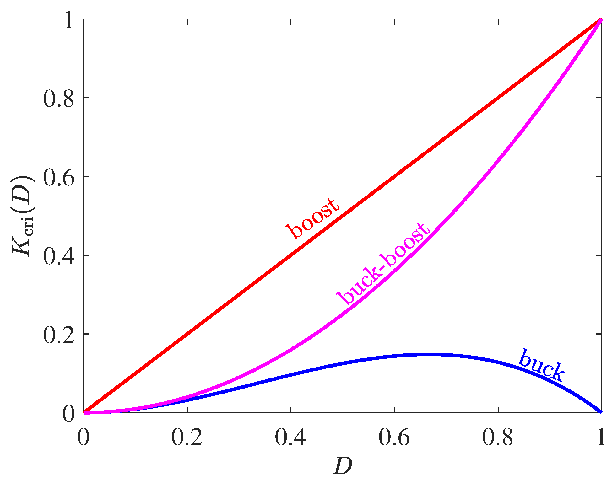
8.1.3. Stability Boundaries in the Parametric Space
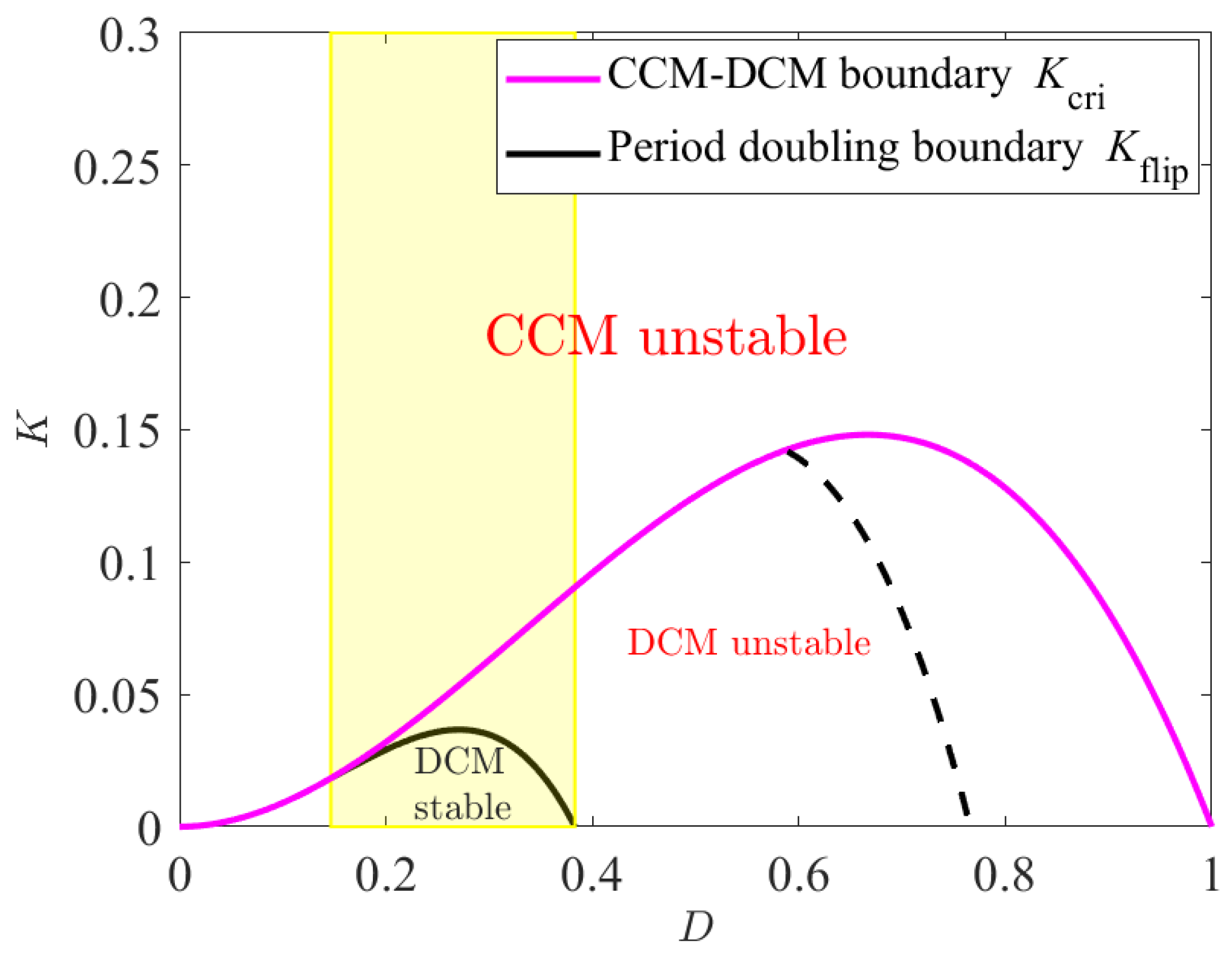
The period-doubling bifurcation boundary can be obtained by making μ = 1 ; hence, from (14), the following condition in terms of the system parameters holds at this boundary:
V i 2 D 2 T 2 2 L C ( V C V i ) 2 2 P T C V C 2 = 0
This is a very useful expression for delimiting the stability boundary in the parameter space at the fast-switching scale of the converter. Furthermore, from the third-degree K-polynomial in (15), the critical maximum value K flip for guaranteeing the stability is
K flip = A 3 T + 4 L C A T + D D
where A is a constant given by the following expression:
A = 6 L C 9 D T + ( 9 D T ) 2 48 L C 3
Accordingly, the corresponding maximum value P flip of power P can be obtained from (17) and the expression of K in terms of P defined previously. For the parameter values considered in this study, the critical value of the dimensionless parameter K at the flip bifurcation point is K flip 0.276 , and from this, the critical value of the power P is P flip 847 W, in remarkable agreement with the bifurcation diagrams represented in Figure 10 and Figure 13a. In terms of the output capacitance, the closed-form expression obtained from (17) with μ = 1 is simpler and can be written as follows:
C flip = 2 L P T D 2 V i 2 3 8 D 2 L 2 P V i 4
Figure 14 shows the regions of the dynamical behavior of the open-loop-DCM-operated boost converter with a CPL in the parametric plane ( D , K ) . The DCM-operated converter is stable below the period-doubling boundary line. Increasing the capacitance C makes the stability region wider. In this case, the period-doubling bifurcation curve is monotonously increasing in terms of the duty cycle D.
Note that a maximum value D flip , max of the duty cycle D exists, above which period-doubling bifurcation cannot take place, since, in this case, K flip > K cri and the converter will operate in CCM. The expression of D flip , max can be obtained in closed-form by solving the equation K flip K cri = 0 . Taking into account that K cri = D (see Table 3 for the boost converter), the following expression for D flip , max from (15), with μ = 1 , is obtained:
D flip , max = 1 4 L C T 2 3
Under the circuit parameters in Table 5, the value D flip , max = 0.473 is obtained. This particular value of the duty cycle D is illustrated in Figure 14 as a vertical dashed line.

8.2. Buck Converter

8.2.1. Approximate Map

Following the same procedures as the ones followed for the boost converter, the map of the open-loop-DCM-operated buck converter is given by the following expression:
f v C [ n ] = v C [ n ] P T C K K D 2 v C [ n ] + D 2 V i

8.2.2. Fixed Point and Its Stability

The expression of the fixed point is the same as in Table 3. Its stability can be determined by the characteristic multiplier, which can be expressed for the DCM-operated open-loop buck converter with a CPL as follows:
μ = 1 T D 2 2 2 L C ( D 2 K )
The critical value of K at the border of instability ( μ = 1 ) is given by
K flip = D 2 1 T 2 D 2 4 L C
With the parameter values of Table 5, the critical value K flip of K at which period-doubling bifurcation takes place is K flip 0.027 , corresponding to a critical value P flip 83 W of the power P. It is worth noting that this approximation of the critical bifurcation parameter value is smaller than the one obtained by the numerical simulations shown in Figure 12 from the exact switched model. The discrepancy is attributed to the Euler approximation used to obtain the explicit discrete-time model from the averaged continuous-time model. Such an approximation is more accurate for the boost converter for which the capacitor voltage is piecewise linear than for the buck topology for which the capacitor voltage is piecewise quadratic. In terms of the output capacitance, the closed-form expression at the bifurcation boundary can be expressed as
C flip = D 4 T 2 4 L ( D 2 K )

8.2.3. Boundaries in the Parameter Space

The expression (23) is only valid if 0 < K flip < K cri for legitimately representing the period-doubling bifurcation boundary. This takes place for values of the duty cycle D within a certain interval ( D flip , min , D flip , max ) . Solving the equations K flip K cri = 0 and K flip = 0 for the duty cycle D, the following expressions for D flip , min and D flip , max are obtained:
D flip , min = 4 L C T 2 , D flip , max = D flip , min
Figure 15 shows the regions of the dynamical behavior of the open-loop-DCM-operated buck converter with a CPL in the plane ( D , K ) . If D flip , min < D < D flip , max , period-doubling bifurcation is expected to take place for K flip < K < K cri . The interval ( D flip , min , D flip , max ) is shown as a yellow strip in Figure 15.
For K cri < K flip < K , it may happen that period-doubling bifurcation coexists with low-frequency oscillation [52], since, in this case, the converter will operate in CCM and an open-loop converter with a CPL operating in this mode is unstable at the slow scale. This will give rise to a mixed mode of operation in which, during some cycles, DCM will take place in the subharmonic regime, and during other cycles, CCM will occur, showing instability at the slow scale. If D flip , min < 2 L C / T , the expression of K flip as a function of D presents a maximum K flip , max at D = 2 L C / T . If D flip , min > 2 L C / T , the maximum value K flip , max is larger than K cri and K flip will be monotonously decreasing within the legitimate range of duty cycle D. This occurs if the capacitance C or inductance L are increased or the period T is decreased. The interval ( D flip , min , D flip , max ) moves to the right in this case. Figure 15 shows in the dashed line an example of such a monotonously decreasing K flip curve for a relatively larger value of the capacitance ( C = 18 μF) than that shown in Table 5.
Note that, because D < 1 , the expression of D flip , max is legitimate only if 2 L C < T . In the opposite case, the interval of D within which period-doubling bifurcation may take place disappears. Therefore, a possible way to make the open-loop-DCM-operated converter be free from period-doubling bifurcation is to make D flip , max illegitimate, hence making T < 2 L C .
Finally, it is worth noting that a further accurate analysis based on an implicit discrete-time modeling [53], not shown here for simplicity, revealed that, while the approximate expressions for predicting period-doubling bifurcation boundary were quite accurate in the case of the boost converter, the ones corresponding to the buck converter presented a significant error. For instance, the exact value of D flip , max corresponding to the buck converter was larger than the one predicted by (25), and consequently, the exact theoretical width of the interval ( D flip , min , D flip , max ) was larger than the approximated one. Therefore, the analytical results presented in this section for the buck converter are only indicative.

9. Conclusions

In this work, we focused on studying the dynamics of open-loop DC–DC converters with CPLs operating in DCM. First, it was shown that a DCM-operated boost converter loaded by a tightly regulated voltage-mode-controlled buck converter may exhibit period-doubling bifurcation for certain values of the system parameters. The performed experimental measurements from a DCM-operated boost converter with a CPL showed that the system may exhibit practically the same behavior. Therefore, the work focused on the dynamics of the three elementary converters loaded by an ideal CPL. Numerical simulations from the switched model revealed that, for the boost converter, after the fundamental one-periodic orbit loses stability, a standard scenario of successive period-doubling leads to a chaotic attractor. Further variation of the bifurcation parameter may lead the system to exhibit destructive dynamics associated with low output voltage and, consequently, unlimited output load current. In the case of the buck converter, only the first period-doubling bifurcation was observed, and the destructive behavior due to unlimited output current interrupted the period-doubling cascade. Approximate discrete-time models were derived for the three elementary converters. The model of the boost converter was demonstrated to accurately predict the onset of the first period-doubling bifurcation for this converter. Concerning the approximate discrete-time model of the buck converter, the analytical results obtained from it were only indicative, and a more accurate numerical analysis is needed for predicting this bifurcation. It was also found that a fundamental periodic orbit does not exist in the case of the buck–boost converter. It is worth noting that, in the previous study, ideal circuit elements were considered. However, in a real circuit, parasitic elements such as the DC resistance of the inductor, the equivalent series resistance of the capacitor, the ON resistance and the OFF resistance of the transistor, and the forward-voltage diode could have an effect on the dynamic behavior of the converter. Namely, they can slightly modify the critical values of other more relevant circuit parameter values at the onset of period-doubling bifurcation and other complex behavior. However, the approximate discrete-time models with ideal circuit elements, despite their simplicity, were shown to display the most-important and -essential features of the corresponding switching converters.

Author Contributions

Conceptualization, L.B. and A.E.A.; methodology, L.B., L.M.-S. and A.E.A.; software, L.B. and A.E.A.; experimental validation, R.H.; formal analysis, A.E.A. and L.B.; investigation, L.B. and A.E.A.; resources, A.E.A. and L.M.-S.; data C.K.T. and L.M.-S.; writing—original draft preparation, A.E.A.; writing—review and editing, L.M.-S. and C.K.T.; visualization, C.K.T.; supervision, A.E.A. and L.M.-S.; project administration, A.E.A.; funding acquisition, A.E.A. All authors have read and agreed to the published version of the manuscript.

Funding

This work was sponsored by the Spanish Ministerio de Ciencia e Innovación under Grants PID2020-120151RB-I00 and PID2019-111443RB-I00. C.K. Tse acknowledges the support of the Honk-Kong Research Grant Council under Grant GRF 11207121.

Data Availability Statement

Te data used to support the fundings of this study are available from the corresponding author upon request.

Conflicts of Interest

The authors declare no conflict of interest.

References

  1. Emadi, A.; Ehsani, A. Dynamics and control of multi-converter DC power electronic systems. In Proceedings of the 2001 IEEE 32nd Annual Power Electronics Specialists Conference, Vancouver, BC, Canada, 17–21 June 2001; Volume 1, pp. 248–253. [Google Scholar]
  2. Khaligh, A. Realization of parasitics in stability of DC–DC converters loaded by constant power loads in advanced multiconverter automotive systems. IEEE Trans. Ind. Electron. 2008, 55, 2295–2305. [Google Scholar] [CrossRef]
  3. Rivetta, C.; Emadi, A.; Williamson, G.A.; Jayabalan, R.; Fahimi, B. Analysis and control of a buck DC–DC converter operating with constant power load in sea and undersea vehicles. IEEE Trans. Ind. Appl. 2004, 2, 1146–1153. [Google Scholar]
  4. Sulligoi, G.; Bosich, D.; Giadrossi, G.; Zhu, L.; Cupelli, M.; Monti, A. Multiconverter medium voltage DC power systems on ships, constant power loads instability solution using linearization via state feedback control. IEEE Trans. Smart Grids 2014, 5, 2543–2552. [Google Scholar] [CrossRef]
  5. Rahimi, A.M.; Emadi, A. An analytical investigation of DC/DC power electronic converters with Constant power loads in vehicular power systems. IEEE Trans. Veh. Technol. 2009, 58, 2689–2702. [Google Scholar] [CrossRef]
  6. Kwasinski, A.; Onwuchekwa, C.N. Dynamic behavior and stabilization of DC microgrids with instantaneous constant-power loads. IEEE Trans. Power Electron. 2011, 26, 822–834. [Google Scholar] [CrossRef]
  7. Lu, X.; Sun, K.; Guerrero, J.M.; Vasquez, J.C.; Huang, L.; Wang, J. Stability enhancement based on virtual impedance for DC microgrids with constant power loads. IEEE Trans. Smart Grid 2015, 6, 2770–2783. [Google Scholar] [CrossRef] [Green Version]
  8. Wu, M.; Lu, D.D.-C. A novel stabilization method of LC input filter with constant power loads without load performance compromise in DC microgrids. IEEE Trans. Ind. Electron. 2015, 62, 4552–4562. [Google Scholar] [CrossRef]
  9. Al-Nussairi, M.K.; Bayindir, R.; Padmanaban, S.; Popa, L.M.; Siano, P. Constant power loads (CPL) with microgrids: Problem definition, stability analysis and compensation techniques. Energies 2017, 10, 1656. [Google Scholar] [CrossRef]
  10. Griffo, A.; Wang, J. Large signal stability analysis of ‘more electric’ aircraft power systems with constant power loads. IEEE Trans. Aerosp. Electron. Syst. 2012, 48, 477–489. [Google Scholar] [CrossRef]
  11. Belkhayat, M.; Cooley, R.; Witulski, A. Large signal stability criteria for distributed systems with constant power loads. In Proceedings of the 26th Annual IEEE Power Electronics Specialists Conference, PESC’95 Record, Atlanta, GA, USA, 18–22 June 1995; Volume 2, pp. 1333–1338. [Google Scholar]
  12. Li, Y.; Vannorsdel, K.R.; Zirger, A.J.; Norris, M.; Maksimović, D. Current mode control for boost converters with constant power loads. IEEE Trans. Circuits Syst. I Fundam. Theory Appl. 2012, 59, 198–206. [Google Scholar] [CrossRef]
  13. Choi, B.; Cho, B.H.; Hong, S.-S. Dynamics and control of DC-to-DC converters driving other converters downstream. IEEE Trans. Circuits Syst. I Fundam. Appl. 1999, 46, 1240–1248. [Google Scholar] [CrossRef]
  14. Emadi, A.; Khaligh, A.; Rivetta, C.H.; Williamson, G.A. Constant power loads and negative impedance instability in automotive systems: Definition, modeling, stability, and control of power electronic converters and motor drives. IEEE Trans. Vehecular Technol. 2006, 55, 1112–1125. [Google Scholar] [CrossRef]
  15. Tse, C.K.; Adams, K.M. Qualitative analysis and control of a DC-to-DC boost converter operating in discontinuous mode. IEEE Trans. Power Electron. 1990, 5, 323–330. [Google Scholar] [CrossRef]
  16. Middlebrook, R.D. Input filter considerations in design and applications of switching regulators. In Proceedings of the IEEE Industry Applications Society Annual Meeting, Chicago, IL, USA, 11–14 October 1976; pp. 91–107. [Google Scholar]
  17. Deane, J.H.B.; Hamill, D.C. Instability, subharmonics, and chaos in power electronic systems. IEEE Trans. Power Electron. 1990, 5, 260–268. [Google Scholar] [CrossRef]
  18. Banerjee, S.; Verghese, G.C. Nonlinear Phenomena in Power Electronics—Attractors, Bifurcations, Chaos, and Nonlinear Control; IEEE Press: Piscataway, NJ, USA, 2001. [Google Scholar]
  19. Tse, C.K. Complex Behavior of Switching Power Converters; CRC Press: Boca Raton, FL, USA, 2003. [Google Scholar]
  20. Emadi, A.; Fahimi, B.; Ehsani, M. On the concept of negative impedance instability in the more electric aircraft power systems with constant power loads. SAE Trans. 1999, 108, 689–699. [Google Scholar]
  21. Smithson, S.C.; Williamson, S.S. Constant power loads in more electric vehicles—An overview. In Proceedings of the IECON 2012—38th Annual Conference on IEEE Industrial Electronics Society, Montreal, QC, Canada, 25–28 October 2012; pp. 2914–2922. [Google Scholar]
  22. Grigore, V.; Hatonen, J.; Kyyra, J.; Suntio, T. Dynamics of a buck converter with a constant power load. In Proceedings of the 29th IEEE Power Electronics Specialists Conference, Fukuoka, Japan, 22 May 1998; pp. 72–78. [Google Scholar]
  23. Rahimi, A.; Emadi, A. Discontinuous-conduction mode DC/DC converters feeding constant-power loads. IEEE Trans. Ind. Electron. 2010, 57, 1318–1329. [Google Scholar] [CrossRef]
  24. Hamill, D.C.; Deane, J.H.B.; Jefferies, D. Modeling of chaotic DC–DC converters by iterated nonlinear mappings. IEEE Trans. Power Electron. 1992, 7, 25–36. [Google Scholar] [CrossRef]
  25. Di Bernardo, M.; Vasca, F. Discrete-time maps for the analysis of bifurcations and chaos in DC/DC converters. IEEE Trans. Circuits Syst. I Fundam. Theory Appl. 2000, 47, 130–143. [Google Scholar] [CrossRef]
  26. Chakrabarty, K.; Poddar, G.; Banerjee, S. Bifurcation behavior of the buck converter. IEEE Trans. Power Electron. 1996, 11, 439–447. [Google Scholar] [CrossRef]
  27. Fossas, E.; Olivar, G. Study of chaos in the buck converter. IEEE Trans. Circuits Syst. I Fundam. Theory Appl. 1996, 43, 13–25. [Google Scholar] [CrossRef] [Green Version]
  28. Papafotiou, G.A.; Margaris, N.I. Calculation and stability investigation of periodic steady-states of the voltage controlled Buck DC–DC converter. IEEE Trans. Power Electron. 2004, 19, 959–970. [Google Scholar] [CrossRef]
  29. Chu, G.; Tse, C.K.; Wong, S.C. Line-frequency instability of PFC power supplies. IEEE Trans. Power Electron. 2009, 24, 469–482. [Google Scholar] [CrossRef]
  30. El Aroudi, A.; Haroun, R.; Al-Numay, M.; Calvente, J.; Giral, R. A Large-signal model for a peak current mode controlled boost converter with constant power loads. IEEE J. Emerg. Sel. Top. Power Electron. 2021, 9, 559–568. [Google Scholar] [CrossRef]
  31. El Aroudi, A.; Haroun, R.; Al-Numay, M.; Calvente, J.; Giral, R. Fast-scale stability analysis of a DC–DC boost converter with a constant power load. IEEE J. Emerg. Sel. Top. Power Electron. 2019, 9, 549–558. [Google Scholar] [CrossRef]
  32. Cristiano, R.; Pagano, D.J.; Benadero, L.; Ponce, E. Bifurcation analysis of a DC–DC bidirectional power converter operating with constant power loads. Int. J. Bifurc. Chaos 2016, 26, 1630010. [Google Scholar] [CrossRef] [Green Version]
  33. El Aroudi, A.; Debbat, M.; Giral, R.; Martinez-Salamero, L. Quasiperiodic route to chaos in DC–DC switching regulators. In Proceedings of the ISIE 2001, 2001 IEEE International Symposium on Industrial Electronics Proceedings (Cat. No.01TH8570), Pusan, Republic of Korea, 12–16 June 2001; Volume 3, pp. 2130–2135. [Google Scholar]
  34. Zadeh, M.K.; Gavagsaz-Ghoachani, R.; Martin, J.P.; Nahid-Mobarakeh, B.; Pierfederici, S.; Molinas, M. Discrete-time modeling, stability analysis, and active stabilization of DC distribution systems with multiple constant power loads. IEEE Trans. Ind. Appl. 2016, 52, 4888–4898. [Google Scholar] [CrossRef]
  35. Zadeh, M.K.; Gavagsaz-Ghoachani, R.; Martin, J.; Pierfederici, S.; Nahid-Mobarakeh, B.; Molinas, M. Discrete-Time Tool for Stability Analysis of DC Power Electronics-Based Cascaded Systems. IEEE Trans. Power Electron. 2017, 32, 652–667. [Google Scholar] [CrossRef] [Green Version]
  36. Saublet, L.; Gavagsaz-Ghoachani, R.; Martin, J.; Nahid-Mobarakeh, B.; Pierfederici, S. Asymptotic stability analysis of the limit cycle of a cascaded DC–DC converter using sampled discrete-time modeling. IEEE Trans. Ind. Electron. 2016, 63, 2477–2487. [Google Scholar] [CrossRef]
  37. Saublet, L.; Gavagsaz-Ghoachani, R.; Martin, J.; Nahid-Mobarakeh, B.; Pierfederici, S. Bifurcation analysis and stabilization of DC power systems for electrified transportation systems. IEEE Trans. Transp. Electrif. 2016, 2, 86–95. [Google Scholar] [CrossRef]
  38. Tse, C.K. Flip bifurcation and chaos in three-state boost switching regulators. IEEE Trans. Circuits Syst. I Fundam. Theory Appl. 1994, 41, 16–23. [Google Scholar] [CrossRef]
  39. Tse, C.K. Chaos from a buck switching regulator operating in discontinuous mode. Int. J. Circ. Theor. Appl. 1994, 22, 263–278. [Google Scholar] [CrossRef]
  40. Giaouris, D.; Banerjee, S.; Zahawi, B.; Pickert, V. Stability analysis of the continuous conduction mode buck converter via Filippov’s method. IEEE Trans. Circuits Syst. I 2008, 55, 1084–1096. [Google Scholar] [CrossRef] [Green Version]
  41. Cheng, L.; Ki, W.-H.; Yang, F.; Mok, P.K.T.; Jing, X. Predicting subharmonic oscillation of voltage-mode switching converters using a circuit-oriented geometrical approach. IEEE Trans. Circuits Syst. I Regul. Pap. 2017, 64, 717–730. [Google Scholar] [CrossRef]
  42. Redl, R.; Novak, I. Instabilities in current-mode controlled switching voltage regulators. In Proceedings of the 1981 IEEE Power Electronics Specialists Conference, Boulder, CO, USA, 29 June–3 July 1981; pp. 17–28. [Google Scholar]
  43. Zafrany, I.; Ben-Yaakov, S. A chaos model of subharmonic oscillations in current mode PWM boost converters. In Proceedings of the IEEE Power Electronics Specialists Conference, Atlanta, GA, USA, 18–22 June 1995; pp. 1111–1117. [Google Scholar]
  44. Chan, W.C.Y.; Tse, C.K. Study of bifurcations in current-programmed DC/DC boost converters: From quasiperiodicity to period-doubling. IEEE Trans. Circuits Syst. I Fundam. Theory Appl. 1997, 44, 1129–1142. [Google Scholar] [CrossRef] [Green Version]
  45. Tse, C.K.; Chan, W.C.Y. Chaos from a current programmed Cuk converter. Int. J. Circuit Theory Appl. 1995, 23, 217–225. [Google Scholar] [CrossRef]
  46. Deane, H.B.; Hamill, D.C. Chaotic behavior in current-mode controlled DC/DC converters. Inst. Elect. Eng. Electron. Lett. 1991, 13, 1172–1173. [Google Scholar]
  47. Deane, J.H.B. Chaos in a current-mode controlled boost DC/DC converter. IEEE Trans. Circuits Syst. I 1992, 39, 680–683. [Google Scholar] [CrossRef]
  48. Fang, C. Unified Discrete-Time Modeling of Buck Converter in Discontinuous Mode. IEEE Trans. Power Electron. 2011, 26, 2335–2342. [Google Scholar] [CrossRef]
  49. Benadero, L.; Aroudi, A.E.; Martinez-Salamero, L.; Tse, C.K. Period doubling route to chaos in open-loop boost converters under constant power loading and discontinuous conduction mode conditions. In Proceedings of the IEEE International Symposium on Circuits and Systems, (ISCAS 2020), Seville, Spain, 12–14 October 2020. [Google Scholar]
  50. Erickson, R.W.; Maksimovic, D. Fundamentals of Power Electronics; Kluwer Academic Publishers: Amsterdam, The Netherlands, 2001. [Google Scholar]
  51. El Aroudi, A. A new approach for accurate prediction of subharmonic oscillation in switching regulators—Part I: Mathematical derivations. IEEE Trans. Power Electron. 2017, 32, 5651. [Google Scholar] [CrossRef]
  52. Chen, Y.; Tse, C.K.; Qiu, S.S.; Lindenmuller, L.; Schwarz, W. Coexisting fast-scale and slow-scale instability in current-mode controlled DC/DC converters: Analysis, simulation and experimental results. IEEE Trans. Circuits Syst. I Regul. Pap. 2008, 55, 3335–3348. [Google Scholar] [CrossRef] [Green Version]
  53. Benadero, L.; El Aroudi, A.; Martinez-Salamero, L.; Tse, C.K. In-depth analysis of smooth and nonsmooth bifurcations for an open-loop boost converter feeding constant power loads in discontinuous conduction mode. Int. J. Bifurc. Chaos 2022. submitted. [Google Scholar]
Figure 1. An open-loop boost converter loaded by a voltage-mode-controlled buck converter.
Electronics 12 01030 g001
Figure 2. Behavior of an open−loop boost converter operating in DCM loaded by a tightly regulated buck converter and by an ideal CPL. (a,b) P = 800 W: stable periodic regime, (c,d) P = 900 W: subharmonic oscillation.
Electronics 12 01030 g002
Figure 3. The experimental setup to observe period-doubling bifurcation in an open-loop boost converter with a CPL. ➀ Power supply, ➁ Function generator. ➂ Electronic load. ➃ Power supply. ➄ Boost converter circuit. ➅ Oscilloscope.
Electronics 12 01030 g003
Figure 4. Waveforms of an open-loop boost converter operating in DCM loaded by an ideal CPL. (a,b) P = 28 W: stable periodic regime, (c,d) P = 30 W: subharmonic oscillation due to period-doubling bifurcation.
Electronics 12 01030 g004
Figure 5. Elementary switching converters loaded by a CPL: (a) buck, (b) boost, and (c) buck–boost.
Electronics 12 01030 g005
Figure 6. Steady-state inductor current i L at the boundary of CCM–DCM for any elementary converter.
Electronics 12 01030 g006
Figure 7. The critical value K cri of K at the boundary CCM–DCM for elementary switching converters loaded by a CPL. For a specific value of D, if K > K cri ( D ) , CCM takes place, and if K < K cri ( D ) , DCM occurs.
Electronics 12 01030 g007
Figure 8. Sketch of the inductor current i L waveform for any DCM-operated elementary converter.
Electronics 12 01030 g008
Figure 9. The conversion gain M ( D , K ) for the buck and the boost converter for different values of dimensionless parameter K. The conversion gain for CCM is also shown for comparison.
Electronics 12 01030 g009
Figure 10. Bifurcation diagram of the DCM-operated boost converter with a CPL obtained using the PSIM© software.
Electronics 12 01030 g010
Figure 11. Time domain waveforms of the capacitor voltage and the inductor current for different dynamical behaviors obtained from the switched model of an open-loop-DCM-operated boost converter implemented in the PSIM© software.
Electronics 12 01030 g011
Figure 12. Bifurcation diagram of the DCM-operated buck converter with a CPL obtained using the PSIM© software.
Electronics 12 01030 g012
Figure 13. (a) Bifurcation diagram of the open-loop-DCM-operated boost converter with a CPL obtained using the approximated discrete-time model. The evolution of the fixed point is also represented by the dotted line. (b) Characteristic multiplier μ .
Electronics 12 01030 g013
Figure 14. Regions of the dynamical behaviors of the open-loop-DCM-operated boost converter with a CPL in the plane ( D , K ) and the parameter values shown in Table 1.
Electronics 12 01030 g014
Figure 15. Regions of the dynamical behavior of the open-loop-DCM-operated buck converter with a CPL in the plane ( D , K ) .
Electronics 12 01030 g015
Table 1. Parameters used in the numerical simulations of the cascaded boost and buck converters.
Source Converter (Boost)Load Converter (Buck)
Input voltage, V i = 100  VOutput voltage v ref 48 V
Duty cycle, D = 1 3 Load resistance R L variable
Inductance, L 1 = 326 μHInductance L 2 = 250 μH
Capacitance, C 1 = 4.5 μFCapacitance C 2 = 47 μF
Switching frequency f s 1 = 5  kHzSwitching frequency f s 2 = 200  kHz
Table 2. State equations for the three elementary converters with a CPL.
BuckBoostBuck–Boost
d v C d t P C v C + i L C P C v C + ( 1 u ) i L C P C v C + ( 1 u ) i L C
d i L d t v C L + u V i L ( u 1 ) v C L + V i L ( u 1 ) v C L + u V i L
Table 3. Expressions for the steady-state value of the average inductor current I L , the critical value P cri of the power P, and the critical value K cri of the dimensionless parameter K at the boundary of CCM–DCM for the three elementary DC–DC converters operating in DCM.
BuckBoostBuck–Boost
I L P D V i P V i P ( 1 D ) V i
P cri V i 2 D 2 T 2 L 1 D V i 2 D T 2 L V i 2 D 2 T 2 L
K cri D 2 ( 1 D ) D D 2
Table 4. Peak current I P , ratio D , averaged voltage V C , and conversion ratio M ( D , K ) for the three converters with a CPL under DCM operation.
BuckBoostBuck–Boost
I P ( V i V C ) D T L V i D T L V i D T L
D ( V i V C ) D V C V i D V C V i V i D V C
V C V i ( D 2 K ) D 2 V i K K D 2 ¬
M ( D , K ) D 2 K D 2 K K D 2 ¬
Table 5. The used parameter values for the open-loop buck and boost converters loaded by a CPL.
V i LCTD
100 V326 μH4.5 μF200 μs 1 3
Disclaimer/Publisher’s Note: The statements, opinions and data contained in all publications are solely those of the individual author(s) and contributor(s) and not of MDPI and/or the editor(s). MDPI and/or the editor(s) disclaim responsibility for any injury to people or property resulting from any ideas, methods, instructions or products referred to in the content.

