


Complex Dynamics in Digital Nonlinear Oscillators: Experimental Analysis and Verification


Abstract
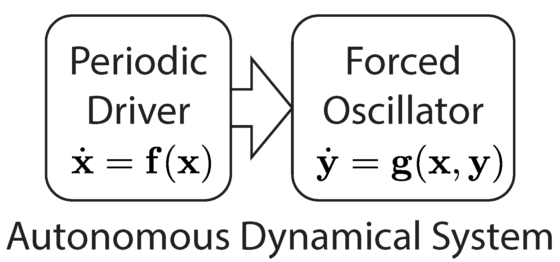
:1. Introduction
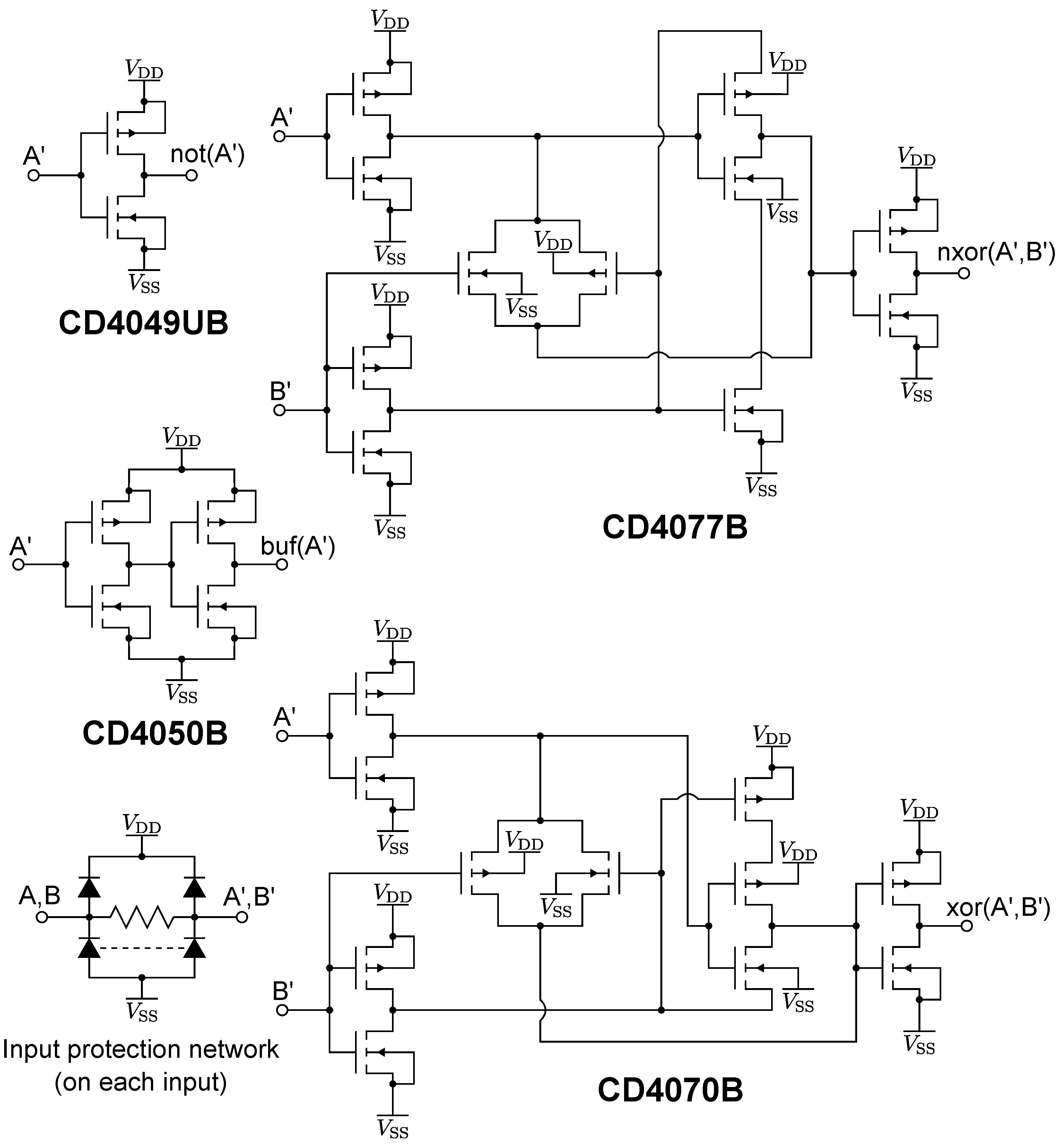
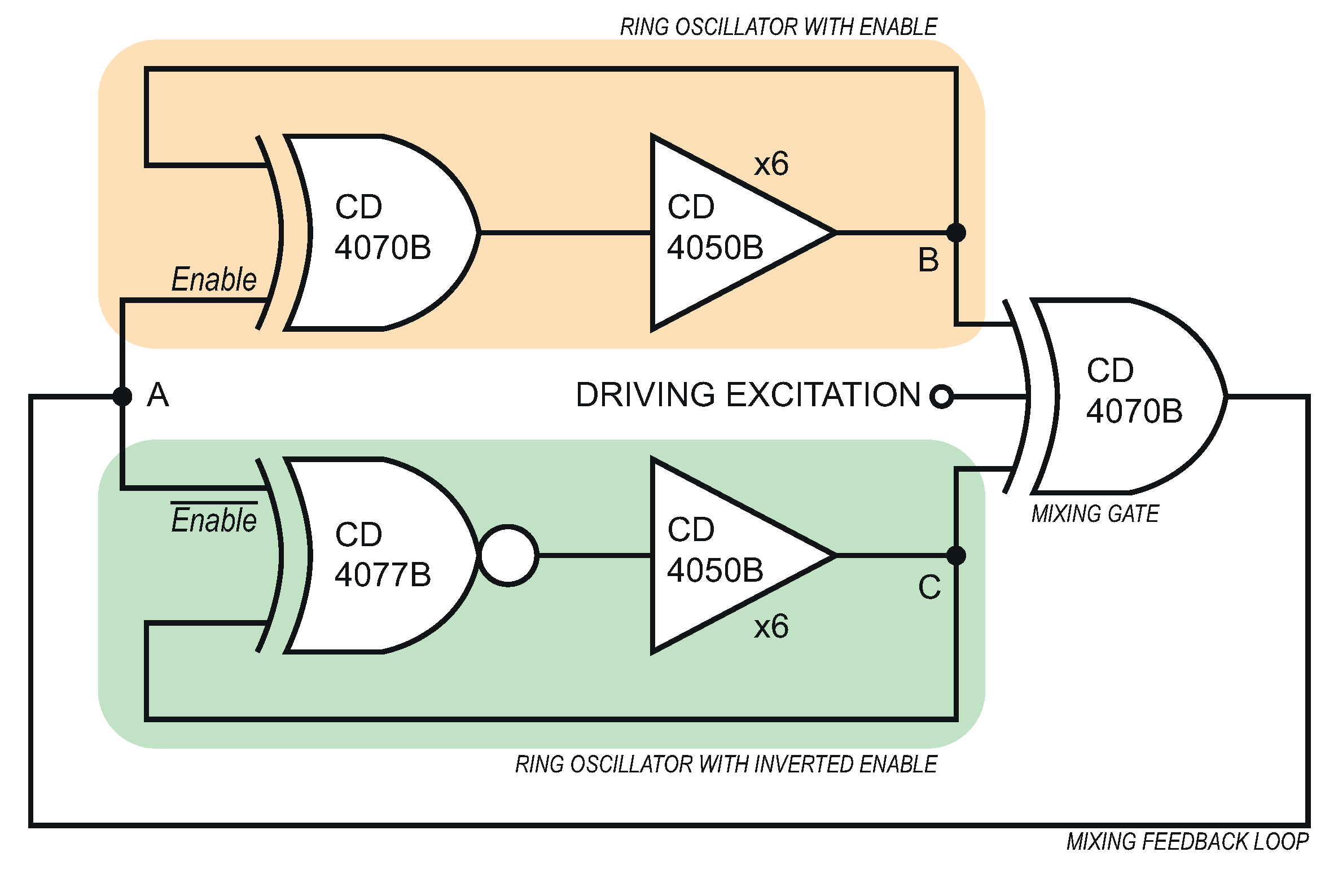
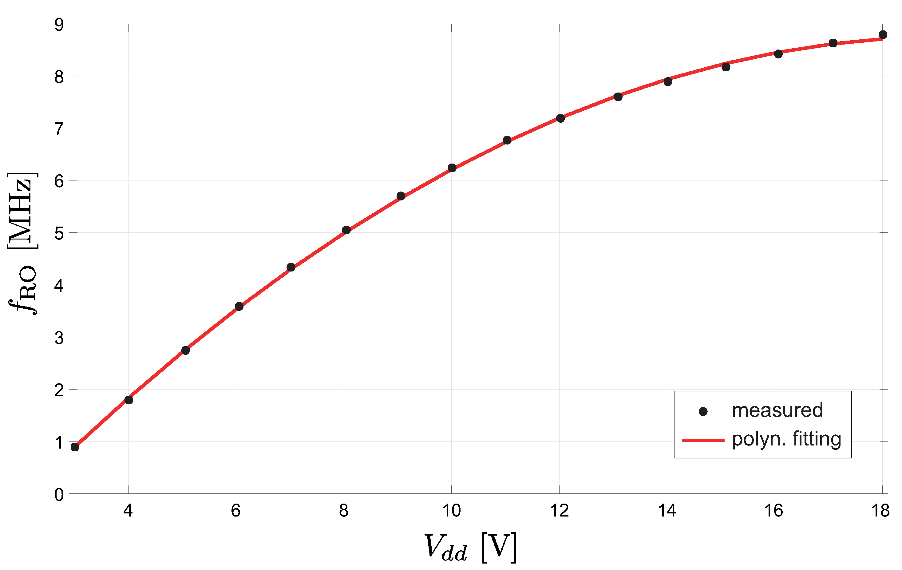
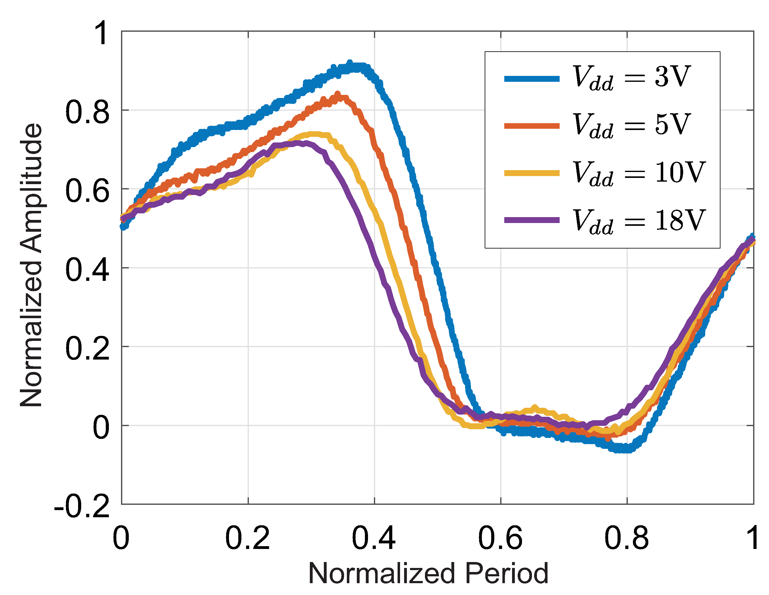
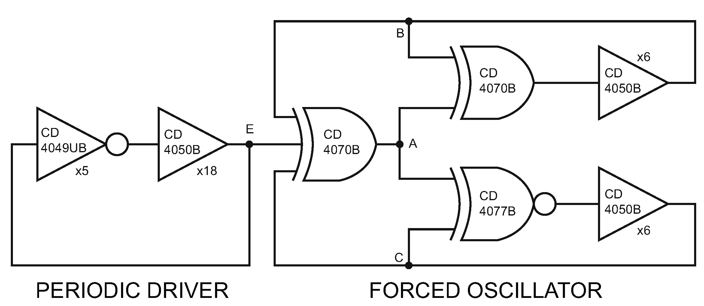
2. Case Study DNO: Design and Implementation
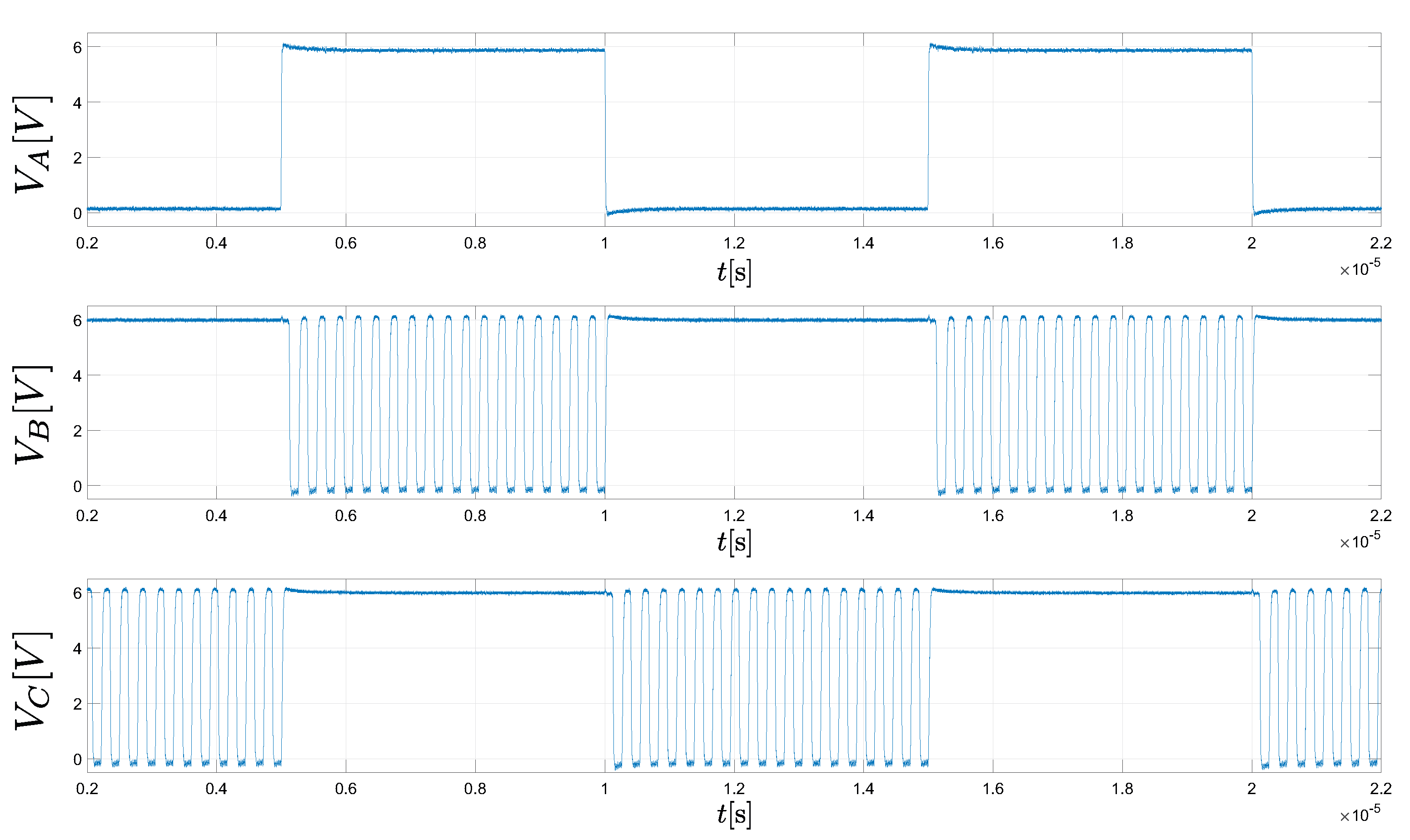
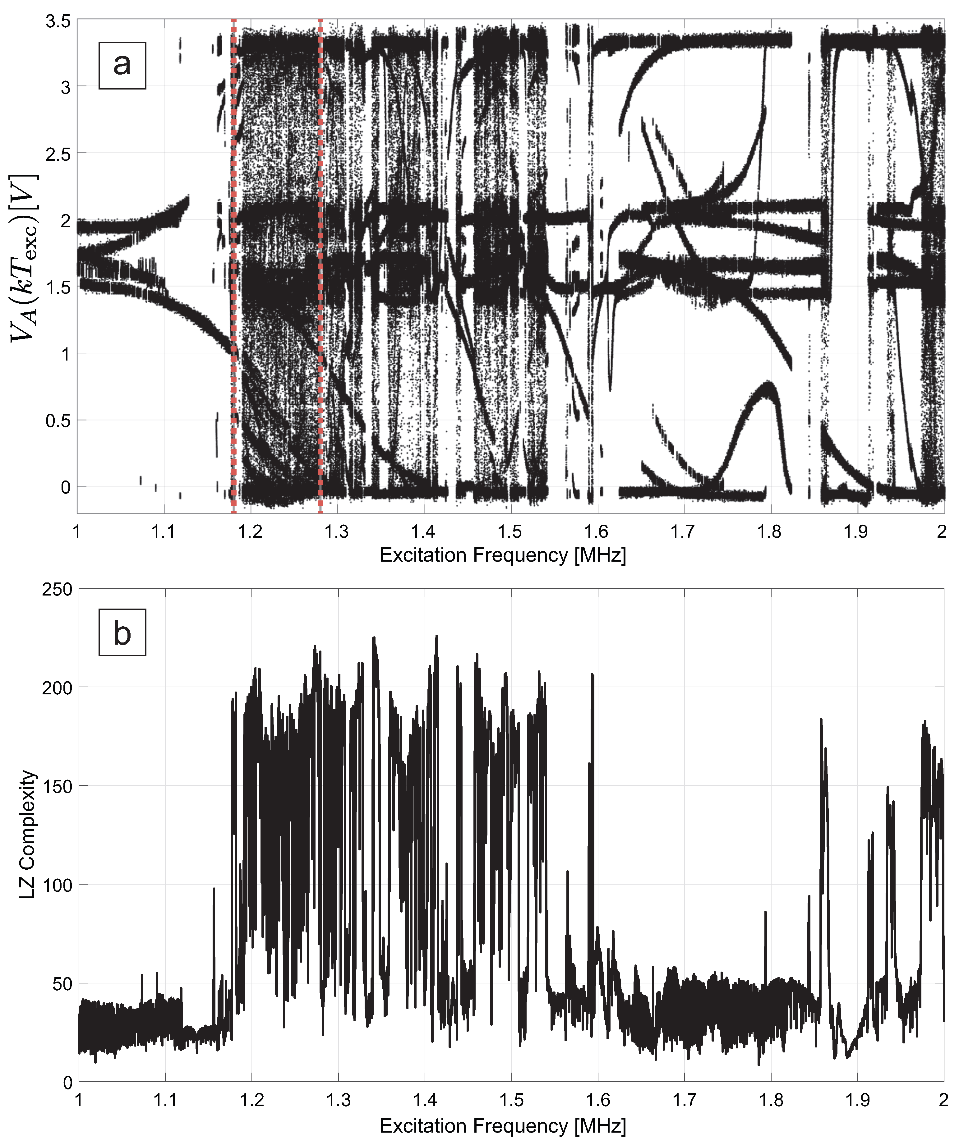
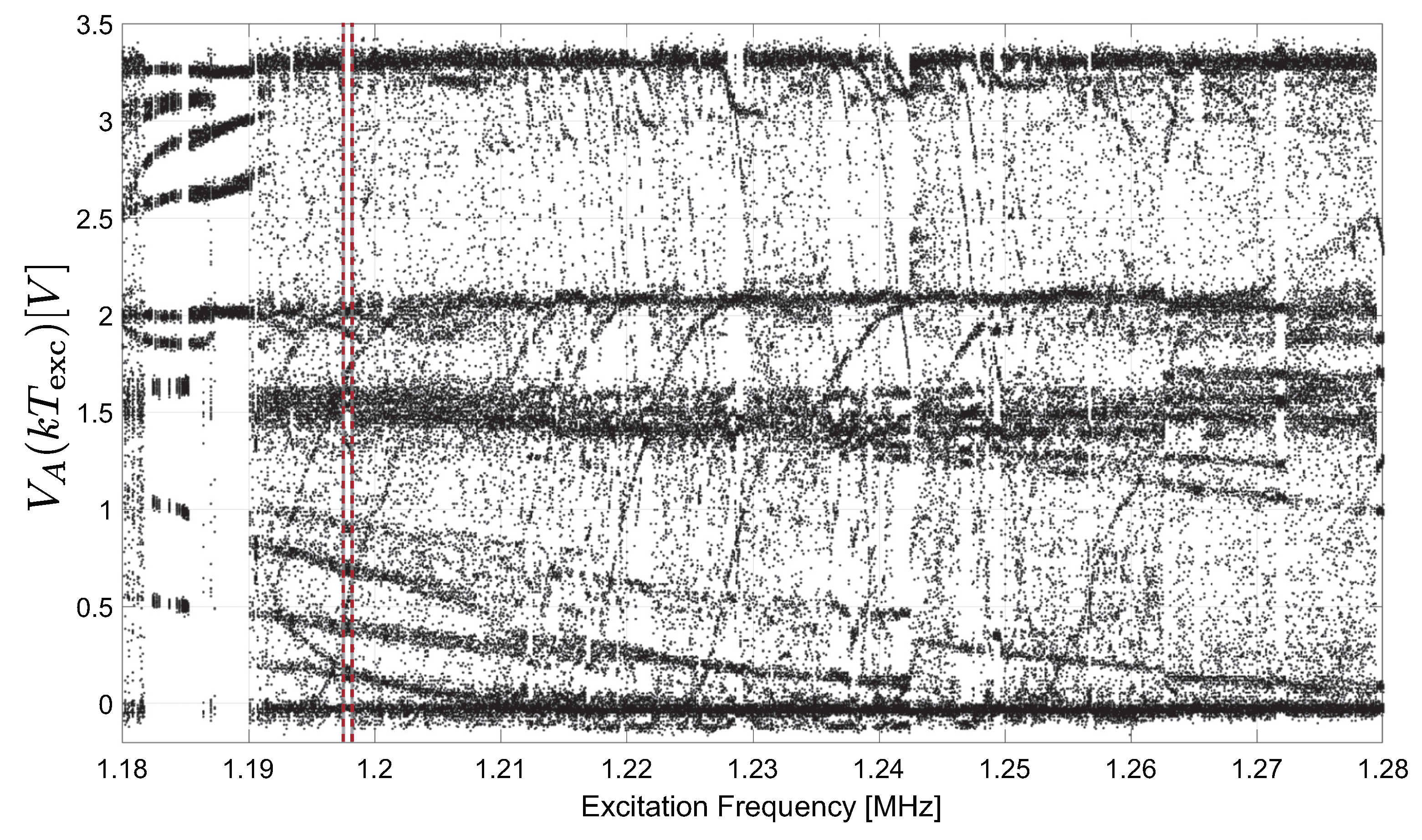
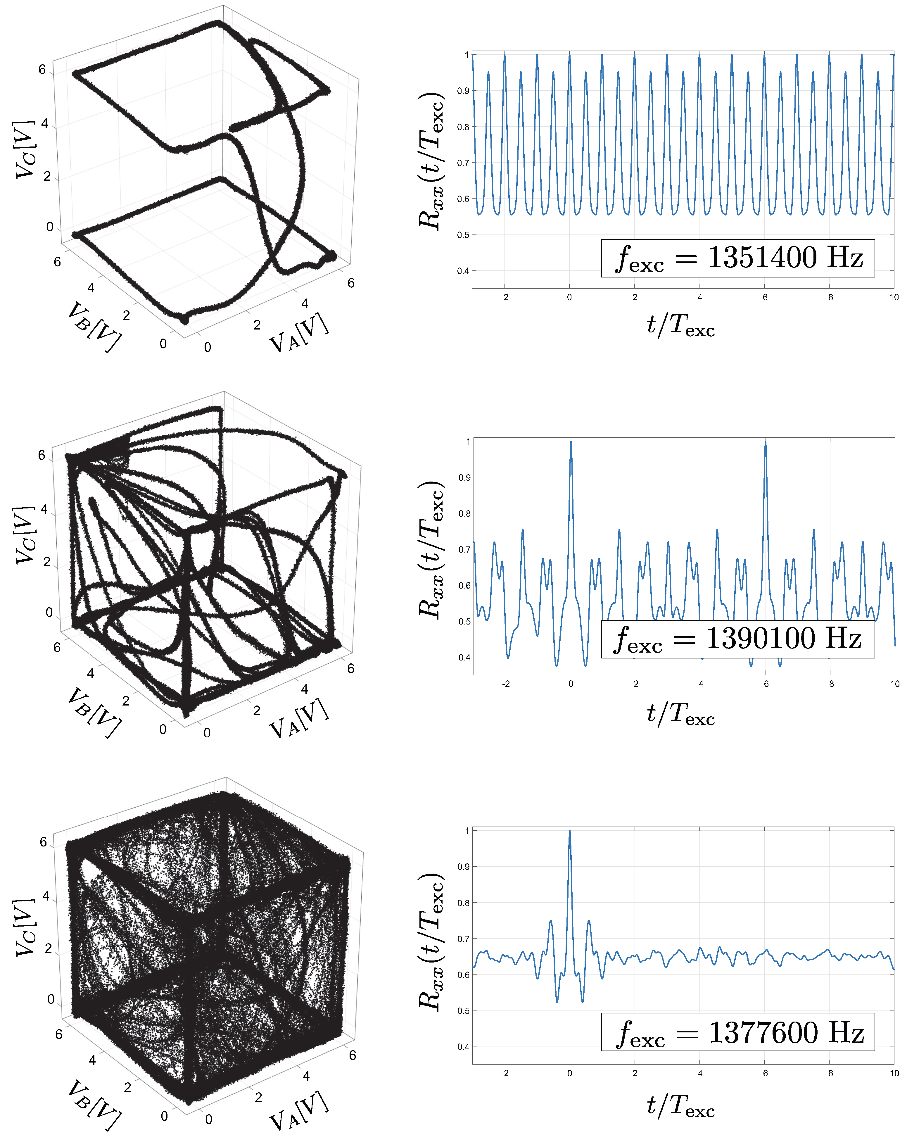
3. Forced Oscillator: Implementation and Analysis
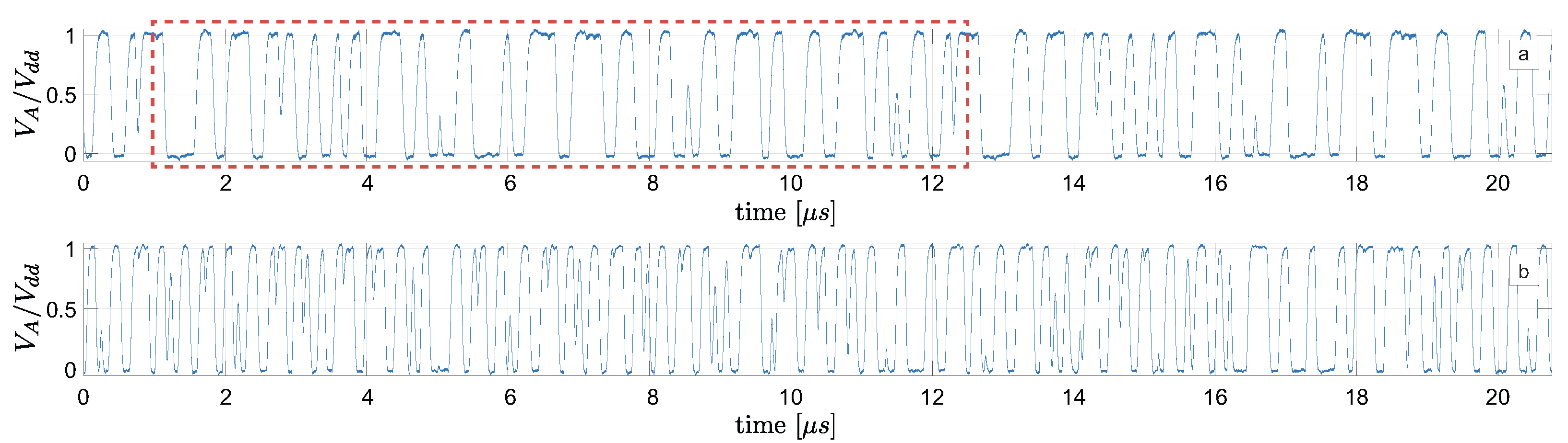
Turned-Off Excitation: Dynamical Behavior
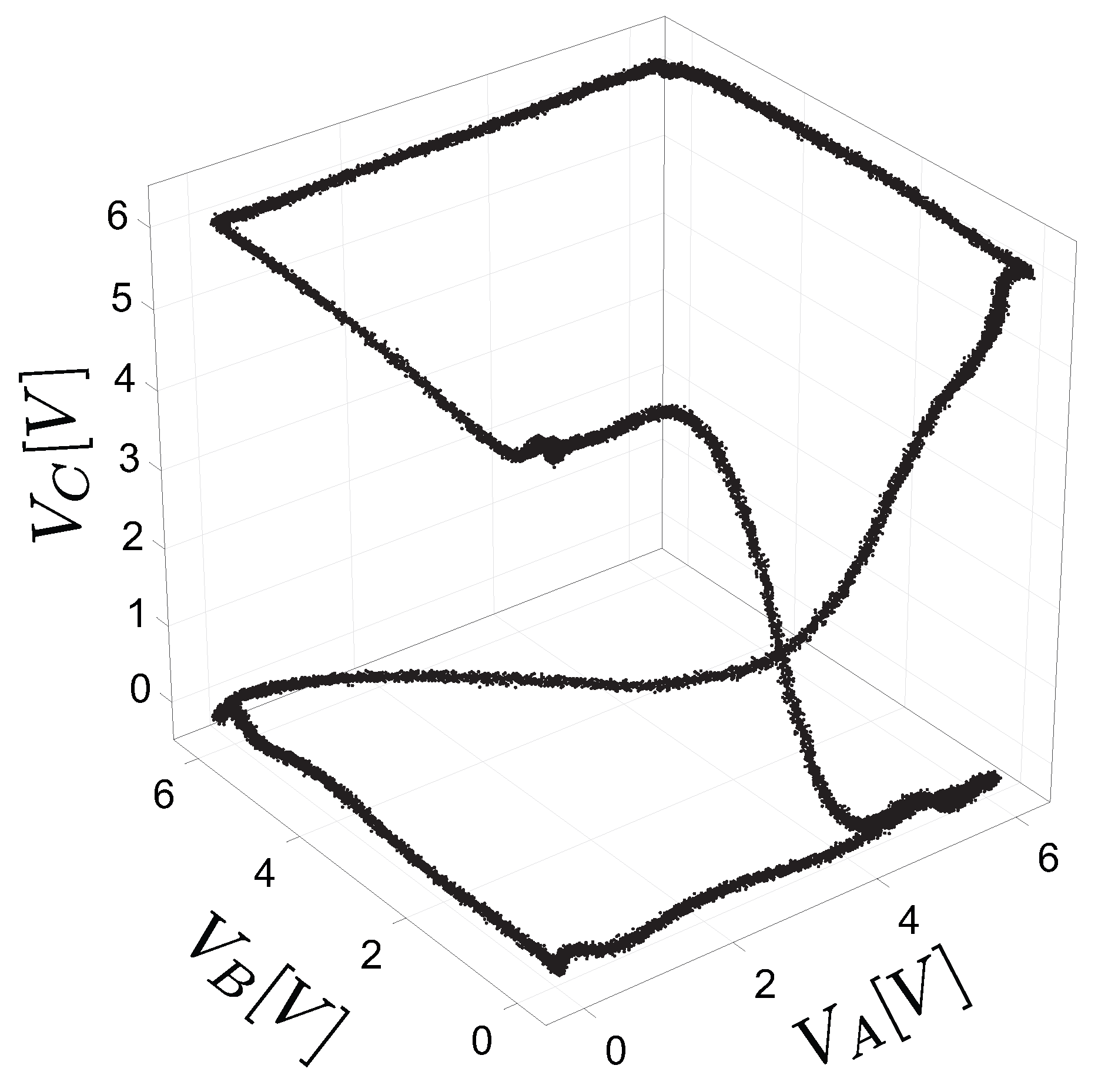
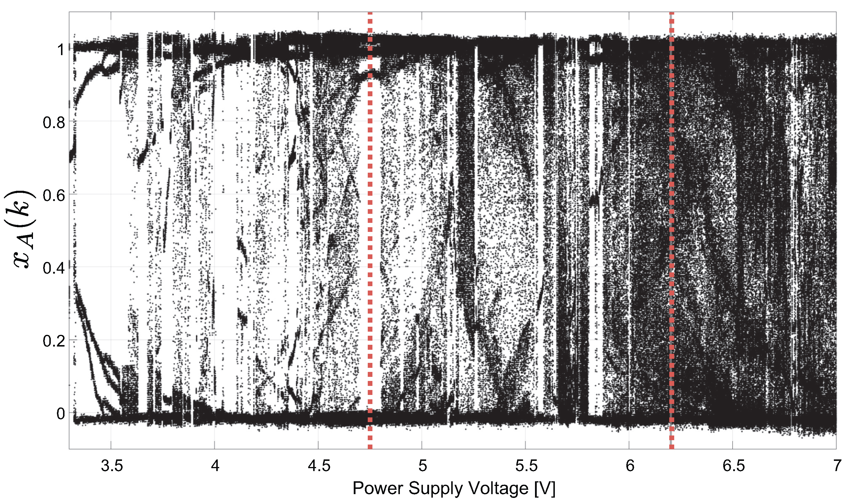
4. Overall DNO Circuit Analysis
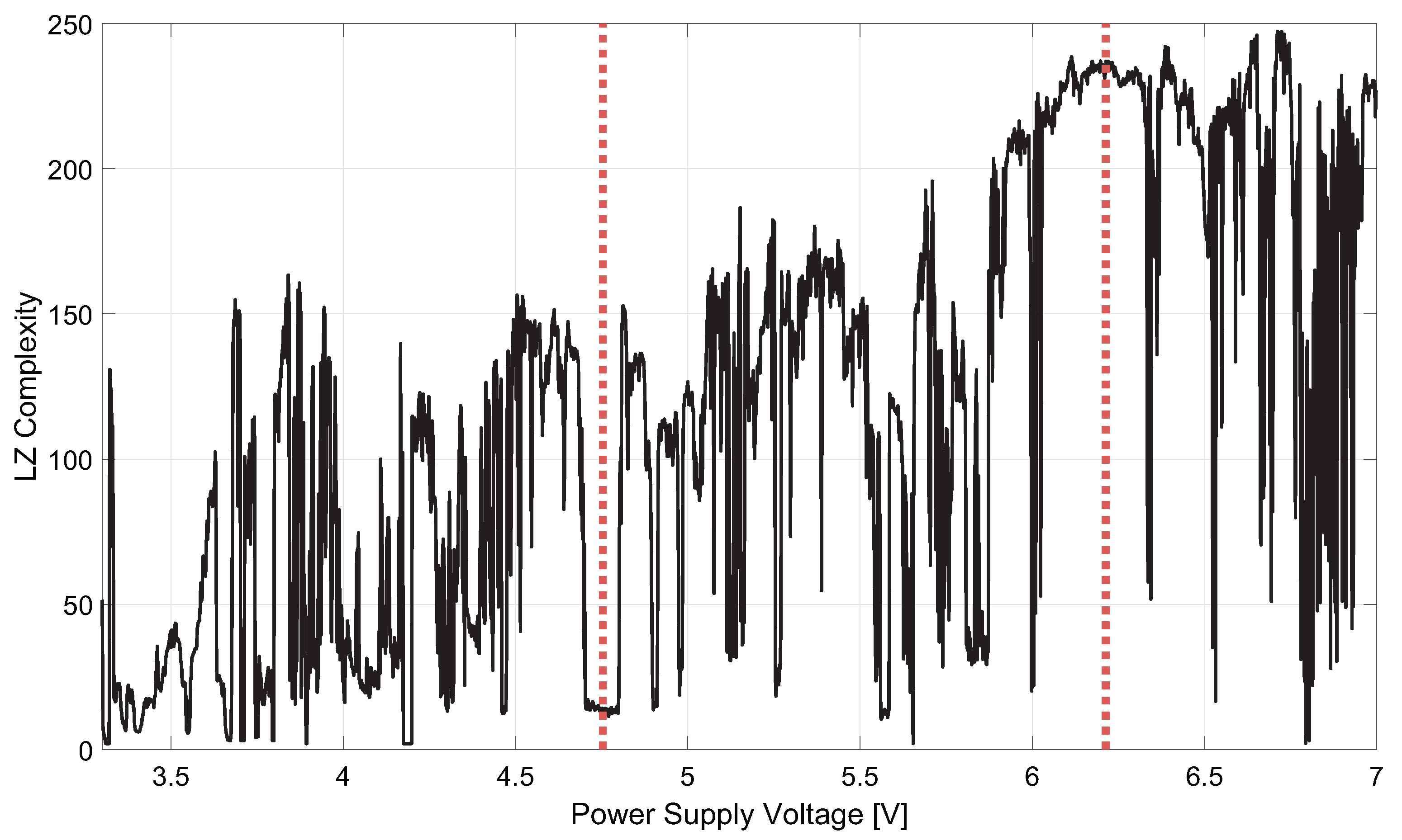
4.1. Randomness and Statistical Tests
5. Conclusions
Author Contributions
Funding
Data Availability Statement
Conflicts of Interest
References
- Addabbo, T.; Fort, A.; Moretti, R.; Mugnaini, M.; Takaloo, H.; Vignoli, V. A New Class of Digital Circuits for the Design of Entropy Sources in Programmable Logic. IEEE Trans. Circuits Syst. I Regul. Pap. 2020, 67, 2419–2430. [Google Scholar] [CrossRef]
- Golíc, J.D. New methods for digital generation and postprocessing of random data. IEEE Trans. Comput. 2006, 55, 1217–1229. [Google Scholar] [CrossRef]
- Addabbo, T.; Fort, A.; Moretti, R.; Mugnaini, M.; Vignoli, V.; Garcia Bosque, M. Lightweight True Random Bit Generators in PLDs: Figures of Merit and Performance Comparison. In Proceedings of the 2019 IEEE International Symposium on Circuits and Systems (ISCAS), Sapporo, Japan, 26–29 May 2019; pp. 1–5. [Google Scholar]
- Deng, D.; Hou, S.; Wang, Z.; Guo, Y. Configurable Ring Oscillator PUF Using Hybrid Logic Gates. IEEE Access 2020, 8, 161427–161437. [Google Scholar] [CrossRef]
- Addabbo, T.; Fort, A.; Mugnaini, M.; Vignoli, V.; Garcia-Bosque, M. Digital Nonlinear Oscillators in PLDs: Pitfalls and Open Perspectives for a Novel Class of True Random Number Generators. In Proceedings of the 2018 IEEE International Symposium on Circuits and Systems (ISCAS), Florence, Italy, 27–30 May 2018; pp. 1–5. [Google Scholar]
- Dang, T.K.; Serrano, R.; Hoang, T.T.; Pham, C.K. A Novel Ring Oscillator PUF for FPGA Based on Feedforward Ring Oscillators. In Proceedings of the 2022 19th International SoC Design Conference (ISOCC), Gangneung-si, Republic of Korea, 19–22 October 2022; pp. 87–88. [Google Scholar] [CrossRef]
- Li, T.; Wu, L.; Zhang, X.; Wu, X.; Zhou, J.; Wang, X. A novel transition effect ring oscillator based true random number generator for a security SoC. In Proceedings of the 2017 International Conference on Electron Devices and Solid-State Circuits (EDSSC), Hsinchu, Taiwan, 18–20 October 2017; pp. 1–2. [Google Scholar] [CrossRef]
- Kaysici, H.I.; Ergun, S. A Low Area Random Number Generator Based on Stability Changes of Ring Oscillators. In Proceedings of the 2021 IEEE International Midwest Symposium on Circuits and Systems (MWSCAS), Lansing, MI, USA, 9–11 August 2021; pp. 369–372. [Google Scholar] [CrossRef]
- Choi, S.; Shin, Y.; Yoo, H. Analysis of Ring-Oscillator-based True Random Number Generator on FPGAs. In Proceedings of the 2021 International Conference on Electronics, Information, and Communication (ICEIC), Jeju, Republic of Korea, 31 January–3 February 2021; pp. 1–3. [Google Scholar] [CrossRef]
- Wannaboon, C.; Ketthong, P. A Simple Random-Bit Generator Implemented on FPGA Based on Signum Chaotic Map. In Proceedings of the 2022 International Conference on Digital Government Technology and Innovation (DGTi-CON), Bangkok, Thailand, 24–25 March 2022; pp. 101–104. [Google Scholar] [CrossRef]
- Park, J.; Kim, B.; Sim, J.Y. A PVT-Tolerant Oscillation-Collapse-Based True Random Number Generator With an Odd Number of Inverter Stages. IEEE Trans. Circuits Syst. II Express Briefs 2022, 69, 4058–4062. [Google Scholar] [CrossRef]
- Cao, Y.; Liu, W.; Qin, L.; Liu, B.; Chen, S.; Ye, J.; Xia, X.; Wang, C. Entropy Sources Based on Silicon Chips: True Random Number Generator and Physical Unclonable Function. Entropy 2022, 24, 1566. [Google Scholar] [CrossRef] [PubMed]
- Garcia-Bosque, M.; Díez-Señorans, G.; Sánchez-Azqueta, C.; Celma, S. FPGA Implementation of a New PUF Based on Galois Ring Oscillators. In Proceedings of the 2021 IEEE 12th Latin America Symposium on Circuits and System (LASCAS), Arequipa, Peru, 21–24 February 2021; pp. 1–4. [Google Scholar] [CrossRef]
- Addabbo, T.; Fort, A.; Moretti, R.; Mugnaini, M.; Vignoli, V. Analysis of a Circuit Primitive for the Reliable Design of Digital Nonlinear Oscillators. In Proceedings of the 2019 15th Conference on Ph.D Research in Microelectronics and Electronics (PRIME), Lausanne, Switzerland, 15–18 July 2019; pp. 189–192. [Google Scholar]
- Vooke, K.; Toramamidi, N.K.; Thodeti, K.K.; Singh, S. Design of Pseudo-Random Number Generator Using Non-Linear Feedback Shift Register. In Proceedings of the 2022 First International Conference on Electrical, Electronics, Information and Communication Technologies (ICEEICT), Trichy, India, 16–18 February 2022; pp. 1–5. [Google Scholar] [CrossRef]
- Bak, P.; Bohr, T.; Jensen, M. Mode-locking and the transition to chaos in dissipative systems. Phys. Scr. 1985, 1985, 50–58. [Google Scholar] [CrossRef]
- Cveticanin, L. Forced pure nonlinear symmetrical oscillators. Math. Comput. Model. 2012, 55, 1580–1593. [Google Scholar] [CrossRef]
- Miwadinou, C.; Monwanou, A.; Yovogan, J.; Hinvi, L.; Tuwa, P.N.; Orou, J.C. Modeling nonlinear dissipative chemical dynamics by a forced modified Van der Pol-Duffing oscillator with asymmetric potential: Chaotic behaviors predictions. Chin. J. Phys. 2018, 56, 1089–1104. [Google Scholar] [CrossRef]
- Ainamon, C.; Miwadinou, c.; Monwanou, A.; Orou, J. Analysis of Multiresonance and Chaotic Behavior of the Polarization in Materials Modeled by a Duffing Equation with Multifrequency Excitations. Appl. Phys. Res. 2014, 6, 74–86. [Google Scholar] [CrossRef]
- Bashkirtseva, I.; Ryashko, L. Sensitivity and chaos control for the forced nonlinear oscillations. Chaos Solitons Fractals 2005, 26, 1437–1451. [Google Scholar] [CrossRef]
- Mandal, M.; Sarkar, B.C. Ring oscillators: Characteristics and applications. Indian J. Pure Appl. Phys. 2010, 48, 136–145. [Google Scholar]
- Ramazani, A.; Biabani, S.; Hadidi, G. CMOS ring oscillator with combined delay stages. AEU—Int. J. Electron. Commun. 2014, 68, 515–519. [Google Scholar] [CrossRef]
- Kumar, R.; Kursun, V. Impact of temperature fluctuations on circuit characteristics in 180nm and 65nm CMOS technologies. In Proceedings of the 2006 IEEE International Symposium on Circuits and Systems, Kos, Greece, 21–24 May 2006. [Google Scholar] [CrossRef]
- Afentakis, T.; Hatalis, M. A simple analytical model for the dependence of the propagation delay of the polycrystalline silicon CMOS inverter on temperature. Solid-State Electron. 2002, 46, 2301–2306. [Google Scholar] [CrossRef]
- Kalra, S. Effect of temperature dependence on performance of Digital CMOS circuit technologies. In Proceedings of the 2013 International Conference on Signal Processing and Communication (ICSC), Noida, India, 12–14 December 2013; pp. 392–395. [Google Scholar] [CrossRef]
- Lempel, A.; Ziv, J. On the Complexity of Finite Sequences. IEEE Trans. Inf. Theory 1976, 22, 75–81. [Google Scholar] [CrossRef]
- Rukhin, A.; Soto, J.; Nechvatal, J.; Smid, M.; Barker, E. A Statistical Test Suite for Random and Pseudorandom Number Generators for Cryptographic Applications; Booz-Allen and Hamilton Inc.: McLean, VA, USA, 2001. [Google Scholar]


| Test Name | p-Value | Proportion | Result |
|---|---|---|---|
| Frequency | 0.897763 | 1.00 | pass |
| BlockFrequency | 0.719747 | 0.97 | pass |
| CumulativeSums | 0.637119 | 0.99 | pass |
| Runs | 0.514124 | 0.96 | pass |
| LongestRun | 0.455937 | 0.99 | pass |
| Rank | 0.042808 | 1.00 | pass |
| FFT | 0.657933 | 0.97 | pass |
| NonOverlappingTemplate | 0.739918 | 0.96 | pass |
| OverlappingTemplate | 0.851383 | 0.99 | pass |
| Universal | 0.595549 | 0.97 | pass |
| ApproximateEntropy | 0.030806 | 0.99 | pass |
| RandomExcursions | 0.051391 | 0.97 | pass |
| RandomExcursionsVariant | 0.116519 | 0.98 | pass |
| Serial | 0.275709 | 0.99 | pass |
| LinearComplexity | 0.102526 | 0.99 | pass |
Disclaimer/Publisher’s Note: The statements, opinions and data contained in all publications are solely those of the individual author(s) and contributor(s) and not of MDPI and/or the editor(s). MDPI and/or the editor(s) disclaim responsibility for any injury to people or property resulting from any ideas, methods, instructions or products referred to in the content. |
© 2023 by the authors. Licensee MDPI, Basel, Switzerland. This article is an open access article distributed under the terms and conditions of the Creative Commons Attribution (CC BY) license (https://creativecommons.org/licenses/by/4.0/).
Share and Cite
Addabbo, T.; Fort, A.; Moretti, R.; Spinelli, F.; Vignoli, V. Complex Dynamics in Digital Nonlinear Oscillators: Experimental Analysis and Verification. Electronics 2023, 12, 2459. https://doi.org/10.3390/electronics12112459
Addabbo T, Fort A, Moretti R, Spinelli F, Vignoli V. Complex Dynamics in Digital Nonlinear Oscillators: Experimental Analysis and Verification. Electronics. 2023; 12(11):2459. https://doi.org/10.3390/electronics12112459
Chicago/Turabian StyleAddabbo, Tommaso, Ada Fort, Riccardo Moretti, Filippo Spinelli, and Valerio Vignoli. 2023. "Complex Dynamics in Digital Nonlinear Oscillators: Experimental Analysis and Verification" Electronics 12, no. 11: 2459. https://doi.org/10.3390/electronics12112459