Article

A High-Power Density DC Converter for Medium-Voltage DC Distribution Networks

1
State Grid Hunan Electric Power Company Limited Research Institute, Changsha 410007, China
2
National Engineering Research Center for Electrical Energy Conversion and Control, Hunan University, Changsha 410082, China
*
Author to whom correspondence should be addressed.
Electronics 2023, 12(18), 3975; https://doi.org/10.3390/electronics12183975
Submission received: 22 August 2023 / Revised: 14 September 2023 / Accepted: 18 September 2023 / Published: 21 September 2023

Abstract

:
A DC converter is the core equipment of voltage conversion and power distribution in a DC distribution network. Its operating characteristics have a profound impact on the flexible regulation of distributed resources in an active distribution network. It is challenging for the existing single-stage conversion topology to meet the requirements of distributed renewable energy connected to a multi-voltage level, medium-voltage grid. It is necessary to study the multistage transform power unit topology further, which can satisfy high reliability, high efficiency, and wide input range. This paper proposes a high-power density DC converter for medium-voltage DC networks with wide voltage levels. It adopts Buck-LLC integrated modular composition. The input ends of the high isolation resonant power unit are connected in series to provide high voltage endurance, and the output ends are connected in parallel to meet the high-power demand and achieve high-power transmission efficiency. The proposed series dual Buck-LLC resonant power unit topology can adjust the duty cycle of series dual buck circuits to meet the needs of different levels of medium-voltage DC power grids. The soft switching problem within the wide input range of all switching tubes is solved by introducing auxiliary inductors, thereby improving energy transmission efficiency. The auxiliary circuit and control parameters are optimized based on the research of each switching tube’s soft switching boundary conditions. Finally, an experimental prototype of a 6.25~7 kW power unit is designed and developed to prove the proposed topology’s feasibility and effectiveness. Great breakthroughs have been made both in theoretical research and engineering prototype development.

1. Introduction

With the large-scale penetration of renewable energies, storage, and various types of power electronic devices in recent years, the construction of a new power system with renewable energy as the main body has attracted wide attention. Flexible DC distribution network technology, with high-power quality, high stability, and flexible control advantages, has become a research hotspot [1,2,3,4,5]. Among them, the DC transformer is indispensable as the hub of energy convergence and distribution in the DC power grid.
Unlike the AC transformer, through the electromagnetic induction voltage conversion principle, the DC transformer can only use power electronic devices to achieve DC voltage manipulation. Some DC converter topologies have been mature applications, but not all topologies meet the connection needs of different medium voltage levels. A clamp multilevel circuit was first introduced by A. Nabae et al. [6], in which a midpoint clamp topology is proposed. The voltage stress of each device is only half of the DC side voltage. It has been widely used in high-voltage and high-power situations. However, with the voltage levels increasing, the number of power devices also increases, and the number of diodes increases by the square of the voltage levels. Therefore, the current practical application is mainly a three-level structure, which limits the voltage level of its application to generally less than 3 kV [7,8].
The concept of a modular multilevel structure was first proposed in 2001 by Rainer Marquardt, a scholar at the Bundeswehr University in Munich, Germany. The modular multilevel converter (MMC) adopts the cascade of sub-modules of half-bridge and full-bridge converter structures, which does not have the problems of dynamic voltage equalization and consistent triggering. It has been widely studied and applied in flexible DC transmission [9,10,11,12,13,14,15]. In [16], a compact MMC-DC/DC is proposed, which improves the integration of MMC-DC/DC, but the short-circuit fault on the DC side is not considered. When the DC side is short-circuited, a large number of submodule capacitors are short-circuited and discharged, resulting in a large short-circuit impulse current that endangers the safe operation of the transmission line. Thus, Professor Hui Li of Florida State University proposed the improved current source type MMC-DC/DC topology [17,18]. The bridge arm inductor is added based on the full-bridge submodule type MMC structure, and the high-frequency conversion port between the bridge arm inductor is led out. When there is a short-circuit fault on the DC side, the bridge arm inductor can limit the fault current well, and the whole bridge submodule can realize the DC side fault crossing.
The resonant converter and MMC topology combination have also received more and more attention in medium-voltage DC research [19]. A transformer-free resonant modular multilevel converter is proposed in [20], with inherent voltage-balance capability between modules. Moreover, it adopts phase-shift control between modules to obtain higher equivalent switching frequency and step-down ratios. However, the switching tube’s high voltage and current stress limit its application in high-voltage and high-power situations. In addition, the lack of electrical isolation limits its potential for further expansion. Therefore, [21] added isolation transformers to the topology, which can achieve electrical isolation and bidirectional energy flow. The voltage gain can also be manipulated by adjusting the number of submodules involved in modulation.
In the modular combined DC converter, [22] describes the connection mode of a modular combined converter in detail. It puts forward the general control method of four series-parallel combined systems. In [23], the modular combined DC converter’s operation characteristics and control methods are deeply studied, which is used to interconnect high and low-voltage DC power grids. In [24], the research of modular combined DC converters in flexible DC distribution is carried out. In [25], the modular combined DC converter is improved, and a topology based on four active full-bridge power modules is proposed. Due to its modular structure, high-frequency isolation, and other characteristics, modular combined DC converters have also been widely studied in AC-DC power electronic transformers [26,27,28].
In summary, the ISOP structure suits high-voltage and low-voltage output in medium-voltage conversion. The modular power unit can realize topology integration with a simple structure. It also has an immense capacity-expansion ability and can fully reflect the advantages of the power unit topology. Moreover, it can improve reliability, which is more suitable for the scenario of renewable energy access studied in this paper. However, with access requirements for broad voltage levels in medium-voltage power grids, single-stage conversion power units can hardly meet the criteria mentioned. The multistage conversion power unit topology with high reliability, high efficiency, and wide input range is required.
This paper proposes a Buck-LLC integrated modular combined DC converter for renewable energy access. A detailed analysis of the converter operating principles is performed to illustrate the features. A comparison with the current existing references and the proposed converter is presented in Table 1.
Based on the analysis of the working principle of the proposed topology, its DC gain characteristics, power characteristics, and soft switch characteristics were derived. The boundary conditions of soft switching for each switch tube were studied. The auxiliary circuit and control parameters were optimized and designed. The experimental results of the prototype verify the analysis, as mentioned above.

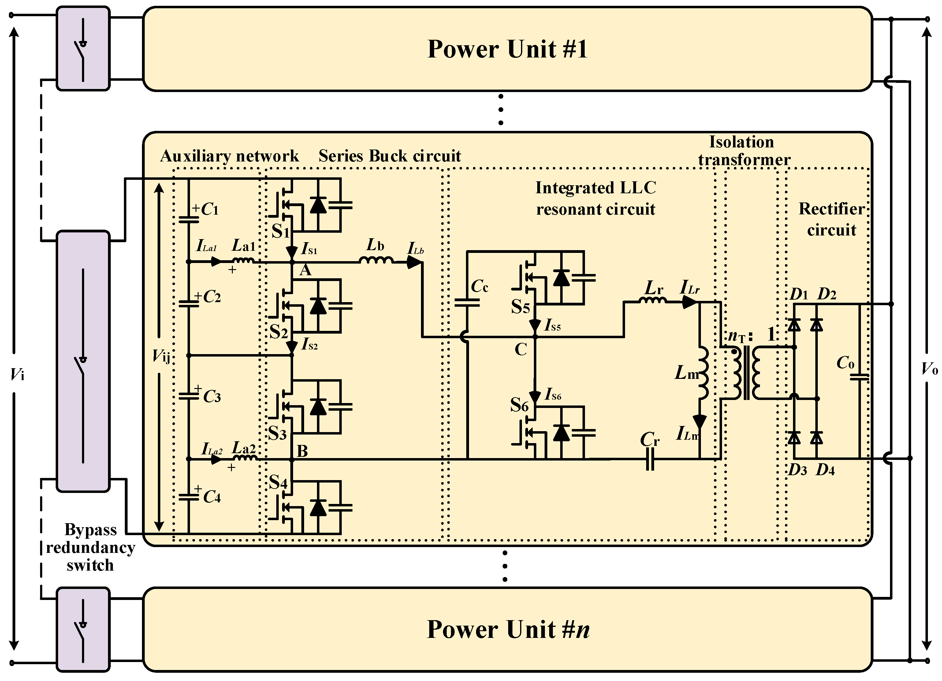
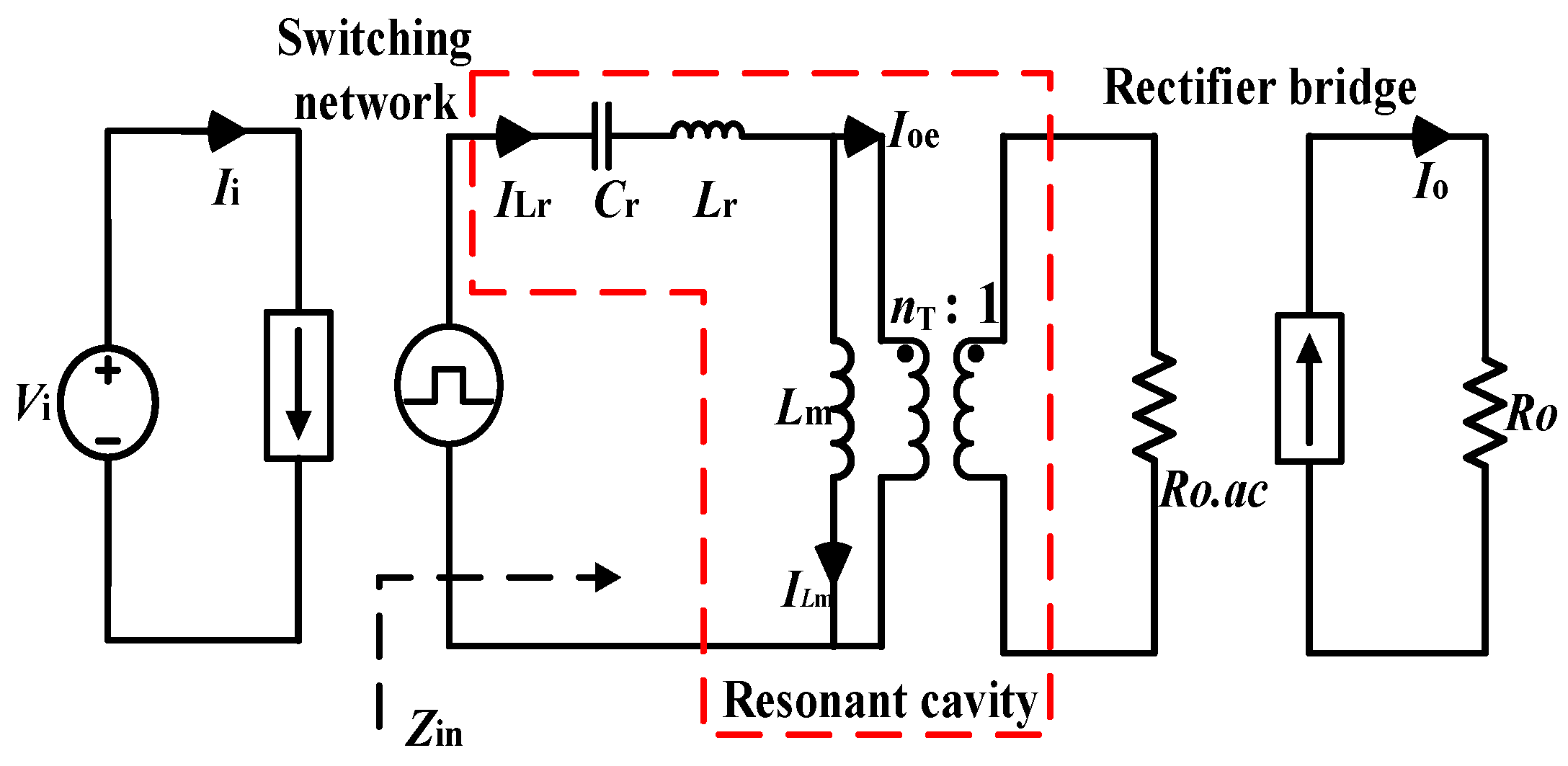
2. Modular Combined DC Converter Topology Based on Buck-LLC Integration

The modular combined DC converter based on Buck-LLC integration in this paper is shown in Figure 1. A series dual-buck integrated LLC converter (SDBuck-LLC) is used as a power unit. The input terminals of each power unit bear high voltage in series and output terminals in parallel to provide stable DC output. Considering the redundancy requirements of power units, redundant switches are connected to the input front of each power unit, which has the advantages of quick cutting of power units, fault current limiting, etc.
The above SDBuck-LLC comprises an auxiliary network, series buck circuit, integrated LLC resonant circuit, isolation transformer, and rectifier circuit. The converter uses high-frequency SiC MOSFET S1~S6 as the main power switch tubes to meet the stable operation at the high-input voltage operating point. Moreover, all switch tubes can realize soft switching in a wide working range. The buck circuit uses S1~S4 as the power switches, withstanding the high input voltage stress in series, and realizes the voltage reduction through the previous stage circuit. The S5 and S6 are switching tubes in the rear LLC resonant circuit, providing convenience for each switching tube’s ZVS through the resonator. Input capacitors C1~C4 and auxiliary inductors La1 and La2 form an auxiliary network to provide a bias current for S1~S4 to meet the conditions of realizing ZVS. As the output inductor of the series buck circuit, Lb is connected with1 S2 and S1 at point A and S5 and S6 at point C.
The clamping capacitor Cc, S5, and S6 together form an integrated half-bridge circuit, which can not only work with the front-end buck inductor Lb to adjust the clamping capacitor voltage VCc, but also form a half-bridge resonant circuit with the back-end cavity. The resonator cavity comprises the resonant inductor Lr, the resonant capacitor Cr, the excitation inductor Lm, and the high-frequency isolation transformer. The isolation transformer is used to realize the electrical isolation of the input and output terminals, and then the required low-voltage DC is obtained by the rectifier diode D1~D4 rectification. The transformer ratio is nT:1. ILf, ILr, ILb, ILa1, ILa2 are the current flowing through the inductor Lf, Lr, Lb, La1, and La2, respectively. The forward reference direction of the currents is given in the form of an arrow in Figure 1.

3. SDBuck-LLC’s Operating Principle and Steady-State Analysis

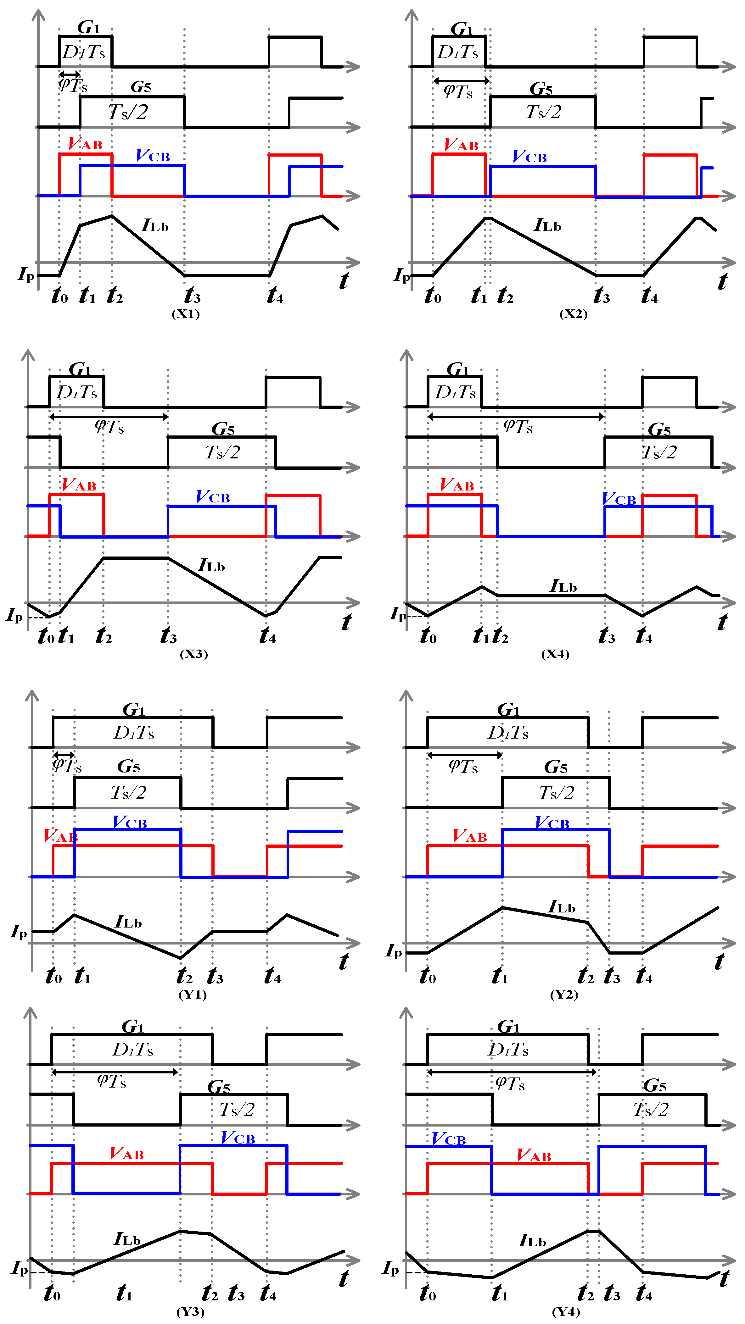
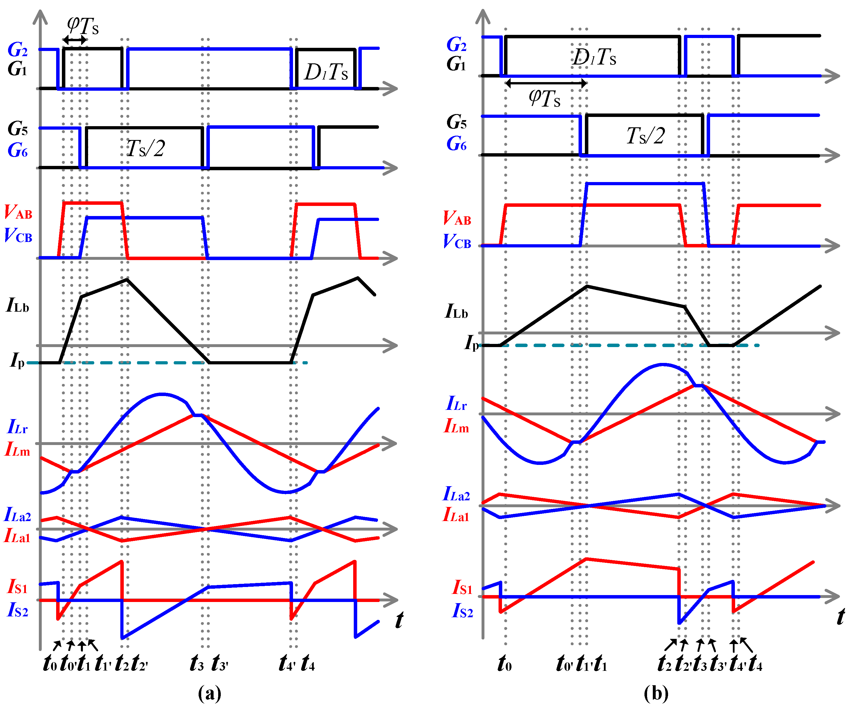
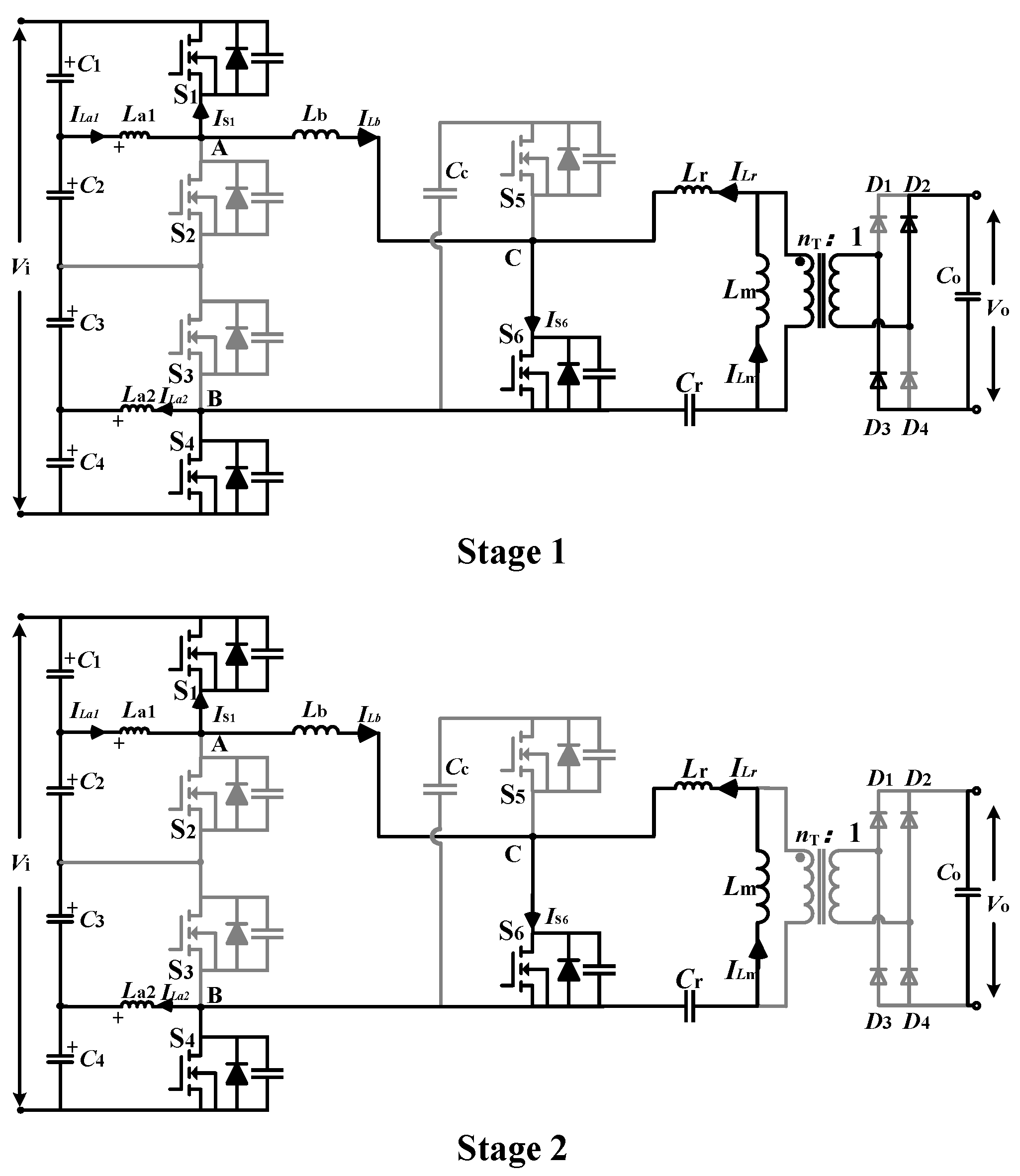
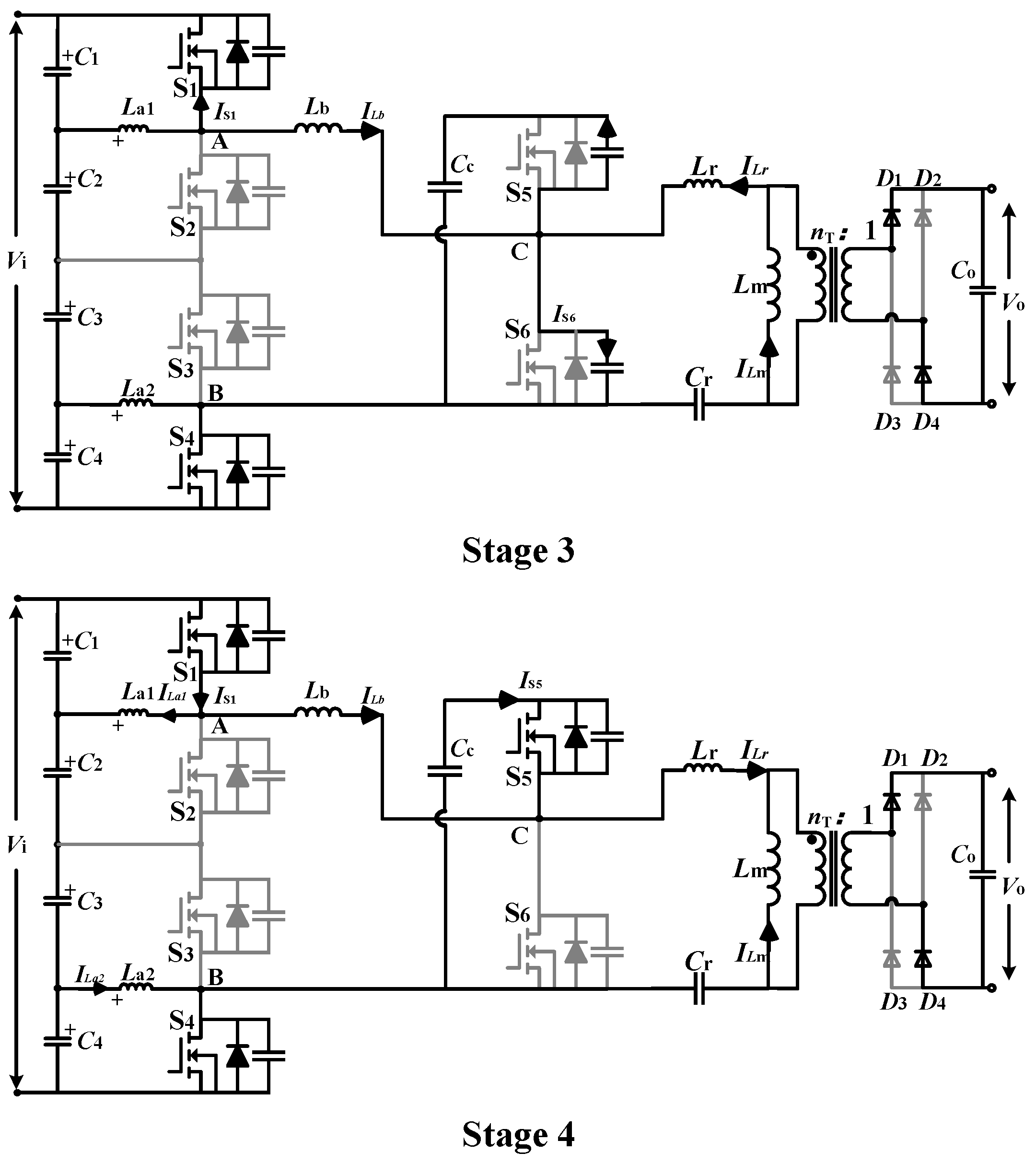
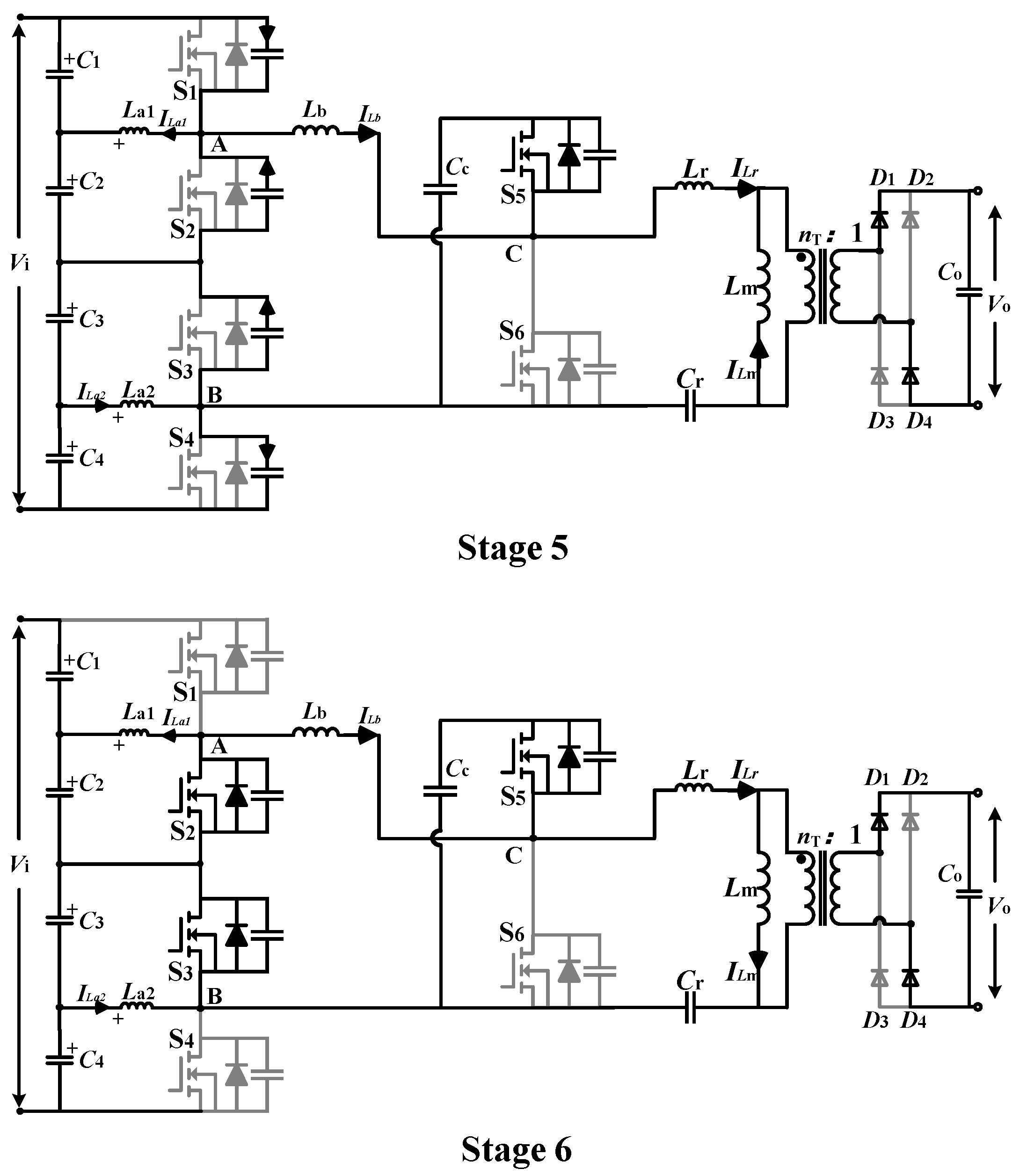
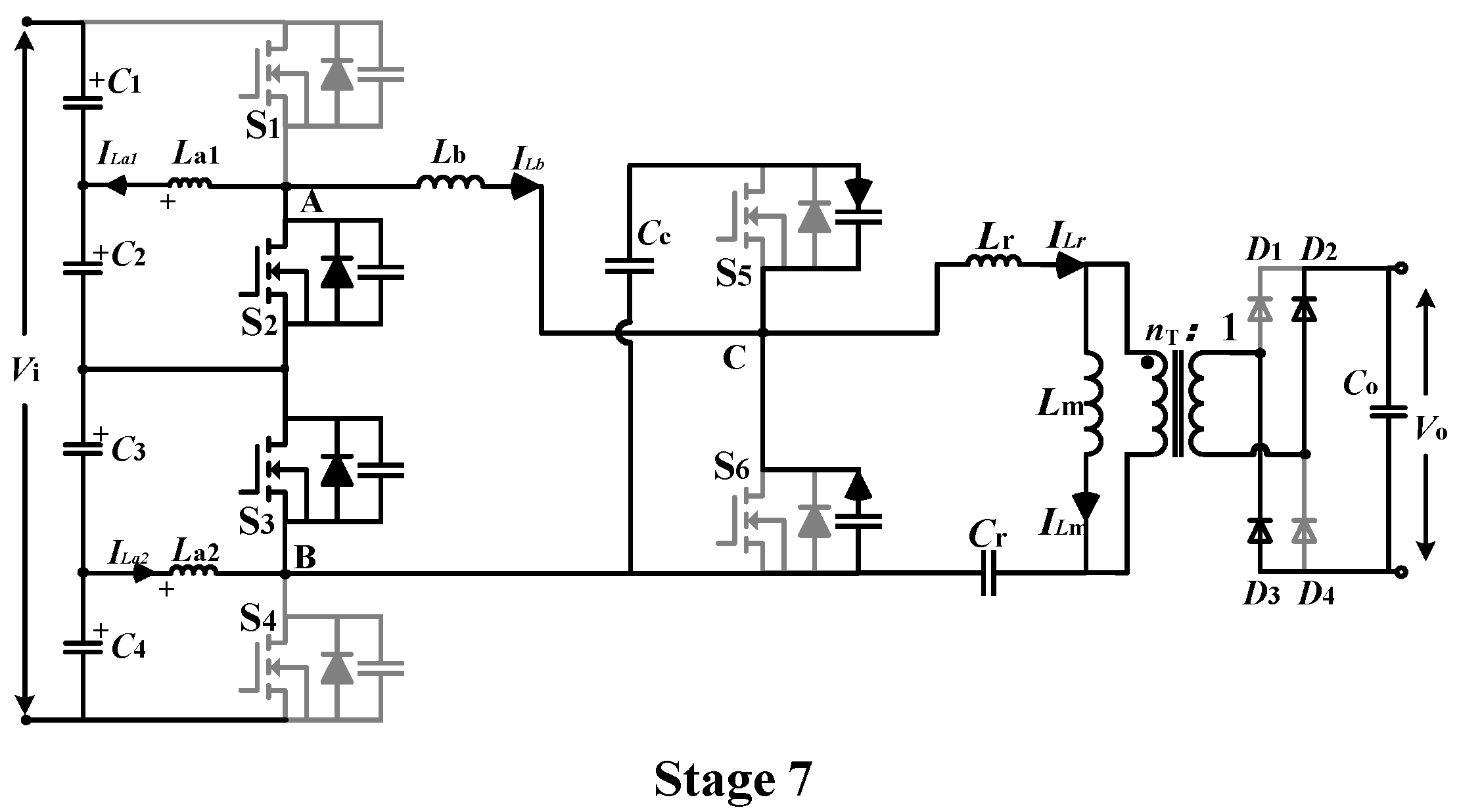
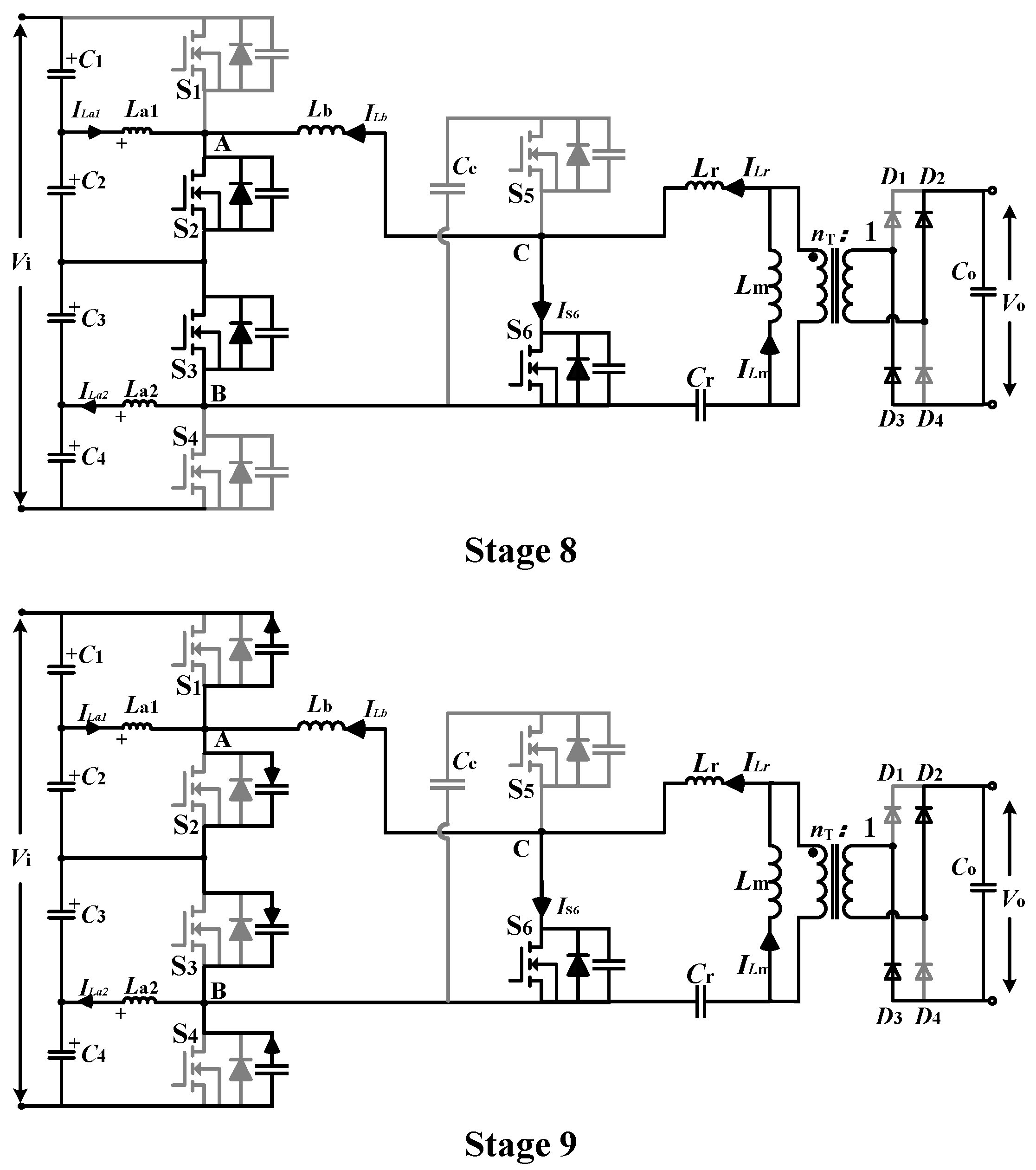
3.1. Analysis of Working Mode and Working Principle

The power unit SDBuck-LLC adopts a fixed-frequency and fixed-phase-shift pulse-width modulation strategy and adjusts the output voltage by controlling the duty cycle of S1~S4 in the series buck circuit. The phase-shift angle between S1 and S5 and the auxiliary network provides appropriate current bias to ensure all switching tubes can realize ZVS within a wide input voltage range. LLC resonators operate at a fixed frequency. Specifically, the driving signals G1 and G4 of switching tubes S1 and S4 are the same, and the duty cycle is D1; the driving signals G2 and G3 of the switching tube S2 and S3 are the same. S1 and S2 are complementary switching on. The duty cycle D2 of the switching tube S5 is fixed at 0.5. S5 and S6 are complementary switching on. Define G1 rising edge leading G5 rising edge φTs.
By analyzing the relationship between D1 and φ, the working state of the converter can be divided into eight working modes, as shown in Table 2, and the brief waveform of each working mode is shown in Figure 2.
To ensure that the switching tube S1~S6 could meet the ZVS condition under various load conditions within a wide input voltage range, the buck inductor current ILb should be negative at the turn-on time of S1, S4, and S6. The modes X4 and Y1 could not meet the current requirements above. Thus, modes X4 and Y1 are not included in the working range of the power unit. The proposed power unit adopts the fixed frequency and fixed phase-shift control scheme. To adapt to the power transmission in a wide range, the phase shift φTs should not be too significant.
Thus, mode X3, mode Y3, and mode Y4 are excluded. In mode X2, D1 < φ, the inductor Lb has two continuous current states in one cycle. Compared with mode X1, the RMS value of the buck inductor current ILb in mode X2 is slightly higher under the same voltage gain, transmission power, and ZVS conditions. Thus, Mode X2 will lead to higher loss. In summary, mode X1 and mode Y2 are the most suitable operating modes for the proposed SDBuck-LLC within the design requirements. Therefore, the two working modes are analyzed in detail in this paper. The critical waveforms of each mode are shown in Figure 3, and the corresponding equivalent circuits are shown in Figure 4, Figure 5, Figure 6 and Figure 7. For simple analysis, two assumptions are followed: (1) all devices, including switching tubes and capacitors, are ideal devices; and (2) the DC voltage ripple at both ends of the output capacitor is ignored.
(1) Mode X1:
Stage 1 (t0~t0′): Before time t0, S6 has been turned on. The driving signals G1, G4 of S1, and S4 rise at time t0. Since the reverse diodes of S1 and S4 have been switched on, S1 and S4 realize ZVS, and VAB rises from 0 to Vi. At this stage, the voltage of the auxiliary inductors La1 and L a2 is -Vc1 and Vc4, which are both in the discharge and charging states, respectively. The input voltage VCB of the resonator is 0, and the voltage applied at both ends of the buck inductor Lb is the difference between VAB and VCB, which is equal to Vi. Lb is in a state of high excitation, and ILb rises rapidly from the initial Ip value. The resonant current ILr increases by a sine wave at the resonant frequency fr. The diodes D2 and D3 are on. The excitation inductor voltage VLm is clamped by the reverse output voltage Vo, and the excitation inductor current ILm gradually decreases.
Stage 2 (t0′~t1): At t0′, ILr equals ILm. Diodes D1~D4 are turned off at this stage, and no current passes through the transformer winding. No energy is transmitted to the secondary side through the transformer. The resonant inductor Lr, the excitation inductor Lm, and the resonant capacitor C, participate in the resonance, and the resonant frequency is fm. Because the excitation inductor is higher than the resonant inductor in the LLC resonant design, the change of resonant current at this stage is minimal.
Stage 3 (t1~t1′): At t1, S6 is turned off, and S1 and S4 remain on. This phase is the dead time between S6 and S5. The junction capacitors of S5 and S6 begin to discharge and charge, respectively, laying the foundation for the ZVS of S5. At the same time, D1 and D4 switch on, and the excitation inductor Lm exits the resonance link.
Stage 4 (t1′~t2): At t1′, the driving signal G5 of S5 begins to rise, then S5 realizes ZVS, and the current value passing through S5 at the opening moment is the difference between ILr and ILb. The input voltage VCB of the resonator rises and equals the clamp capacitor voltage VCc. The voltage applied at both ends of Lb equals ViVCc, Lb is in a low excitation state, and the growth rate of ILb slows down. The auxiliary inductor currents I La1 and I La2 fall and rise simultaneously, but the direction reverses at this stage. In the resonator cavity, only the resonator inductor and the resonator capacitor participate in the resonance. ILr increases with the resonant frequency fr as a sine wave, VLm is affected by Vo clamp, and ILm gradually increases.
Stage 5 (t2~t2′): at t2, S1 is turned off and S5 remains open. ILa1 and ILa2, respectively, reach the lowest and highest values. This phase is the dead time between S2 and S1, and the junction capacitors of S1 and S2 begin to charge and discharge, respectively, providing conditions for the ZVS of S2.
Stage 6 (t2′~t3): at t2′, the driving signal G2 of S2 rises, and then S2 realizes ZVS. The current value passing through S2 at the opening moment is the difference between I Lra1 and ILb. VAB drops to 0, and the voltage applied at both ends of Lb equals -VCc, which is in a deep demagnetization state. ILb drops rapidly. The voltage applied in the ports of La1 and La2 is Vc2 and -Vc3, respectively, in the charging and discharging state. In this stage, the resonator resonates at two resonant frequencies, fr and fm. The condition of resonant frequency fm is like that of the above stage 2.
Stage 7 (t3~t3′): at t3, S5 is turned off, S2 and S3 remain on, and the dead time between S5 and S6 is entered again. Then, the junction capacitors of S5 and S6 begin to charge and discharge, respectively, providing conditions for the ZVS of S6. At the same time, in this stage, the rectifier bridge starts to reverse pilot, and the excitation inductor Lm exits the resonant link.
Stage 8 (t3′~t4′): at t3′, the driving signal G6 of S6 rises, and then S6 realizes ZVS. The current value passing through S6 at the opening moment is the difference between the inductor current ILb and the resonant current ILr. The input voltage VCB of the resonator drops to 0. The voltage applied at both ends of Lb is 0, and Lb is in the continuous current state. ILb remains unchanged. The rising and falling rates of ILa1 and ILa2 remain the same, but the direction reverses at this stage. In the resonator cavity, only the resonant inductor and the resonant capacitor participate in the resonance. The resonant current ILr decreases as a sine wave with the resonant frequency fr. The excitation inductor voltage VLm is affected by the reverse output voltage Vo clamp, and ILm gradually decreases.
Stage 9 (t4′~t4): at t4′, S2 is turned off, S6 remains open, and ILa1 and ILa2 reach the highest and lowest values, respectively. The dead time between S2 and S1 starts again. The junction capacitors of S1 and S2 begin to discharge and charge, respectively. At t4, the driving signal of S1 rises, and S1 realizes ZVS. The current value passing through S1 at the opening moment is the difference between ILb and ILa1; then, the next cycle is entered.
(2) Mode Y2:
The proposed power unit SDBuck-LLC works in mode Y2 roughly the same as in mode X1. The main differences are as follows:
(a)
In stage 4 of mode Y2, the voltage applied at both ends of Lb is Vi-VCc, which is negative at this time, in a low demagnetization state, and ILb slowly decreases.
(b)
The deep excitation state time corresponding to stages 1, 2, and 3 is lengthened, and the resonant negative half-cycle corresponding to this period is also lengthened.
(c)
The deep demagnetization state time corresponding to stages 6 and 7 is shortened, and the resonant positive half-period corresponding to this period is also shortened.

3.2. Characteristics of DC Voltage Gain

The presence of the auxiliary network shown in Figure 1 does not affect the voltage gain of each mode of the power unit, and the overall gain of the converter can be obtained by analyzing the two-stage converter gain separately. Define MBuck as the DC gain of the front-stage buck converter and MLLC as the DC gain of the back-stage half-bridge LLC resonant converter; then, the gain of the power unit is:
M dc = M Buck M LLC
Through the above modal analysis, VAB is a square wave with a duty cycle of D1 and an amplitude of Vi. VCB is a square wave with a duty cycle of 0.5 and an amplitude of VCc. For buck inductor Lb, according to the volt-second balance principle, it can be obtained:
D 1 V i = ( 1 0.5 ) V cc
Namely:
M B u c k = V C c / V i = 2 D 1
Based on fundamental wave analysis, the steady-state equivalent circuit of the SDBuck-LLC resonant converter studied in this paper is shown in Figure 8.
First, the following parameter definitions are listed below:
Equivalent   resistance   R eq :   R e q = n T 2 R o . a c = 8 n T 2 π 2 R o
Quality   Factor   Q :   Q = 1 R eq L r C r
Normalized   frequency   f n :   f n = f s / f s n
Inductance   coefficient   λ :   λ = L r / L m
Resonant   angular   ω r :   ω r = 1 L r C r
According to the steady-state equivalent circuit shown in Figure 8, the input impedance Zin can be calculated by Equation (9).
Z i n ( j ω ) = j h ω L r j h ω C r + j h ω L m / / R e q
The transfer function of the h harmonic of the resonator can be calculated by Equation (10).
H h ( j ω ) = 1 n T j h ω L m / / R e q ( j h ω L m / / R e q ) + j h ω L r j h ω C r
Therefore, the gain MLLC of the half-bridge LLC resonant circuit can be obtained in Equation (11).
M L L C = V O V Cc = 1 2 H 1 ( j 2 π f e ) = 1 2 n T ( 1 + λ λ f n 2 ) 2 + Q 2 ( f n 1 f n ) 2
LLC resonant converters mainly adjust the output voltage by changing the switching frequency. Thus, a wide input voltage range corresponds to a wide switching frequency adjustment range, reducing the converter efficiency. In practical application, for ZVS realization and efficiency improvement, the switching frequency of the switching tube should be near the resonant frequency fr as far as possible. Thus, MLLC is 0.5. The integrated converter proposed in this paper works at the resonant frequency point.
In summary, the ideal DC gain of the SDBuck-LLC converter is:
M dc = D 1 n T

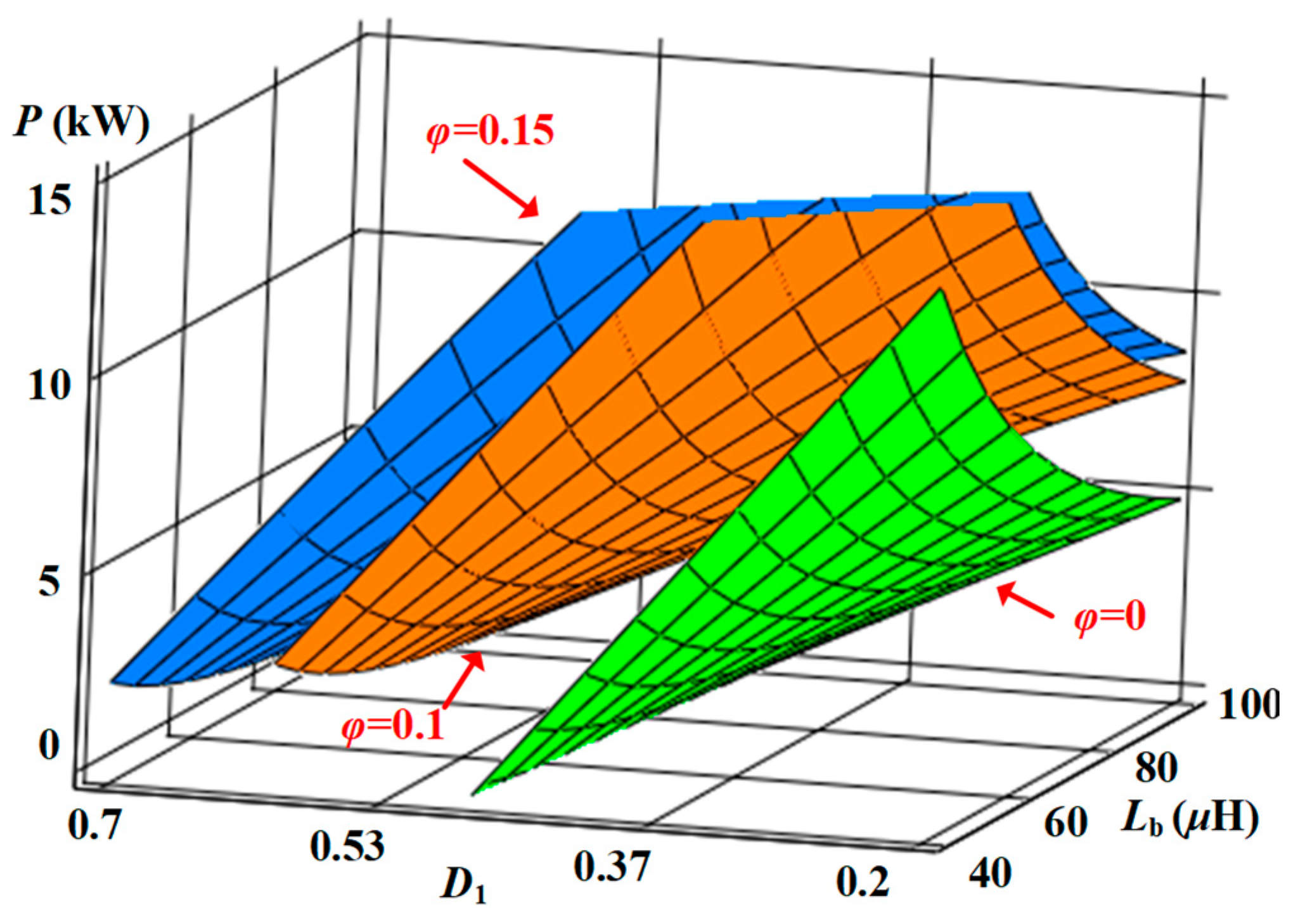
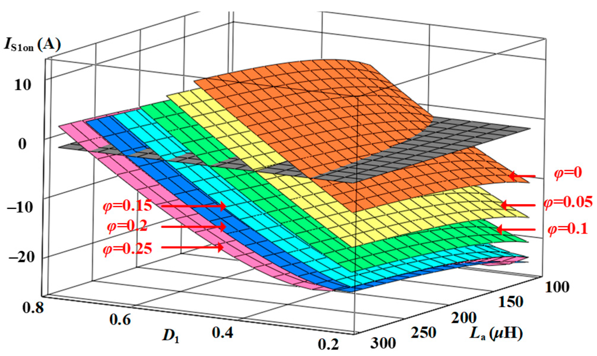
3.3. Voltage Stress and Power Characteristics

The voltage stress of a power device is one of the critical theoretical bases for its selection. Based on the modal analysis of mode X1, the power unit’s voltage stress of each power device is described in detail. In stage 1 and stage 2, the switching tubes S1, S6, S4, and inductor Lb form a loop with the input end, and the output diode D2 and D3 are on. The switching tube S2 and S3 need to jointly withstand the input voltage Vi, and the voltage at both ends of the inductor Lb is also Vi. The diode D1 and D4 must withstand the output voltage Vo, and the switching tube S5 must withstand the capacitor voltage VCc.
In stage 6, the switch tube S2, S3, S5, buck inductor Lb, and capacitor Cc form a voltage loop, and the output diodes D1 and D4 are on. The switching tubes S1 and S4 must withstand the input voltage Vi jointly, and the voltage at both ends of the inductor Lb is VCc. The diode D2 and D3 must withstand the output voltage Vo, and the switch tube S6 must withstand the capacitor voltage VCc.
Therefore, the voltage stress of the switching tube S1~S4 is:
V S 1 - max = V S 2 - max = V S 3 - max = V S 4 - max = V i / 2
The voltage stress of the switching tube S5, S6 is:
V S 5 - max = V S 6 - max = V Cc = 2 D 1 V i
The voltage stress of diode D1~D4 is:
V D 1 - max = V D 2 - max = V D 3 - max = V D 4 - max = V o = D 1 V i
According to the above modal analysis, the current expression of inductor Lb in mode X1, Y2 can be obtained as follows; Ip is the current value of the buck inductor when S1 is turned on, and it is also the minimum current value in its cycle.
I Lb - X 1 Y 2 ( t ) = { I p + V i t / L b I p + ( V Cc φ T s + ( V i V Cc ) t ) / L b I p + ( V Cc φ T s + V i D 1 T s V Cc t ) / L b I p 0 t φ T s φ T s t D 1 T s D 1 T s t ( φ + 0.5 ) T s ( φ + 0.5 ) T s t T s
It shows that the inductance Lb and phase-shift angle affect the inductor current’s peak value. The larger the inductance Lb, the smaller the peak value of inductance current and its effective value, and the smaller the on-loss of the converter.
P i = P o = 1 T s t 0 t 4 V AB ( t ) I Lb ( t ) d t = 1 T s t 0 t 4 V CD ( t ) I Lb ( t ) d t
P X 1 Y 2 = 0.5 I p V Cc + V Cc 2 T s 4 L b ( φ 2 D 1 + 2 φ D 1 + 0.5 )
According to Equation (17), the transmission power of the converter under the ideal conditions of mode X1, Y2 can be obtained, as shown in Equation (18).
It can be seen from the above equations that P, Ip, D1, and φ are mutually restricted under the premise that the other parameters of the converter device are determined. When the input voltage is determined, the duty cycle D1 is also determined, and Ip is closely related to the transmission power P and phase shift φTs.
Figure 9 shows the relationship between output power P, duty cycle D1, and inductance Lb under different phase shifts φTs when fs = 80 k, Vo = 400 V, and Ip = 3 A in modes X1 and Y2. Obviously, with the increase in phase shift φTs, the modes X1 and Y2 of the converter gradually tend to work at a higher duty cycle, and the power that can be transmitted also increases. Moreover, the value of inductance Lb also affects the power that can be transmitted; the more significant the Lb, the weaker the power transmission capacity.

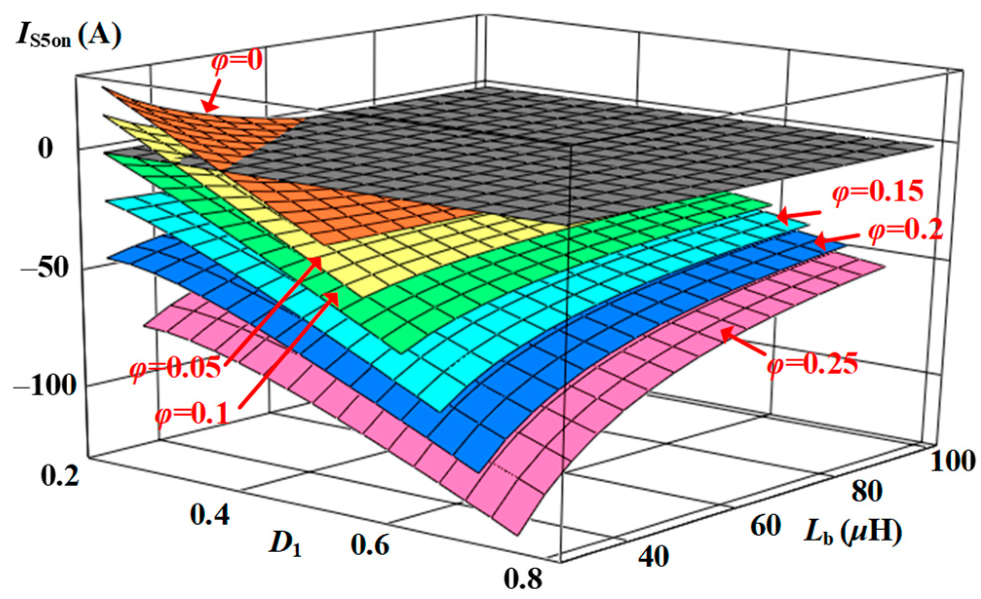
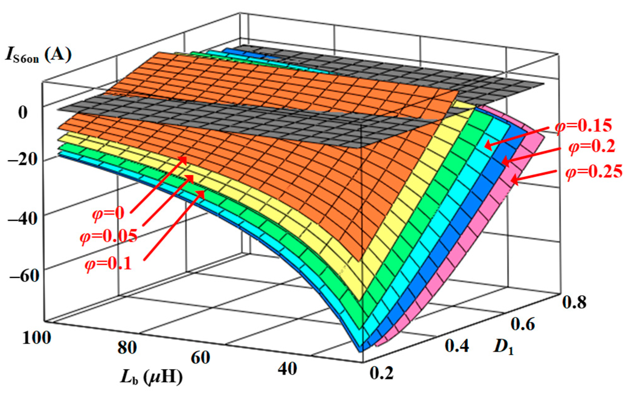
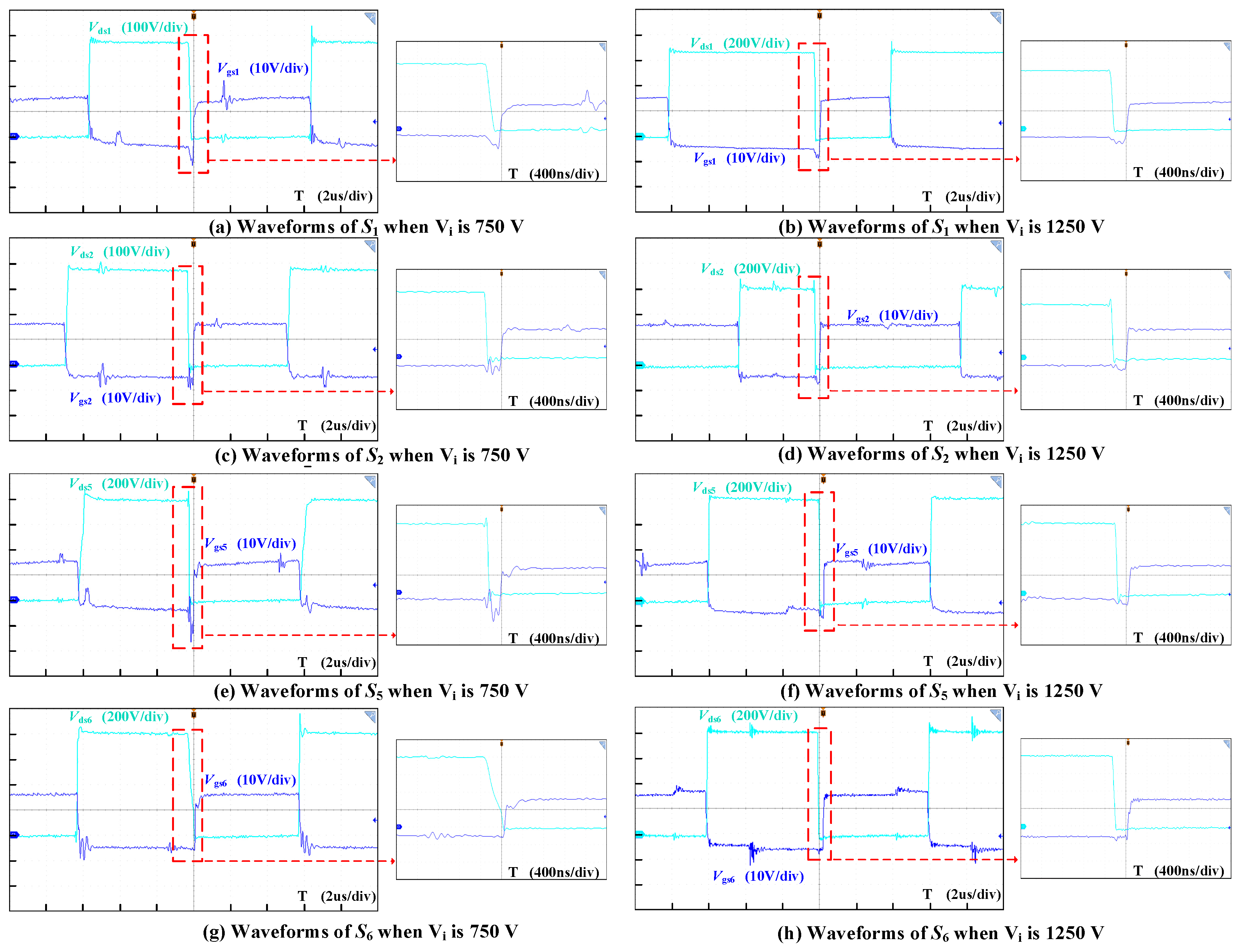
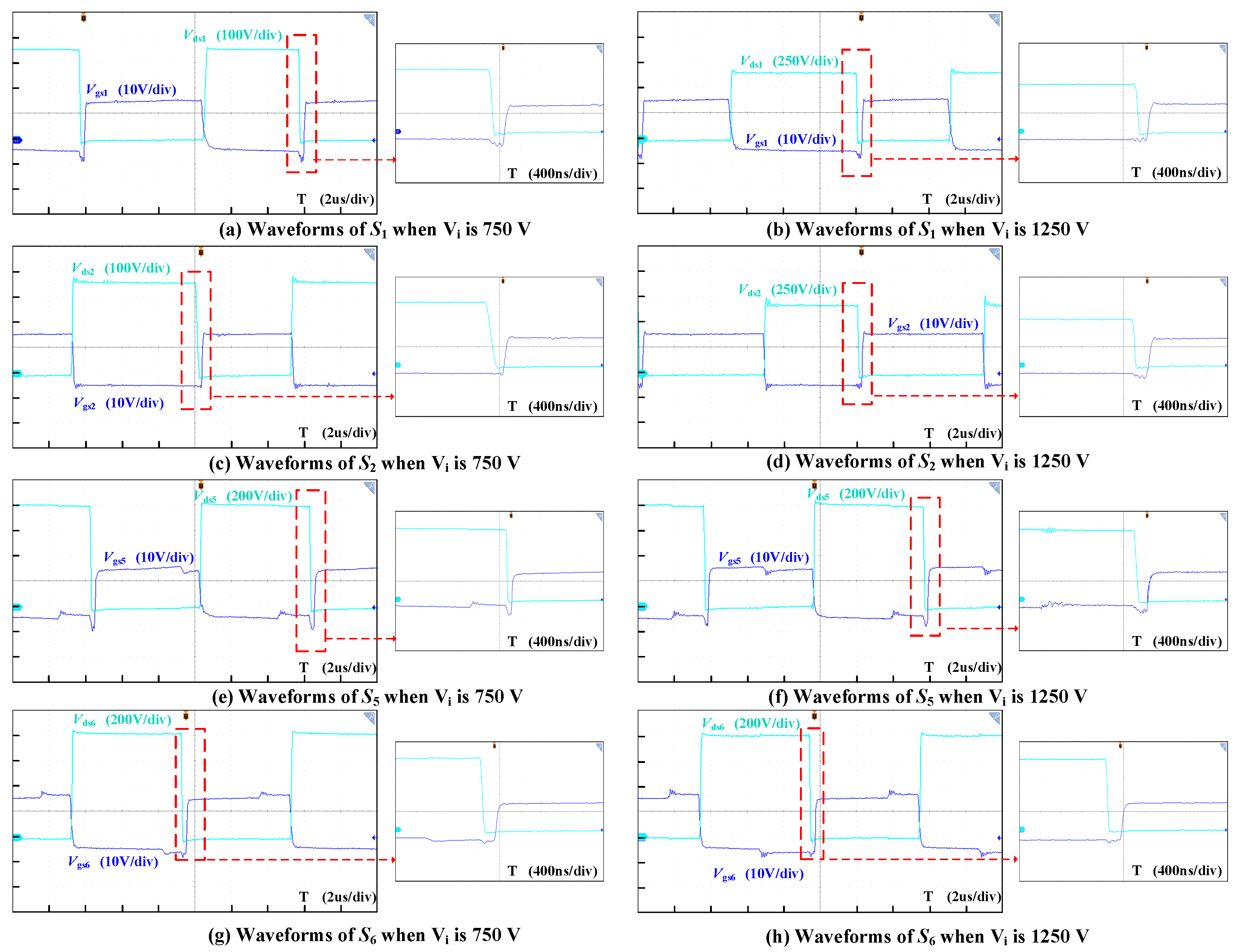
3.4. Soft-Switching Characteristics

Through modal analysis, it can be found that the ZVS realization of switching tube S1~S4 is mainly determined by inductor current ILb, ILa1, and ILa2. The ZVS realization of switching tube S5~S6 is mainly determined by inductor current ILb and resonant current ILr. Taking mode X1 as an example, the switching tubes S2 and S3 are off at t4′ time. Before the switching tube S4 and S1’s driving signal rises, the auxiliary inductors La1 and La2 will provide a reverse bias current. The junction capacitance of the switching tube S4 and S1 gradually begins to discharge, and the drain-source voltage Vds1 and Vds4 rapidly drops to 0. From that point, the driving signal of the switching tubes S1 and S4 begins to rise, and S1 and S4 realize ZVS. For the switching tube S2 and S3, the switching tubes S1 and S4 are off at t2 time. Before the switching tube S2 and S3’s driving signal rises, the inductors La1, La2, and Lb provide reverse currents. The junction capacitance of the switching tube S2 and S3 gradually begins to discharge, and the drain-to-source voltage Vds2 and Vds3 rapidly drops to 0. From that point, the driving signal of the switching tube S2 and S3 begins to rise, and S2 and S3 realize ZVS. For the switching tube S5, the switching tube S6 is off at t1′, and before the drive signal of S5 rises, the buck inductor Lb will provide a reverse current for S5. The junction capacitance of S5 gradually discharges, and the drain-to-source voltage Vds5 rapidly drops to 0. After that, the drive signal of S5 begins to rise, and S5 realizes ZVS. For the switching tube S6, the switching tube S5 is off at t3, and before the driving signal of the switching tube S6 rises, the reverse current comes from the resonant inductor Lr. The junction capacitance of the switching tube S6 gradually begins to discharge, and the drain-to-source voltage Vds6 rapidly drops to 0. After that, the driving signal of the switching tube S6 begins to rise, and S6 realizes ZVS. It is defined that the complete charge and discharge current of the junction capacitor is ΔIZVS. To ensure that the junction capacitor can discharge to 0 to meet ZVS in each switching dead time, the instantaneous current value of the switching tubes at the opening time must be less than −ΔIZVS.
Therefore, the ZVS condition of each switching tube in the power unit can be expressed by the following equation:
I S 1 - on = I S 4 - on = I Lb ( t 0 ) I La 1 ( t 0 ) Δ I ZVS
I S 2 - on = I S 3 - on = I La 1 ( t 2 ) I Lb ( t 2 ) Δ I ZVS
I S 5 - on = I Lr ( t 1 ) I Lb ( t 1 ) Δ I ZVS
I S 6 - on = I Lb ( t 3 ) I Lr ( t 3 ) Δ I ZVS
By extension of the power expression mentioned above, Equation (23) can be obtained.
I p = 2 P X 1 Y 2 V Cc V Cc 2 T s 2 L b V Cc ( φ 2 D 1 + 2 φ D 1 + 0.5 )
Then, Equation (24) can be obtained:
I Lb ( t 3 ) = I Lb ( t 0 ) = I p
According to the above analysis, when the converter is in the half-load or no-load state, its ZVS condition is easier to achieve than the full-load state. Therefore, the following analysis only considers the ZVS condition of the converter at full load. ILa1(t2′) and ILb(t2′) are constant negative and positive values, respectively, so the inherent characteristics of S3 and S2 meet the ZVS condition in a wide operating range. The ZVS conditions of S1, S4, S5, and S6 need to be analyzed according to specific working conditions.
The Fourier expansion expression of the input voltage VCB of the resonator is shown as follows:
V CB = ( 1 D 2 ) V Cc + V sh
V s h = h = 1 2 V Cc h π 1 cos ( 2 h π D 2 ) sin ( 2 h π f s t + θ h )
Among them,
θ h = tan 1 ( sin ( 2 h π D 2 ) 1 cos ( 2 h π D 2 ) ) = π 2 h D 2 π
According to the resonator transfer function shown in Equation (10), the expressions of excitation inductance current ILm and equivalent load current Ioe in the steady-state equivalent circuit shown in Figure 8 can be easily derived.
I Lm = n h = 1 H h V CBh j h ω L m
I oe = n h = 1 H h V CBh R e q
The resonant current ILr can be obtained by adding the above two formulas.
I L r ( t ) = h = 1 2 V Cc h π 1 cos ( 2 h π D 2 ) { | n T H h | R e q sin ( 2 h π f s t + θ h + ( n T H h ) ) | n T H h | h ω L m cos ( 2 h π f s t + θ h + ( n T H h ) ) }
When fs = 80 k, P = 6.25 kW, and Vo = 400 V, the relationship between the opening current IS5on of S5 and IS6on of S6, duty cycle D1, phase shift φTs, and buck inductance Lb can be obtained by combining the inductance expression (16) derived above, as shown in Figure 10 and Figure 11, respectively. Considering the transmission power and voltage level comprehensively, the value of ΔIZVS is 1.5 A, and the dark-colored plane in the figure is the reference plane of Ion = −1.5 A. It can be found that the ZVS range of S6 and S5 is relatively wide. When φ is less than 0.1, ZVS of S5 cannot be realized under the condition of a low-duty cycle. The increase in inductance Lb causes the opening current of S5 to increase. When the duty cycle of S6 is more significant than 0.3, there are working points where S6 cannot realize ZVS. But with the increase of phase shift φTs or the decrease of inductance Lb, the working range meeting the ZVS condition will gradually expand.
According to the volt-second balance of La1, namely (1 − D1)TsVc2 = D1TsVc1, and the symmetry of the series-type double-buck circuit (Vc1 + Vc2 = Vc3 + Vc4 = Vi/2), it can be calculated:
V c 1 = ( 1 D 1 ) V i / 2
V c 2 = D 1 V i / 2
The peak value of the auxiliary inductance current can be calculated by the following equation:
| i L a 1 p k + | = | i L a 1 p k | = 1 L a 1 D 1 T s / 2 V c 1 d t = D 1 ( 1 D 1 ) 4 f s L a 1 V i
I S 1 - on = I S 4 - on = I p D 1 ( 1 D 1 ) 4 f s L a 1 V i
When fs = 80 k, P = 6.25 kW, Vo = 400 V, and Lb = 75 μH, the relationship between the opening current IS1on and IS4on of S1 and S4, duty cycle D1, phase shift φTs, and auxiliary inductance La1 can be obtained, as shown in Figure 12. The gray plane in the figure is the reference plane of Ion = −1.5 A. The increase in phase shift φTs reduces the ZVS difficulty of S1 and S4; the decrease of auxiliary inductance La1 increases the negative bias current when the switching tube is opened, making ZVS easier to realize. At the same time, the introduced bias current will lead to a slight increase in the conduction loss. From this point of view, the value of the auxiliary inductance La1 should not be too small.

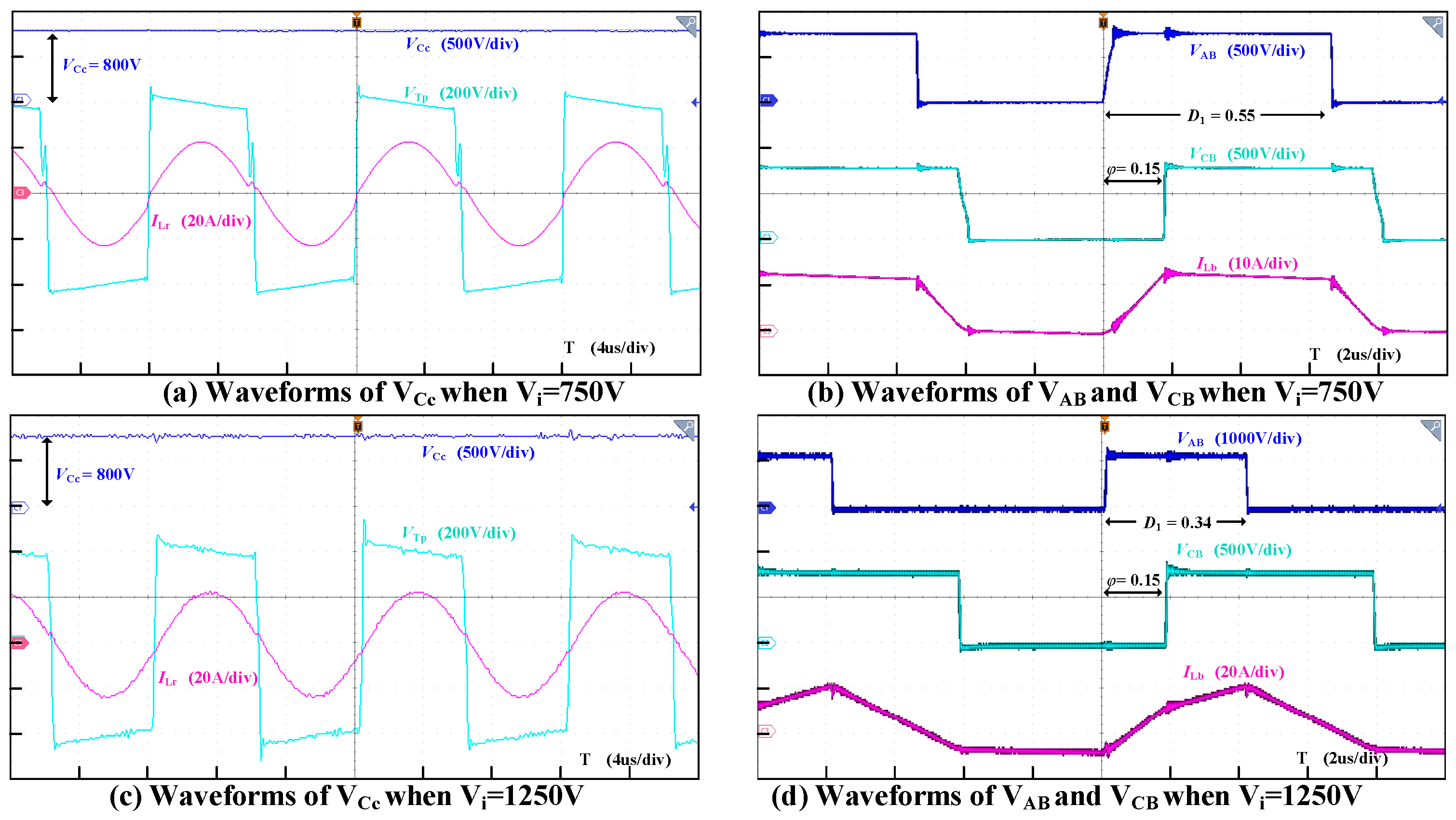
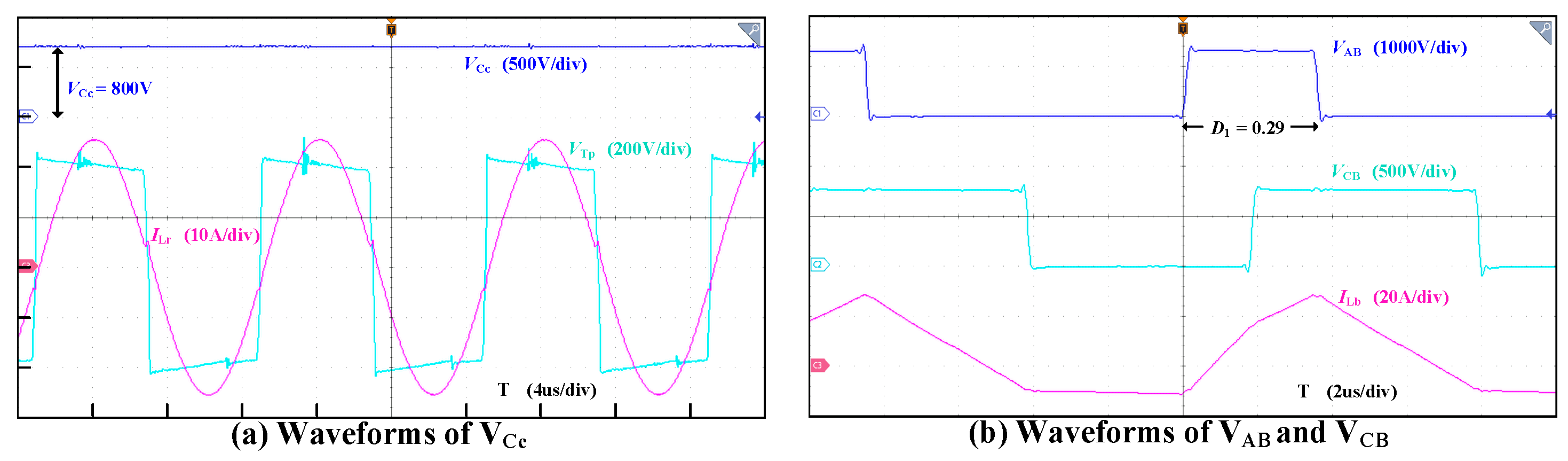
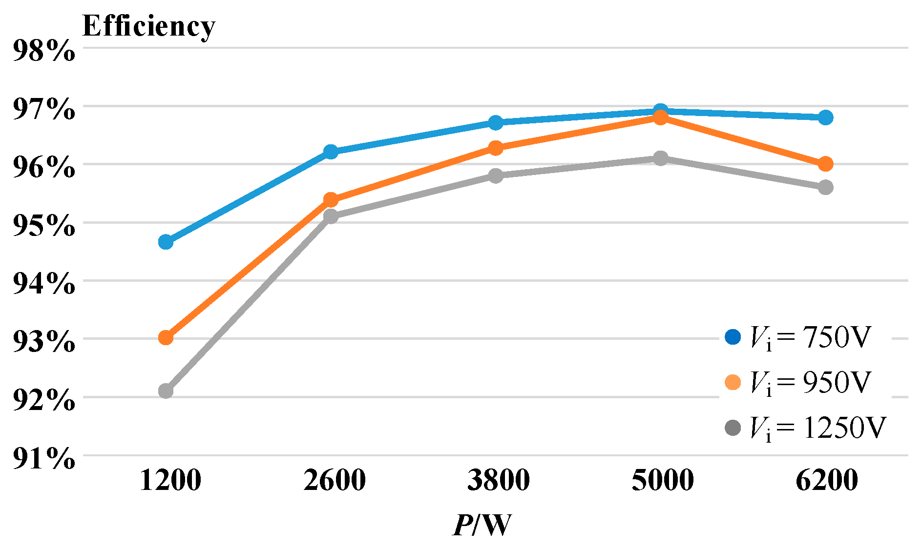
4. Experimental Verification

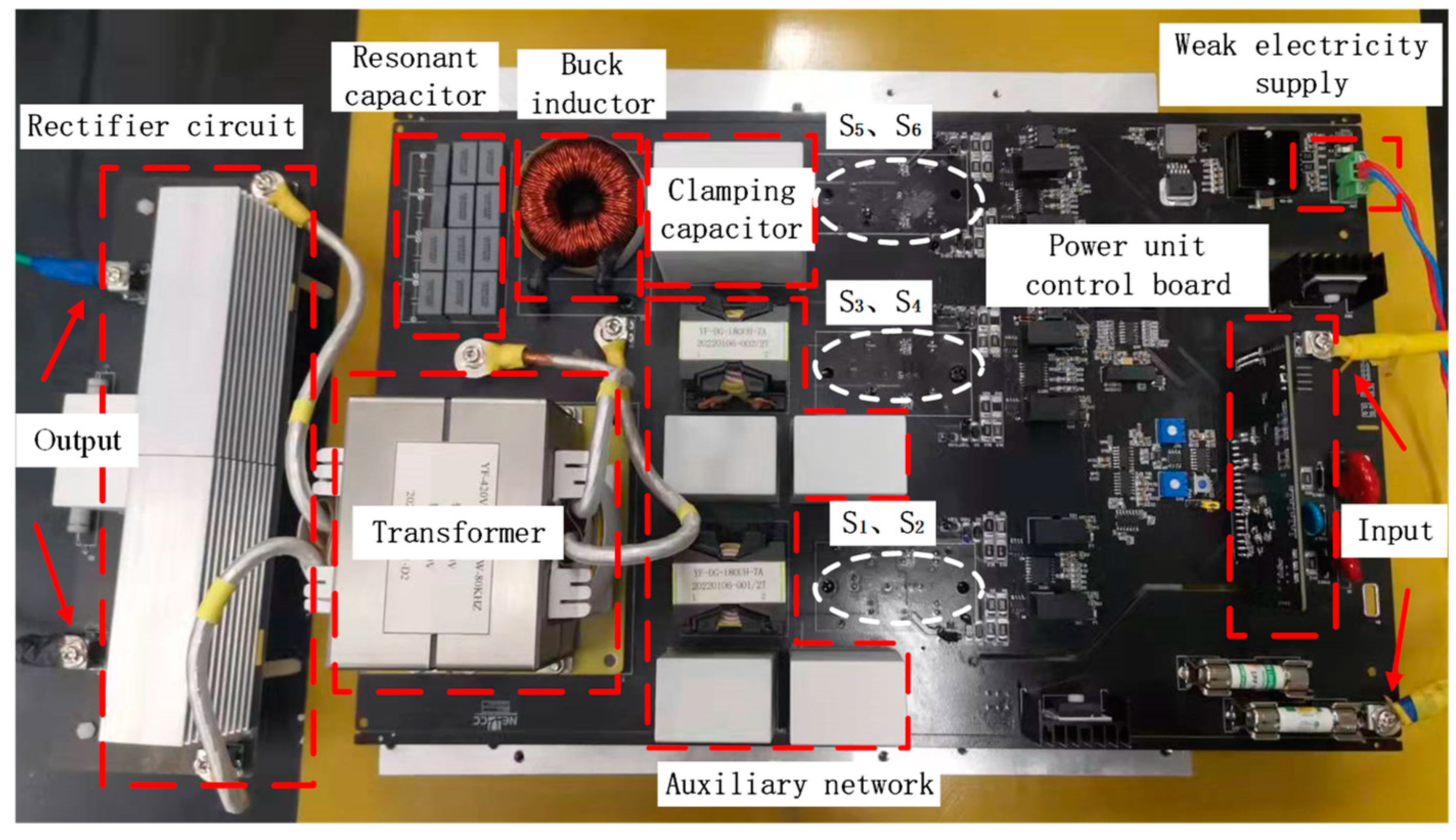
4.1. Experimental Prototype

An experimental prototype of 6.25~7 kW was designed and developed to prove the feasibility of the proposed power unit topology and the correctness of the above analysis. It meets the requirements of a wide input voltage range of 750 V~1430 V. Table 3 shows the device parameters of the experimental prototype, and Figure 13 shows the experimental prototype.

4.2. Experimental Scheme

The DC converter engineering prototype meets the needs of 6–10 kV medium-voltage DC power grid access, including eight power units, with one power unit redundancy switching capability. When eight power units operate, the input voltage range of a single power unit is 750~1250 V, the output voltage is 400 V, and the output power is 6.25 kW. When seven power units operate, the input voltage range of a single power unit is 860~1430 V, and the output power is 7.15 kW.
Figure 14 shows the steady-state experimental waveforms under different input voltages and rated power conditions when eight power units work. VTp is the input voltage on the primary side of the transformer. Figure 14a,b corresponds to the steady-state waveforms when the input voltage of the power unit is 750 V and D1 = 0.55. The power unit works in mode Y2. As shown in the figure, the amplitude of VAB is equal to the input voltage, which is 750 V. The amplitude of VCB, the input voltage of the resonator, is equal to the clamp capacitor voltage VCc, which is 800 V. Under D2 = 0.5 and nT = 1, the output voltage is stable at 400 V. Currently, the current offset provided by the auxiliary network is the lowest, and it is the most difficult with which to realize ZVS. Figure 14c,d corresponds to the steady-state waveforms when the input voltage of the power unit is 1250 V, D1 = 0.34, and mode X1. As shown in the figure, the VAB amplitude equals the input voltage, which is 1250 V. VCB amplitude, namely the input voltage of the resonator, is equal to the clamp capacitor voltage VCc, which is still 800 V. In these two operating modes, each electrical parameters of the LLC resonator are the same. Figure 15 shows the steady-state experimental waveforms when the input voltage of the power unit is 1400 V when seven power units operate. The output power is 7 kW, D1 = 0.29, and the power unit works in mode X1. As shown in the figure, the VAB amplitude equals the input voltage, which is 1400 V. The VCB amplitude is equal to the clamp capacitor voltage VCc, which is still 800 V.
Figure 16 shows the ZVS waveforms of each switching tube at different input voltages under full load conditions. Due to the symmetric relationship between S1 and S4, and S2, and S3, only related waveforms of S1 and S2 are shown in this paper. Figure 16a,c,e,g respectively shows the drain-source voltage and gate-source voltage waveforms of S1, S2, S5, and S6 when the input voltage is 750 V under full-load conditions. It can be seen that S1 and S6 are in the most difficult ZVS condition in the whole working range. The time difference between the falling edge of drain-source voltage and the rising edge of gate-source voltage of S1 is less than 100 ns. The time difference between the falling edge of drain-source voltage and the rising edge of gate-source voltage of S6 is only 20 ns. Figure 16b,d,f,h respectively show the drain-source voltage and gate-source voltage waveforms of S1, S2, S5, and S6 when the input voltage is 1250 V under full-load conditions. The time difference between the drain-source voltage falling edge and the gate-source voltage rising edge of each switching tube is more incredible than 160 ns, which can quickly achieve ZVS.
Figure 17 shows the ZVS waveforms of each switching tube at different input voltages under a 20% load condition (1200 W). Figure 17a,c,e,g respectively corresponds to the ZVS waveforms of S1, S2, S5, and S6 when the input voltage is 750 V. Figure 17b,d,f,h respectively corresponds to the ZVS waveforms of S1, S2, S5, and S6 when the input voltage is 1250 V. It can be seen that under light load conditions, there is a long-time difference between the drain-source voltage falling edge and the gate-source voltage rising edge. Thus, ZVS can be easily realized. In summary, ZVS can be realized in a wide input voltage and output power range for all switching tubes for the proposed SDBuck-LLC resonant converter. Figure 18 shows the efficiency comparison of the power unit under different input voltages. The variation curves of converter efficiency with output power are shown under input voltage 750 V, 950 V, and 1250 V, respectively. The power of each operating point is measured by the power analyzer HIOKI-PW6001. As seen in Figure 18, the efficiency of the power unit decreases slightly with the increase in the input voltage. Still, the efficiency under full-load conditions is higher than 95% in a wide input voltage range.

5. Conclusions

A DC transformer is an efficient power electronic equipment with DC voltage conversion and DC energy distribution abilities, which is the key technology for the development and construction of a DC power grid. This paper studied the DC converter for renewable energy access, and a Buck-LLC integrated modular combined DC converter was proposed. Great breakthroughs were made in theoretical research and engineering prototype development. The topology can meet the requirements of a wide voltage range on the medium voltage side. The converter takes SDBuck-LLC as its power unit, which consists of an auxiliary network, series buck, integrated LLC resonant circuit, isolation transformer, and rectifier circuit. The circuit structure adopts an integrated design and has a high-power density. The duty cycle of a series double-buck circuit can be adjusted to suit the application of a wide input voltage range. Through the auxiliary circuit and the phase shift φTs introduced, all the switching tubes can realize ZVS in a wide input voltage range. Thus, the turn-on loss is eliminated, and the overall conversion efficiency of the converter is improved. The experimental prototype of the power unit was designed, the experimental results of the prototype were shown, and the feasibility of the proposed power unit was verified. The work in this paper is helpful for subsequent research on DC converters, such as the analysis of the electromagnetic energy interaction mechanism inside the DC converter, the construction of a complete and accurate loss model of the DC converter, and the exploration of the core factors affecting the operation efficiency of the DC converter. Therefore, this work lays a foundation for proposing a globally oriented theory and method for the optimization of the operation efficiency of the DC converter.

Author Contributions

Conceptualization, D.W. and Q.Z.; methodology, D.W.; software, D.W.; validation, D.W., X.D. and J.Z.; formal analysis, J.L.; investigation, D.W.; resources, D.W.; data curation, D.W.; writing—original draft preparation, D.W.; writing—review and editing, D.W.; visualization, J.L.; supervision, H.Z.; project administration, D.W.; funding acquisition, D.W. All authors have read and agreed to the published version of the manuscript.

Funding

The author(s) declare financial support was received for the research, authorship, and/or publication of this article. This work is supported by State Grid Hunan Electric Power Company Science and Technology Project “Technology and Demonstration of Distributed Flexible Resource Cluster Autonomy and Provincial Local-County Collaborative Dispatch in Active Distribution Networks” (5216A522000M).

Data Availability Statement

No new data were created or analyzed in this study. Data sharing is not applicable to this article.

Conflicts of Interest

The authors declare no conflict of interest.

References

  1. Rong, Z.; Zhao, Y.; Zhao, B.; Qing, Z.; Tong, Y.; Yuan, Z.; Yu, Z.; Zhao, Z.; Li, Y.; Chen, J. A Prospective Look on Research and Application of DC Power Distribution Technology. Proc. CSEE 2018, 38, 6791–6801, 7114. [Google Scholar]
  2. Han, Y.; Gao, Y.; Zheng, W.; Zhang, J.; Zhang, J.; Li, L. Study on coordination protection of overcurrent and overvoltage in multiterminal VSC-DC distribution system. South. Power Syst. Technol. 2019, 13, 1–8. [Google Scholar]
  3. Gomis-bellmunt, O.; Sau-Bassols, J.; Prieto-Araujo, E. Flexible converters for meshed HVDC grids: From flexible AC transmission systems (FACTS) to flexible DC grids. IEEE Trans. Power Deliv. 2020, 35, 2–15. [Google Scholar] [CrossRef]
  4. Shuai, Z.; Huang, W.; Shen, C.; Ge, J.; Shen, Z.J. Characteristics and restraining method of fast transient inrush fault currents in synchronverters. IEEE Trans. Ind. Electron. 2017, 35, 7487–7497. [Google Scholar] [CrossRef]
  5. Liu, B.; Tu, C.; Xiao, F.; Yu, X.; Guo, Q.; Shuai, Z. Overview of Topology and Control of Medium and Low Voltage DC Transformers. Electr. Power Autom. Equip. 2021, 41, 232–246. [Google Scholar]
  6. Nabae, A.; Takahashi, I.; Akagi, H. A new neutral-point-clamped PWM inverter. IEEE Trans. Ind. Appl. 1981, IA–17, 518–523. [Google Scholar] [CrossRef]
  7. Montesinos-Miracle, D.; Massot-Campos, M.; Bergas-Jane, J.; Galceran-Arellano, S.; Rufer, A. Design and control of a modular multilevel DC/DC converter for regenerative applications. IEEE Trans. Power Electron. 2013, 28, 3970–3979. [Google Scholar] [CrossRef]
  8. Zhao, X.; Li, B.; Fu, Q.; Mao, S.; Xu, D.; Leon, J.I.; Franquelo, L.G. DC solid state transformer based on three-level power module for interconnecting MV and LV DC distribution systems. IEEE Trans. Power Electron. 2021, 36, 1563–1577. [Google Scholar] [CrossRef]
  9. Quraan, M.; Yeo, T.; Tricoli, P. Design and control of modular multilevel converters for battery electric vehicles. IEEE Trans. Power Electron. 2016, 31, 507–517. [Google Scholar] [CrossRef]
  10. Yang, J.; Zhang, K.; Chen, W.; Zhao, G.; Chen, Z.; Dong, K. Review on researches of high-power medium-frequency transformer. J. Power Supply 2020, 18, 4–17. [Google Scholar]
  11. Sun, C.; Zhang, J.; Cai, X.; Shi, G. Analysis and arm voltage control of isolated modular multilevel DC-DC converter with asymmetric branch impedance. IEEE Trans. Power Electron. 2016, 32, 5978–5990. [Google Scholar] [CrossRef]
  12. Chen, Y.; Zhao, S.; Li, Z.; Wei, X.; Kang, Y. Modeling and control of the isolated DC–DC modular multilevel converter for electric ship medium voltage direct current power system. IEEE J. Emerg. Sel. Top. Power Electron. 2017, 5, 124–139. [Google Scholar] [CrossRef]
  13. Zhao, B.; Song, Q.; Li, J.; Wang, Y.; Liu, W. High-Frequency-Link Modulation Methodology of DC-DC transformer based on modular multilevel converter for HVDC application: Comprehensive Analysis and Experimental Verification. IEEE Trans. Power Electron. 2017, 32, 3413–3424. [Google Scholar] [CrossRef]
  14. Yu, F.; Wang, Z.; Liu, X. A gradationally controlled modular multilevel converter and its application. Power Syst. Prot. Control 2022, 50, 69–77. [Google Scholar]
  15. Cui, S.; Soltau, N.; De Doncker, R.W. A high step-up ratio soft-switching DC–DC converter for interconnection of MVDC and HVDC Grids. IEEE Trans. Power Electron. 2018, 33, 2986–3001. [Google Scholar] [CrossRef]
  16. Xiang, X.; Zhang, X.; Luth, T.; Merlin, M.M.; Green, T.C. A compact modular multilevel DC–DC converter for high step-ratio MV and HV use. IEEE Trans. Ind. Electron. 2018, 65, 7060–7071. [Google Scholar] [CrossRef]
  17. Shi, Y.; Mo, R.; Li, H.; Pan, Z. A novel ISOP current-fed modular dual-active-bridge (CF-MDAB) DC-DC converter with DC fault ride-through capability for MVDC application. In Proceedings of the 2017 IEEE Energy Conversion Congress and Exposition, Cincinnati, OH, USA, 1–5 October 2017. [Google Scholar]
  18. Shi, Y.; Li, H. Isolated Modular multilevel DC–DC converter with DC fault current control capability based on current-fed dual active bridge for MVDC application. IEEE Trans. Power Electron. 2018, 33, 2145–2161. [Google Scholar] [CrossRef]
  19. Jovcic, D. Bidirectional, High-power DC transformer. IEEE Trans. Power Deliv. 2009, 24, 2276–2283. [Google Scholar] [CrossRef]
  20. Zhang, X.; Green, T.C.; Junyent-Ferre, A. A new resonant modular multilevel step-down DC–DC converter with inherent-balancing. IEEE Trans. Power Electron. 2015, 30, 78–88. [Google Scholar] [CrossRef]
  21. Xiang, X.; Zhang, X.; Chaffey, G.P.; Green, T.C. An isolated resonant mode modular converter with flexible modulation and variety of configurations for MVDC application. IEEE Trans. Power Deliv. 2018, 33, 508–519. [Google Scholar] [CrossRef]
  22. Chen, W. Research on Series and Parallel Combination System of Multi-Converter Module; Nanjing University of Aeronautics and Astronaut: Nanjing, China, 2009. [Google Scholar]
  23. Zhao, B.; Song, Q.; Liu, W.; Sun, Y. Overview of dual-active-bridge isolated bidirectional DC–DC converter for high-frequency-link power-conversion system. IEEE Trans. Power Electron. 2014, 29, 4091–4106. [Google Scholar] [CrossRef]
  24. Zhao, B.; Song, Q.; Liu, W. High-frequency-link DC solid state transformers for flexible dc distribution. Proc. CSEE 2014, 34, 4295–4303. [Google Scholar]
  25. Chub, A.; Costa, L.; Liserre, M. Analysis and design of asymmetric quad-active-bridge converter. In Proceedings of the IECON 2017—43rd Annual Conference of the IEEE Industrial Electronics Society, Beijing, China, 29 October–1 November 2017. [Google Scholar]
  26. Ji, Z. Research on Key Techniques of Cascaded Power Electronic Transformer; Southeast University: Nanjing, China, 2015. [Google Scholar]
  27. Costa, L.F.; De Carne, G.; Buticchi, G.; Liserre, M. The smart transformer: A solid-state transformer tailored to provide ancillary services to the distribution grid. IEEE Power Electron. Mag. 2017, 4, 56–67. [Google Scholar] [CrossRef]
  28. Huber, J.E.; Kolar, J.W. Applicability of solid-state transformers in today’s and future distribution grids. IEEE Trans. Smart Grid 2019, 10, 317–326. [Google Scholar] [CrossRef]
Figure 1. Modular combined DC-DC converter based on Buck-LLC integration.
Electronics 12 03975 g001
Figure 2. Waveforms of each operational mode of SDBuck-LLC.
Electronics 12 03975 g002
Figure 3. Key voltage and current waveforms of SDBuck-LLC (a) mode X1 and (b) mode Y2.
Electronics 12 03975 g003
Figure 4. Equivalent circuits of stage 1 and stage 2 in mode X1.
Electronics 12 03975 g004
Figure 5. Equivalent circuits of stage 3 and stage 4 in mode X1.
Electronics 12 03975 g005
Figure 6. Equivalent circuits of stage 5 and stage 6 in mode X1.
Electronics 12 03975 g006
Figure 7. Equivalent circuits of stage 7, stage 8, and stage 9 in mode X1.
Electronics 12 03975 g007aElectronics 12 03975 g007b
Figure 8. Steady-state equivalent circuit of SDBuck-LLC.
Electronics 12 03975 g008
Figure 9. The relationship between power P and D1, Lb under different phase shifts φTs.
Electronics 12 03975 g009
Figure 10. The relationship between IS5on and D1, Lb under different phase shifts φTs.
Electronics 12 03975 g010
Figure 11. The relationship between IS6on and D1, Lb under different phase shifts φTs.
Electronics 12 03975 g011
Figure 12. The relationship between IS1on, IS4on, and D1, Lb under different phase shifts φTs.
Electronics 12 03975 g012
Figure 13. Experimental prototype of SDBuck-LLC.
Electronics 12 03975 g013
Figure 14. Steady-state experimental waveform of SDBuck-LLC with an output power of 6.25 kW under different Vi.
Electronics 12 03975 g014
Figure 15. Steady-state experimental waveforms of SDBuck-LLC with an output power of 6.25 kW and input voltage of 1400 V.
Electronics 12 03975 g015
Figure 16. ZVS waveforms of each switch under full load and different input voltages Vi.
Electronics 12 03975 g016
Figure 17. ZVS waveforms of each switch under light load and different input voltages Vi.
Electronics 12 03975 g017
Figure 18. Efficiency curves of SDBuck-LLC under different input voltages Vi.
Electronics 12 03975 g018
Table 1. Comparisons among different DC converters in references.
Refs.Voltage StressZVS AbilityTracking
Performance
[9]MediumPoorPoor
[13]LowMediumGood
[20]HighMediumMedium
[25]LowMediumGood
ProposedLowGoodGood
Table 2. Submodule SDBuck-LLC operational mode division.
Mode1234
X (0 < D1 ≤ 0.5)0 < φD1D1 < φ ≤ 0.50.5 < φD1 + 0.5D1 + 0.5 < φ ≤ 1
Y (0.5 < D1 ≤ 1)0 < φD1–0.5D1–0.5 < φ ≤ 0.50.5 < φD1D1 < φ ≤ 1
Table 3. Experimental prototype parameters.
ParametersValuesParametersValues
Input voltage (Vi)750 V~1430 VRated output power (Po*)6.25~7 kW
Output voltage (Vo)400 VRated switching frequency (fsn)80 kHz
Resonant inductor (Lr)14.3 μHTransformer turns ratio (nT)1:1
Input capacitance (C1~C4)50 μFAuxiliary inductors (La1, La2)180 μH
Phase shift (φ)0.15Resonant inductor (Lb)75 μH
Clamp capacitor (Cc)55 μFResonant capacitance (Cr)276.6 nF
Disclaimer/Publisher’s Note: The statements, opinions and data contained in all publications are solely those of the individual author(s) and contributor(s) and not of MDPI and/or the editor(s). MDPI and/or the editor(s) disclaim responsibility for any injury to people or property resulting from any ideas, methods, instructions or products referred to in the content.

