Communication

Design of a Clock Doubler Based on Delay-Locked Loop in a 55 nm RF CMOS Process

1
Department of Electrical and Computer Engineering, Sungkyunkwan University, Suwon 16419, Republic of Korea
2
SKAIChips, Suwon 16419, Republic of Korea
*
Author to whom correspondence should be addressed.
Electronics 2023, 12(13), 2830; https://doi.org/10.3390/electronics12132830
Submission received: 15 May 2023 / Revised: 10 June 2023 / Accepted: 25 June 2023 / Published: 26 June 2023
(This article belongs to the Special Issue Advances in RF, Analog, and Mixed Signal Circuits)

Abstract

:
In this paper, for the wireless network, wearable device, and Internet of Things (IoT) markets, a delay-locked loop (DLL) is used to implement accurate multiplication for a reference clock and the frequency of various applications through an edge combiner (EC). A simpler structure is more sensitive to process, voltage, and temperature (PVT), so DLL complements itself quickly in the feedback system and improves the stability of the final output. The proposed DLL-based multiplier can prevent harmonic lock generation using a first phase canceller (FPC), thus compensating for faster lock time. The circuit is built with a 55 nm CMOS process and has a chip area of 0.0225 mm2. The proposed design achieves a total power consumption of 0.48 mW at the 30.72 MHz operating clock frequency, and the clock duty can also operate stably from 15 to 75%.

1. Introduction

Recently, the wireless network industry has rapidly evolved, leading to an increased demand for more efficient communication methods and high-performance microprocessors necessary to handle the vast quantities of data transmitted across these networks. This has resulted in a significant surge in demand for such devices in the market. Multipliers are often used at frequencies ranging from several GHz or higher. The frequency should be very stable, but the frequency gets higher, it becomes increasingly challenging to design a structure that effectively stabilizes the frequency.
In today’s advanced technologies, it is crucial for integrated circuits (ICs) to generate high-speed clock signals from low-speed external sources such as crystal oscillators. Clock doublers have become increasingly prevalent in integrated circuits. In use, they can be incorporated at the input of a phase-locked loop (PLL) and utilized with UARTs to achieve greater bandwidth, while also serving as a valuable component in a clock distribution network [1,2]. To achieve this, on-chip clock multiplication has become essential. One common approach for clock multiplication is to use a phase-locked loop (PLL) circuit. A PLL typically consists of a phase detector, an analog loop filter, a divider, and a voltage-controlled oscillator (VCO) [3]. However, PLLs have a significant analog content, which can make their design challenging to fit into a typical digital design flow. The analog components of the PLL, including the loop filter and VCO, require careful consideration of noise, stability, and other factors that are typically not necessary in digital circuits. This can make the design process more complex and time-consuming, especially for digital designers who may not have a strong background in analog circuit design.
Despite these challenges, PLLs remain a popular choice for clock multiplication due to their versatility and ability to generate stable, high-quality clock signals. As a result, efforts have been made to simplify the design of PLLs and reduce their analog content, such as through the use of digital loop filters and all-digital PLLs. These approaches can help to reduce the design complexity of PLLs and make them more accessible to digital designers. So, by creating a stabilized frequency source at a low frequency and increasing it to an accurate magnification through the harmonic calculation of the multiplier, it is often possible to secure a frequency source for the LO, etc., required for ultra-high frequency communication. When designing wearable devices or Internet of Things (IoT) devices, the reference clock signal is a critical component. It is essential to generate stable and accurate clock signals that can meet the requirements of the intended application. One common approach to generating a high-speed clock signal is to use a frequency multiplier circuit.
The conventional structure used for frequency multiplication typically employs an XOR gate. The structure must be designed to operate at the desired supply voltage while providing the required clock speed for the intended application. However, designing an efficient frequency multiplier circuit can be challenging due to factors such as power consumption, noise, and layout restrictions. For wearable and IoT devices, power consumption is a crucial consideration, and the frequency multiplier circuit must be designed to operate at low power levels to extend battery life. In addition, the small form factor of these devices means that the layout of the frequency multiplier circuit must be carefully optimized to reduce the size of the overall system.
Frequency multiplier circuits are essential components of many wearable and IoT devices. The development of more efficient and compact frequency multiplier circuits has enabled the creation of new generations of wearable and IoT devices with advanced capabilities, such as low-power wireless connectivity, sensor fusion, and machine learning.
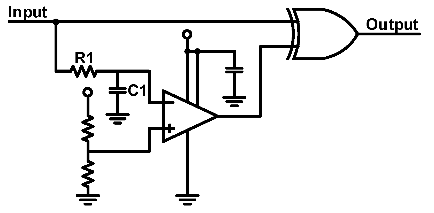
The input frequency of the above circuit, Figure 1, operates as an input of the XOR gate and an input of the configured delay circuit. The delay circuit consisting of a resistor (R1), a capacitor (C1), and a comparator shown in the figure above provides the second input of the XOR gate. Additionally, the other input to the comparator is supply voltage, which is 50% of the reference voltage through resistance distribution. The above figure’s values, R1 and C1, are derived from the equation:
R 1 C 1 = 2 3 1 f D O U B L E
Here, f D O U B L E represents the desired frequency output which is twice the original frequency. However, it is difficult to obtain a frequency that multiples the input frequency depending on temperature and process by reacting insensitively to PVT, or to operate normally with a constant pulse of 50% duty.
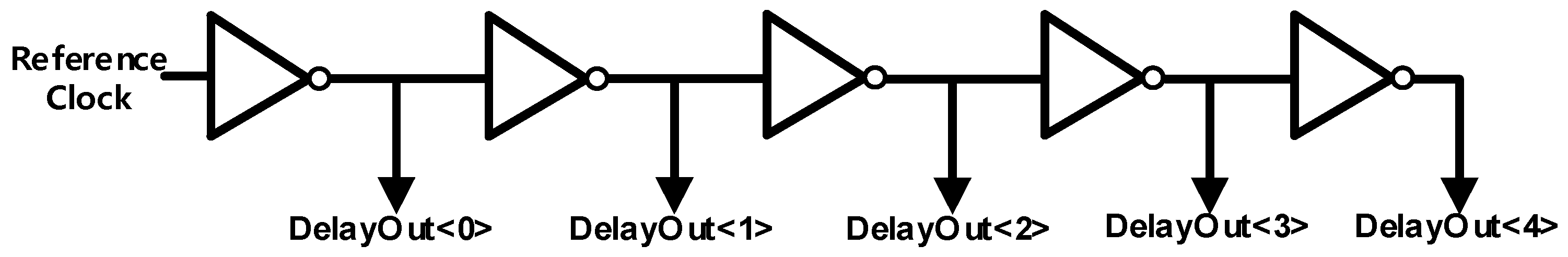
Figure 2 is proposed DLL Top block diagram. The proposed approach to prevent harmonic locking and ensure optimal performance within a defined frequency range is accomplished by employing a delay-locked loop (DLL) that is constructed with the help of several components, namely: a phase frequency detector (PFD), charge pump (CP), and a loop filter (LF) based on the voltage-controlled delay line (VCDL). Additionally, the first phase canceller (FPC) is an essential part of this structure. It satisfies the requirements of a system that generates clock frequencies with multiple phase sampling methods, and also meets the requirements for operating frequency in low-frequency or high-frequency systems synchronized with peripheral devices.

2. MDLL Architecture

2.1. MDLL Top Block Diagram

Figure 3 is the top block diagram of the multiplying delay-locked loop. First, for two input signals, harmonic lock is prevented from being generated through FPC, and a signal is sent to detect the phase and frequency difference in the analog PFD, and the up signal and down signal are transmitted to the CP with a clock pulse. The current of the CP is adjusted according to the up/down signal, which is transmitted to the VCDL through LF. The VCDL, which operates based on the reference clock, detects the change in input voltage and changes the pulse interval for each delay line, aiming at aligning the reference signal and the final signal. The delay signals except for the feedback signal, are then sent to the edge combiner, and the frequency is multiplied through the internal multiplexer and D-flip flop.

2.2. Voltage Controlled Delay Line

Figure 4 shows the VCDL’s schematic, which uses a current-starved inverter and shunt capacitor to generate signal delay. The alignment of the first and last signals is used to synchronize the DLL initial signal and the edge combiner. However, increasing the number of delay cells or size of internal elements to achieve a higher frequency range can introduce more phase noise and necessitate additional circuits for compensation.
Figure 5 shows the normal operation of the VCDL. The signals used for the DLL locking with Delay Out<4> and Delay Out<0> are the final outputs of the VCDL. It is designed to have a difference of one cycle of the reference clock. Initially, the circuit has arbitrary signals, but as the DLL progresses, it creates a one-cycle difference as shown in the figure. However, this process is at risk of harmonic locking, a frequent problem in DLLs that hampers the exact one-cycle difference. In the next part, it will be explained how the first phase canceller can prevent this problem. The red arrows are the rising edges of the delay pulses that are shown synchronized by the gray dashed lines.

2.3. First Phase Canceller

Figure 6 shows the schematic of the first phase canceller, which is used to prevent the occurrence of harmonic lock by ensuring the correct alignment of compared signals. Otherwise, misalignment may lead to harmonic lock. To avoid this problem, one of the signals’ initial phases can be removed to help align them. To ensure prevention of harmonic lock, the equation depicted in the figure must be satisfied.
TCLK < TVCDL_MAX < TCLK × 1.5
TCLK × 0.5 < TVCDL_min < TCLK
In Figure 6a, the red arrow represents the rising edge of each pulse, which must be contained within one period of the reference clock. The rising edge that falls within the dashed gray line can be locked, as indicated by the purple arrow, under two specific conditions. The Figure 6b satisfies the received signal based on the reference signal. In order to match the signals to be aligned over one cycle, the two phases must be compared in a state that meets the conditions judged to be false lock. That is, the signal corresponding to Delay Out must be aligned with the next signal of the reference signal. Based on the gray arrow, the possible causes of each case are summarized.

2.4. PFD, CP, LF

Figure 7 above is the schematic of the PFD. In the PFD, a structure for preventing a CP dead zone by adding a reset-delay cell is used. The PFD has two outputs UP and DOWN that are transmitted depending on the phase and frequency difference of the input signal. The output signal of the PFD is supplied to the charge pump. In this case, detecting the phase and frequency difference of the PFD is very important. The sensitivity of PFD means that it can detect the smallest difference and generate an up or down signal that will affect the charging pump, which leads to the conclusion that the higher the sensitivity, the better the PFD. Although the PFD performs well alone, it adds delay cells to avoid the CP dead zone through artificial delay and compensate for fast lock time in the entire DLL system.
The CP schematic shown in Figure 8 includes a feedback amplifier that can be used to design the mismatch between the up current and down current to less than 1%. This ensures that mismatch between the two currents is minimized. In addition, the magnitude of the current according to the phase error through the CP is integrated through the LF and used as the reference voltage of the VCDL.
The size and layout of the current mirror used in the above figure and the MOSFET used in the internal amplifier have been carefully selected to minimize mismatch. If the voltage in the LF node reaches extreme VDD or the ground, the channel length modulation effect of the MOSFET will cause the up/down current to become unbalanced. This should allow the intended frequency to be obtained in the linear section of the VCO, which would result in an unbalanced current flow of the up/down current when the PLL is locked. To alleviate this, a tuned current feedback loop may be used. An operational amplifier-based feedback structure is used to improve up/down current matching in the output voltage range.
An error amplifier has been added between the current bias node and the output of the unity gain buffer for negative feedback, as shown in Figure 6. The amplifier, used as a unity gain buffer, allows wide bandwidth and high sleep rate in CP architecture with fast rising/falling time, and recognizes and applies faster changes during normal operation. Since the unity gain buffer has a wide input range, the input and output MOSFET has a minimum length. In addition, since the CP must be able to handle the specified current, the final stage uses a cross-coupled inverter type that increases the slew rate and increases the processing capacity of the load current.

2.5. Edge Combiner

The block diagram of the edge combiner is shown in Figure 9a, wherein a 4 × 1 MUX and a 2-bit counter are employed to generate a multiplexing signal that combines frequencies with different phases created by the VCDL. The resulting signal contains the edges of two signals with distinct phases.
Figure 9b above shows the timing diagram of the edge combiner. The red arrows are the rising edges of the delay pulses that are shown synchronized by the gray dashed lines. After the DLL system is stabilized, 4 × 1 MUX is used to recognize the rising edge of all signals for the four clean signals transmitted from the VCDL, and as the final output, a signal with a frequency four times that of the conventional frequency is generated (Final Out<0>). Then, the two feedback signals used for the MUX are obtained through the 2-bit counter, and the signal received from the VCDL is stabilized through a small loop consisting of the MUX and the counter. Through this, when the number of output bits of the VCDL is determined, a desired frequency can be generated for the reference clock, and accordingly, a higher frequency can be generated through structural changes of the MUX and counter.

3. Simulation Result

As defined in the description of the structure, the first phase canceller is used to prevent harmonic lock, the most fatal error in the DLL system. The delay outputs of the VCDL should be aligned within one period of the reference clock and the final output, labeled as final out<0>, should emit a frequency twice that of the reference clock. Figure 10 illustrates the Harmonic Locking, explained earlier, without the inclusion of the First Phase Canceller, as denoted by the black circle. As can be seen from the above simulation results, when the clock duty is 50%, harmonic lock appears until a stabilized signal is obtained. This causes a fatal phenomenon in which a malfunctioning clock is received when a stabilized clock is required in a communication system.
The above results were simulated assuming that the duty of the reference clock was not constant. In Figure 11a,b, When the clock duty is 15% and 75%, each delay is adjusted through VCDL to align the rising edge in the final output, and as a result, it can be seen that final frequency is doubled compared to the reference clock.
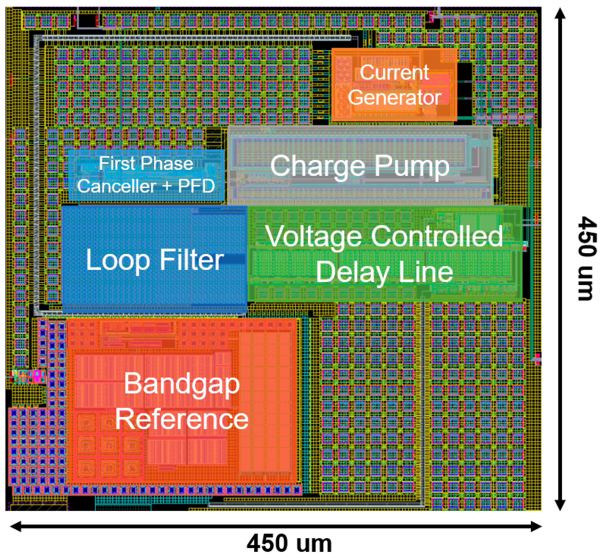
In Figure 12, the final simulation results show that the supply voltage of 1.2 V and the input reference clock used 30.72 MHz. Through the waveform of VCDL, which is the output of DLL, it was confirmed that the phase corresponding to 1/4 of the reference frequency was changed, and harmonic lock was prevented through the first phase canceller. After receiving the output of the VCDL, the edge combiner finally confirmed that it generated a frequency of 61.44 MHz through MUX and counter.
As suggested in this paper, the waveform was confirmed at 61.44 MHz through top corner simulation, Figure 13, and the same operation was verified without generating a harmonic lock during operation.
Table 1 represents the performance comparison of the proposed technique. It is designed to minimize power consumption, be sensitive to duty, and, as explained earlier, be highly sensitive to PVT (Process, Voltage, and Temperature) variations.

4. Layout

The total top layout size is 450 μm × 450 μm in Figure 14. If only the blocks involved in the operation of the clock doubler are included, the size excluding BGR and the current generator is 380 μm × 150 μm.

5. Conclusions

In this paper, we propose a multiplying delay-locked loop structure that is sensitive to PVT variation and generates a signal of double the reference frequency through the comparison of two input signals. Conventional circuits use the output of a delay circuit consisting of a reference frequency and the RC of a reference frequency as an input of an XOR gate. A delay-locked loop is used to implement a stable frequency multiplier because the delay circuit composed of passive devices and comparators used in the delay circuit is not sensitive to PVT. The final simulation results showed that the output frequency became 61.44 MHz, using a 1.2 V power supply and an input frequency of 30.72 MHz, and PVT operated normally. In this structure, by adjusting the delay cell inside the voltage-controlled delay line, it is possible to generate a frequency of a desired higher multiple other than double, and the input frequency can be set wider through the parallel capacitor. This process used the RF CMOS 55 nm process.

Author Contributions

Conceptualization, H.-W.K.; Writing—original draft, H.-W.K.; Writing—review & editing, H.-W.K. and S.K.; Supervision, K.-Y.L. All authors have read and agreed to the published version of the manuscript.

Funding

This research received no external funding.

Data Availability Statement

Not applicable.

Acknowledgments

This work was supported by Institute of Information & communications Technology Planning & Evaluation(IITP) grant funded by the Korea government(MSIT) (No.2019-0-00421, Artificial Intelligence Graduate School Program(Sungkyunkwan University)), and was supported by Korea Institute for Advancement of Technology(KIAT) grant funded by the Korea Government(MOTIE) (P0012451, The Competency Development Program for Industry Specialist).

Conflicts of Interest

The authors declare no conflict of interest.

References

  1. Reuben, J.; Anuroop, A.; Kittur, H.M. Clock frequency doubler circuit for multiple frequencies and its application in a CDN to reduce power. In Proceedings of the 2012 International Conference on Computing, Electronics and Electrical Technologies (ICCEET), Nagercoil, India, 21–22 March 2012; pp. 752–756. [Google Scholar]
  2. Hsueh, Y.-L. 28.2 A 0.29 mm2 frequency synthesizer in 40 nm CMOS with 0.19 psrms jitter and <−100 dBc reference spur for 802.11ac. In Proceedings of the 2014 IEEE International Solid-State Circuits Conference Digest of Technical Papers (ISSCC), San Francisco, CA, USA, 9–13 February 2014; pp. 472–473. [Google Scholar]
  3. Patel, K.I.; Gandhi, P.P.; Patel, N.D.; Prajapati, J. Voltage Controlled Delay Line with PFD for Delay Locked Loop in CMOS 90 nm Technology. IJRECT 2014, 1, 25–30. [Google Scholar]
  4. Raja, I.; Banerjee, G.; Zeidan, M.A.; Abraham, J.A. A 0.1–3.5-GHz Duty-Cycle Measurement and Correction Technique in 130-nm CMOS. IEEE Trans. Very Large Scale Integr. (VLSI) Syst. 2016, 24, 1975–1983. [Google Scholar] [CrossRef]
  5. Kang, K.T.; Kim, S.Y.; Kim, S.J.; Lee, D.; Yoo, S.S.; Lee, K.Y. A 0.33–1 GHz Open-Loop Duty Cycle Corrector with Digital Falling Edge Modulator. IEEE Trans. Circuits Syst. II Exp. Briefs 2018, 65, 1949–1953. [Google Scholar] [CrossRef]
  6. Megawer, K.M.; Elkholy, A.; Ahmed, M.G.; Elmallah, A.; Hanumolu, P.K. Design of Crystal-Oscillator Frequency Quadrupler for Low-Jitter Clock Multipliers. IEEE J. Solid-State Circuits 2019, 54, 65–74. [Google Scholar] [CrossRef]
Figure 1. The conventional clock doubler using XOR logic gate.
Electronics 12 02830 g001
Figure 2. DLL top block diagram.
Electronics 12 02830 g002
Figure 3. Top block diagram of MDLL.
Electronics 12 02830 g003
Figure 4. Schematic of voltage-controlled delay line.
Electronics 12 02830 g004
Figure 5. Normal operation of VCDL.
Electronics 12 02830 g005
Figure 6. (a) Schematic of first phase canceller and operation timing diagram. (b) Normal and abnormal operations according to the harmonic lock.
Electronics 12 02830 g006
Figure 7. Schematic of PFD.
Electronics 12 02830 g007
Figure 8. Schematic of CP.
Electronics 12 02830 g008
Figure 9. Edge combiner (a) block diagram (b) timing diagram.
Electronics 12 02830 g009
Figure 10. Simulation Result of MDLL without First Phase Canceller.
Electronics 12 02830 g010
Figure 11. Simulation of MDLL’s clock duty (a) 15% and (b) 75%.
Electronics 12 02830 g011aElectronics 12 02830 g011b
Figure 12. Simulation Result of MDLL.
Electronics 12 02830 g012
Figure 13. Top Corner Simulation Result of MDLL.
Electronics 12 02830 g013
Figure 14. Top Layout of Clock Doubler.
Electronics 12 02830 g014
Table 1. Performance Comparison with other related work.
Our Work[4][5][6]
Technology (nm)553505565
Clock Frequency(MHz)30.721~50333~100054
Duty Correction Extent (%)15~75-20~80-
Power Consumption (mW)0.4831.251.45
Chip Area (mm2)0.20250.00360.01860.07
Disclaimer/Publisher’s Note: The statements, opinions and data contained in all publications are solely those of the individual author(s) and contributor(s) and not of MDPI and/or the editor(s). MDPI and/or the editor(s) disclaim responsibility for any injury to people or property resulting from any ideas, methods, instructions or products referred to in the content.

