Review

Advances in Modeling and Suppression Methods of EMI in Power Electronic Converters of Third-Generation Semiconductor Devices

1
National Rail Transit Electrification and Automation Engineering Technique Research Center, Southwest Jiaotong University, Chengdu 611756, China
2
School of Electrical and Electronic Engineering, Harbin University of Science and Technology, Harbin 150080, China
3
Beijing Sinohytec Co., Ltd., Beijing 100084, China
4
State Key Laboratory of Automotive Safety and Energy, Tsinghua University, Beijing 100084, China
5
Department of Electrical Engineering Complexes, Novosibirsk State Technical University, Novosibirsk 630073, Russia
6
School of Mechanical Engineering, University of Science and Technology Beijing, Beijing 100083, China
7
Shunde Innovation School, University of Science and Technology Beijing, Foshan 528399, China
*
Authors to whom correspondence should be addressed.
Electronics 2023, 12(11), 2348; https://doi.org/10.3390/electronics12112348
Submission received: 25 March 2023 / Revised: 16 May 2023 / Accepted: 20 May 2023 / Published: 23 May 2023

Abstract

:
With the development of high-frequency, miniaturized, and lightweight power electronic devices, third-generation semiconductor devices are more and more used in the main circuits of power electronic converters. The electromagnetic interference (EMI) generated by their fast switching can affect the performance of power electronic converters. Therefore, it is necessary to investigate the modeling and suppression methods of conducted noise in power electronic converters of third-generation semiconductor devices. This paper describes the EMI sources and coupling paths of EMI in third-generation semiconductor devices used in power electronic converters. The modeling methods of EMI are summarized from the perspectives of power devices and coupling paths. The suppression methods of conducted noise are summarized by suppressing EMI sources and improving coupling path characteristics. This paper provides a reference for the electromagnetic compatibility design of power electronic converters for third-generation semiconductor devices.

1. Introduction

Traditional power electronic converters use semiconductor devices represented by silicon to realize energy conversion, but such devices have issues such as large loss, large volume, slow switching speed, and poor voltage and current resistance [1]. Therefore, power electronic devices composed of first-generation semiconductor devices have the issues of low conversion efficiency, large volume, and low operating frequency [2].
The third-generation semiconductor devices composed of silicon carbide (SiC) and gallium nitride (GaN) have higher blocking voltages, higher operating temperatures, and higher switching speeds than Si-based power electronic devices [3]. Taking a standard SiC device as an example, it is noteworthy that its blocking voltage is one order of magnitude higher than that of a Si device, its drift layer is thinner, its on-resistance is lower, there is no bipolar charge storage mechanism in it, and its switching dynamic behavior is greatly improved [4]. Compared with Si devices, SiC devices can reduce switching losses by 70% at the same switching voltage change rate. When third-generation semiconductor devices are used in new energy systems, their low loss characteristics can reduce the volume and weight of heat dissipation systems, and their high switching frequency characteristics can reduce the volumes and weights of passive devices. Therefore, third-generation semiconductor devices further promote the trend of high frequency usage and miniaturization in power electronics, and further improve the performance of power converters, which are considered to be the key driving forces for “carbon peak and carbon neutralization”.
The third generation of semiconductors can greatly improve operating frequency, reduce the volumes of devices and radiators, and increase power density in converters [5]. However, it must be noted that the high-frequency switching device is the main high-frequency noise source in a converter. The switching device generates electromagnetic interference (EMI) through the capacitive loop formed between the insulating sheet, the radiator, and the ground, bringing threats to the stable operation of the new energy system [6]. Therefore, the questions of how to improve the performance of third-generation semiconductor devices, reduce EMI caused by high switching frequency, and improve the electromagnetic compatibility of these systems have become the focuses of recent research.
This paper analyzes the EMI sources and coupling paths used in the third-generation semiconductor devices within power electronic devices. The EMI measurement and modeling methods used on third-generation semiconductor devices are reviewed. On this basis, the methods of suppressing EMI are summarized.
The structure of this paper is as follows. Section 2 analyzes the EMI mechanism and testing and analysis methods used on third-generation semiconductor devices in power electronic devices. Section 3 summarizes the methods of EMI modeling. Section 4 summarizes the EMI suppression methods. In Section 5, the electromagnetic compatibility research on power electronic devices is explored.

2. EMI Mechanism and Testing and Analysis Methods Used on Third-Generation Semiconductor Devices

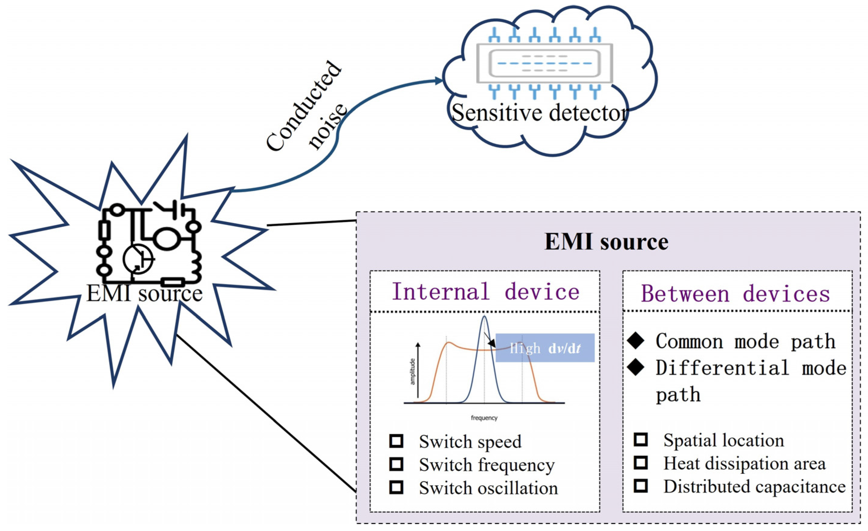
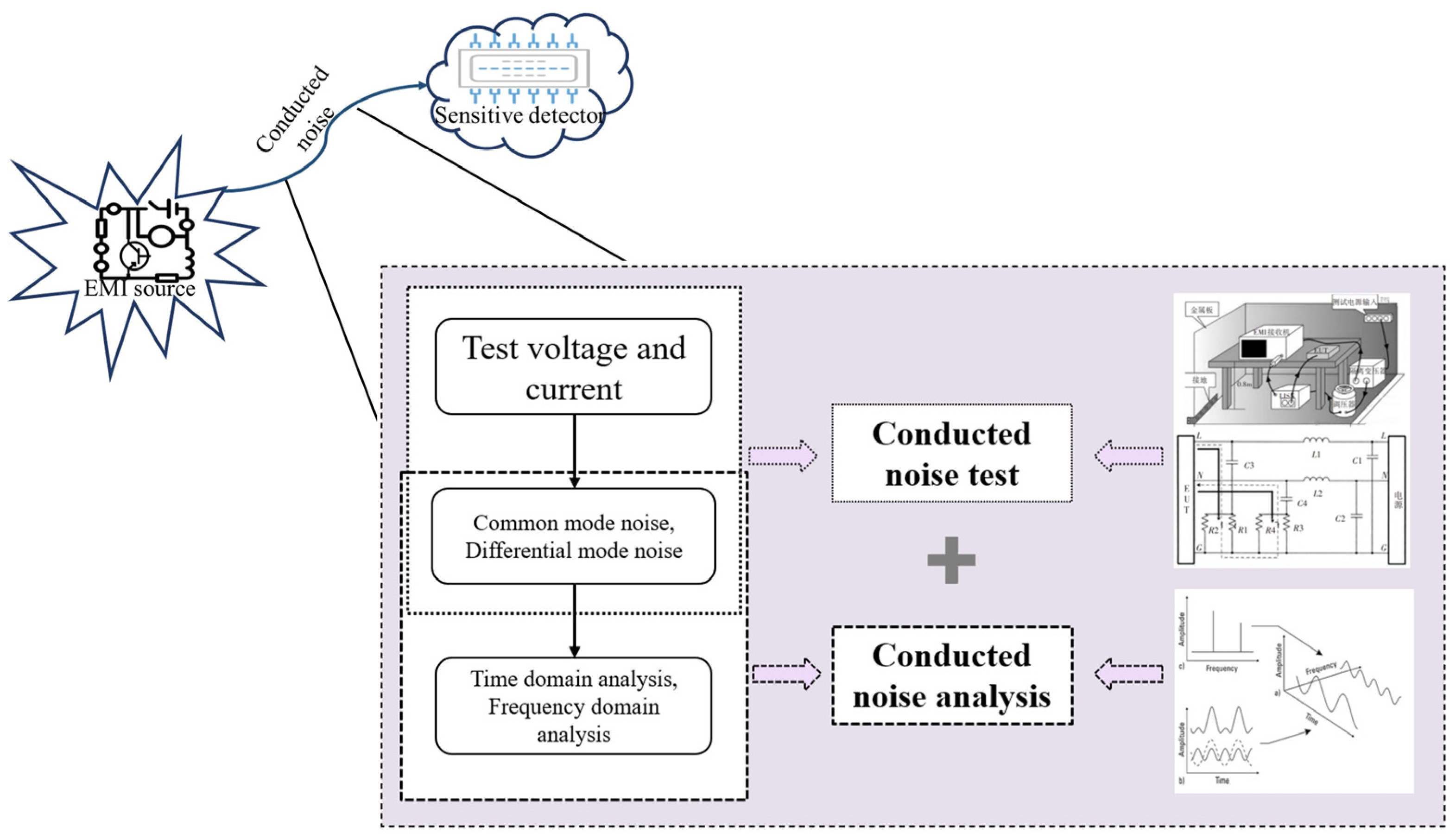
2.1. The Generation Mechanism and Coupling Path of EMI

The EMI caused by third-generation semiconductor devices is mainly concentrated in two aspects, noise sources and coupling paths, as shown in Figure 1.

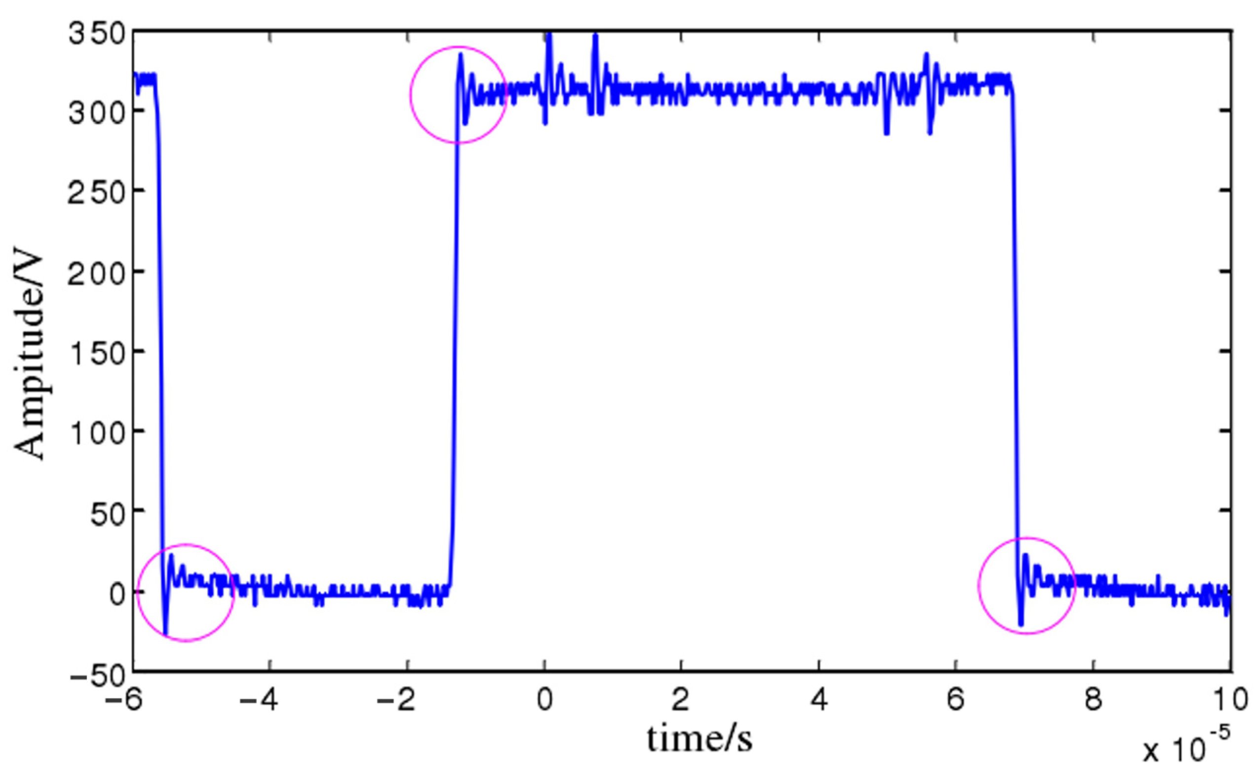
2.1.1. The Generation Mechanism of EMI Source

The high dv/dt caused by the high-frequency switching of a third-generation semiconductor device is the main source of EMI in a power electronic device. In addition, the parasitic capacitors between the ports and the loop stray inductors during the switching can cause the high-frequency oscillation of the gate source at high/low levels, as shown in Figure 2 [7].In these capacitors, the high-frequency oscillation accounts for a small proportion when the gate-source is at high or low level, and the dv/dt of the switching device is the main source of EMI.
In their study on EMI sources, Zhang et al. [8] pointed out that the fast-switching speed, high switching frequency, and ringing of SiC devices will increase the spectrum of EMI sources. Because SiC devices have a higher switching speed, higher switching frequency, and higher ringing than Si devices, the EMI noise generated by SiC devices will be higher than that generated by Si devices. Han et al. [9] analyzed the influence of third-generation semiconductor devices on the conducted noise characteristics of a system when applied in three-phase inverters. It was found that the high switching speed characteristic mainly affected the conducted noise in the high-frequency band of the system, and that the high switching frequency characteristic would improve the EMI in the whole conducted noise band. Wen and Dalal et al. [10,11] pointed out that the displacement current may be increased by several orders of magnitude due to the fast-switching transient and increased voltage amplitude of SiC MOSFET. When the displacement current is equivalent to the rated current of SiC MOSFET, the EMI and switching loss performance of the converter will be seriously deteriorated.

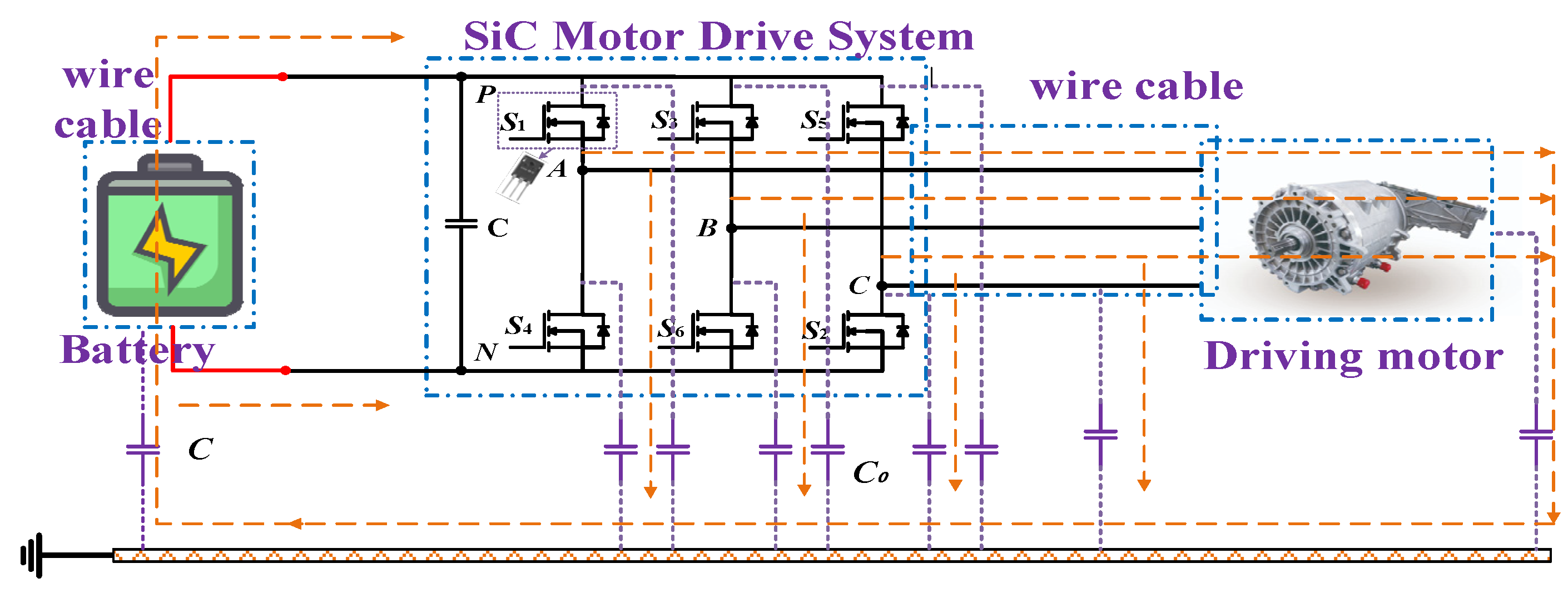
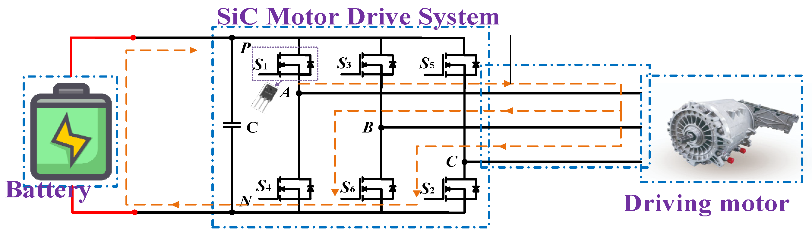
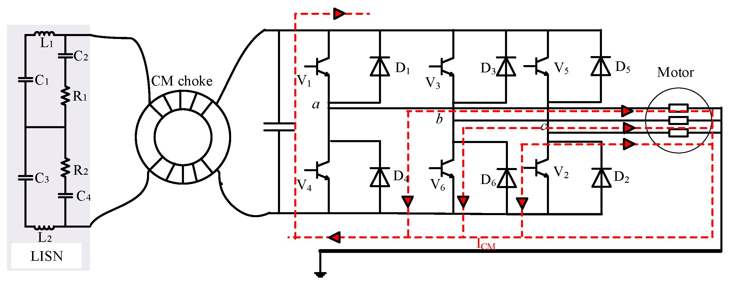
2.1.2. Propagation Characteristics and Coupling Path Analysis

The EMI of third-generation semiconductor devices is not only related to the switching behavior of power devices, but is also related to the parasitic coupling paths of power electronic devices. The peak of the EMI test spectrum usually comes from coupling path impedance resonance. The impedance characteristics of the coupling path are related to the circuit topology, grounding mode, and impedance characteristics of the system devices. Third-generation semiconductor devices do not change the EMI coupling path impedance characteristics of converter systems. Therefore, the analysis of the converter coupling path is still based on the analysis method used on first-generation semiconductors in power electronic devices. Based on the different EMI coupling channels, EMI is usually divided into common mode (CM) noise and differential mode (DM) noise, which correspond to the CM EMI coupling path and DM EMI coupling path, respectively.
CM noise is mainly formed by the interaction between the instantaneous dv/dt during the switching process and the parasitic capacitance inside a system. The parasitic capacitors in the system are mainly composed of the power source, the cable from the new energy system to the ground, and the radiator from the power electronic device to the ground. At the moment the switch turns on or turns off, dv/dt will act on the parasitic capacitors in the system to generate a large charge and discharge current, forming a CM current, and its flow path will flow through the ground and ground capacitors. A schematic diagram of this process is shown in Figure 3.
The DM noise of a power electronic device is formed by the interaction between the di/dt generated during the turn-on and turn-off processes and the stray inductors in the system. The stray inductors in the system mainly include the parasitic inductors of the pin, the inductors of the cable, etc. A diagram of the coupling path is shown in Figure 4.
As part of the research on coupling paths in power electronic devices that use third-generation semiconductors, Xie and Han [12,13] analyzed the coupling path impedance characteristics of SiC devices in Buck and Boost converters by using the transfer function method. The transfer function analysis method does not need to simplify a coupling path into CM and DM equivalent circuits. Instead, the node current equation and loop voltage equation are used on the equivalent circuit of the coupling path to analyze the impact of the transfer function characteristics of the EMI noise source of the converter system on CM and DM noise. Marlier et al. [14] used two equivalent models and a defined switching function to analyze the EMI coupling path in a system. The final results could be obtained by calculating the convolution of the switching function and the discrete results of each equivalent model. However, these studies were carried out at the system level, and the influence of the parasitic parameters of wide-bandgap devices on EMI cannot be analyzed from the perspective of packaging. Jia et al. [15] studied the influence of switching frequency, switching speed, and switching ringing on the conducted CM noise of a SiC electric vehicle powertrain. In the low-frequency band, the CM noise of the studied system increased significantly with an increase in the switching frequency. The switch ringing mainly affected the CM noise spectrum in the high-frequency band.

2.2. Analysis Method of Conducted Noise Characteristics of Third-Generation Semiconductor Devices

The noises of third-generation semiconductor devices mainly include conduction noise and radiation noise. This paper mainly discusses conduction noise. Conductive noise research focuses on two aspects of test methods and analysis, as shown in Figure 5.

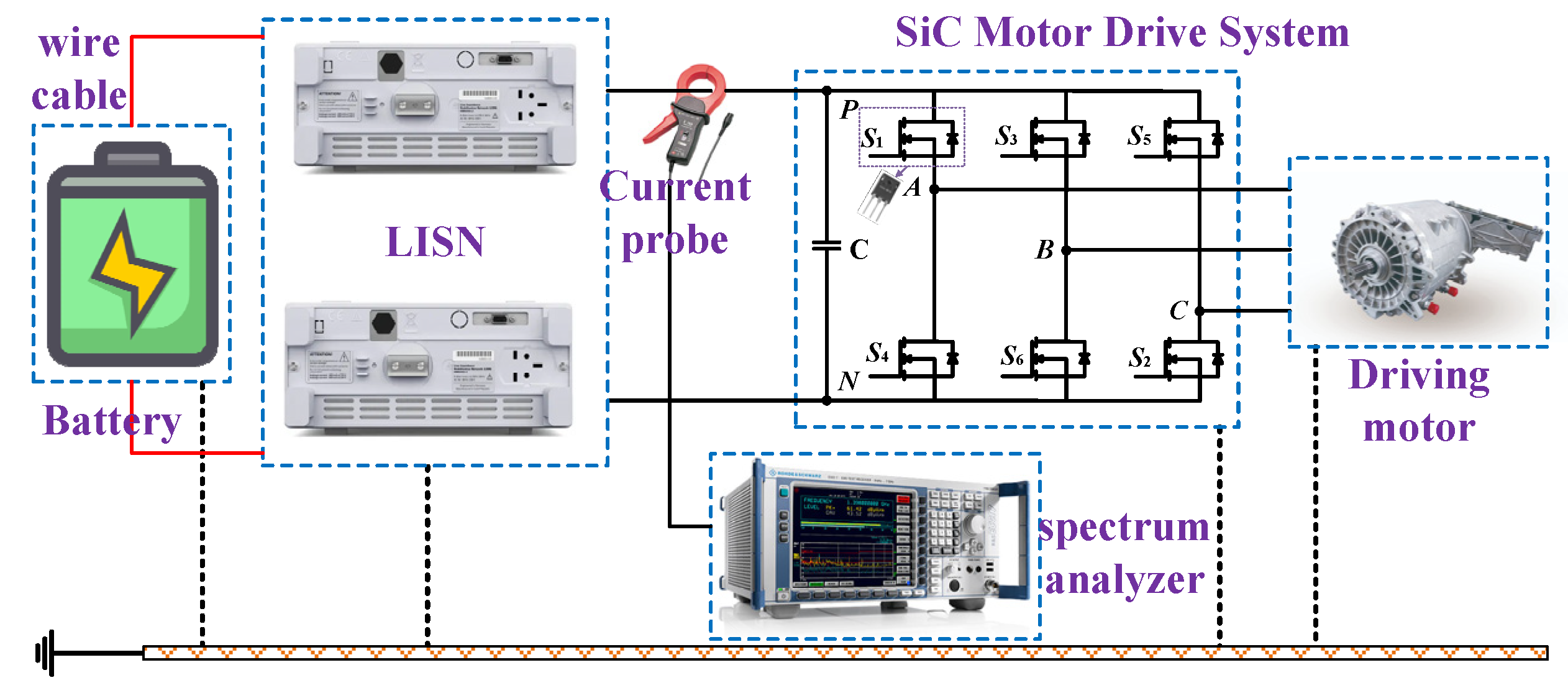
2.2.1. Conducted Noise Test Methods

A typical conduction test platform mainly includes the following: a Line Impedance Stabilization Network (Line Impedance Stabilization Network, LISN), spectrum analyzer, impedance analyzer, and EMI voltage/current probe. The test platform structure of a typical electric drive system is shown in Figure 6.
Within research on the EMI test platform and methods, Adamowicz et al. [16] proposed a test technology to characterize and extract parameters of ferrite EMI suppressors by using vector network analyzers and micro-strip test fixtures. The extracted EMI suppressor parameters in their study were compared with the data table values. Bandara et al. [17] investigated CM- and DM-conducted emissions without using a LISN. Using the switching power source as the device under test, the CM and DM impedances of the actual measurement device, with and without a LISN, were extracted; the study results better illustrated the influence of LISNs. Li. et al. [18] extracted the online impedance of an electrical system by treating their inductively coupled probe and the monitored electrical system as three cascaded two-port networks. Their method simplified the setting and calibration process, and could monitor the real-time impedance of the key electrical system in the study without interrupting the normal operation of the system, providing convenience for EMI research. Aiello et al. [19] studied the EMI sensitivity of a Hall effect current sensor, and compared the EMI stability of this non-contact device with that of the resistive current sensing method. The measurement results showed that the Hall effect current sensor was more affected by EMI than the resistive current sensing method. Lemmon et al. [20] created a specially designed hardware platform for evaluating the EMI behaviors of high-power systems based on third-generation semiconductor devices using custom metrics, providing a reference for the development of peripheral structures and the design of EMI mitigation components in future research.

2.2.2. Conducted Noise Analysis Methods

Conducted noise analysis methods for power electronic devices are mainly divided into two types: the time domain analysis method and the frequency domain analysis method. Conducted noise modeling can be done in PSpice and Saber. Both analysis methods require the modeling of EMI interference sources and EMI coupling paths, with the main difference between the two being in the modeling of EMI interference sources. The time domain analysis method focuses on using a detailed physical model and conducting the time domain waveform analysis of all devices [21]. Li et al. [22] compared the experimental results of time domain analysis and frequency domain analysis. The results showed that both methods were effective as long as the modeling was appropriate. However, with the increasing demand for computing resources and simulation time, the frequency domain analysis method is recommended as the preferred method for EMI analysis. The specific discussion of this topic is covered in Section 3.2.

2.3. The Effect of Temperature on EMI

Among wide-bandgap semiconductor materials, SiC has a much wider bandgap than Si and can handle higher voltages and faster switching speeds and show better efficiency [23]. On the other hand, GaN is particularly attractive for high-pressure, high-temperature, and high-pressure applications due to its higher electric field breakdown capability, good thermal conductivity, and high electron mobility [24]. The performances of wide-bandgap materials with Si are compared in Table 1 [25].
With the diversification of the working environment, researchers have been considering the influence of environmental factors on the circuit. The concept of electromagnetic robustness of chips was proposed by Ben in 2009 [26]. This researcher combined the problem of electromagnetic capacitance with the problem of semiconductor reliability. A microprocessor chip was subjected to experiments on high and low temperature aging and hot carrier injection. The relationships between negative bias, temperature instability, and hot carrier injection, caused by aging and the electromagnetic compatibility performance of the chip, were studied. Fernandez et al. [27] concluded that the electromagnetic sensitivity of CMOS was affected by negative-bias temperature instability. The mechanism by which electromagnetic interference and thermal stress affect semiconductor devices was explained in their paper. Dienot et al. [28] tested the PWM generation circuit and verified the effect of the combined stress of electromagnetism and heat on the function of the circuit. Wang et al. [29] proposed an efficient finite-difference time-domain (FDTD) algorithm for studying the frequency- and temperature-dependent characteristics of some graphene-based structures, with the auxiliary differential equation FDTD method and its conformal modification technique integrated together for handling atomically thin and electrically dispersive periodic geometries.

3. EMI Modeling Method

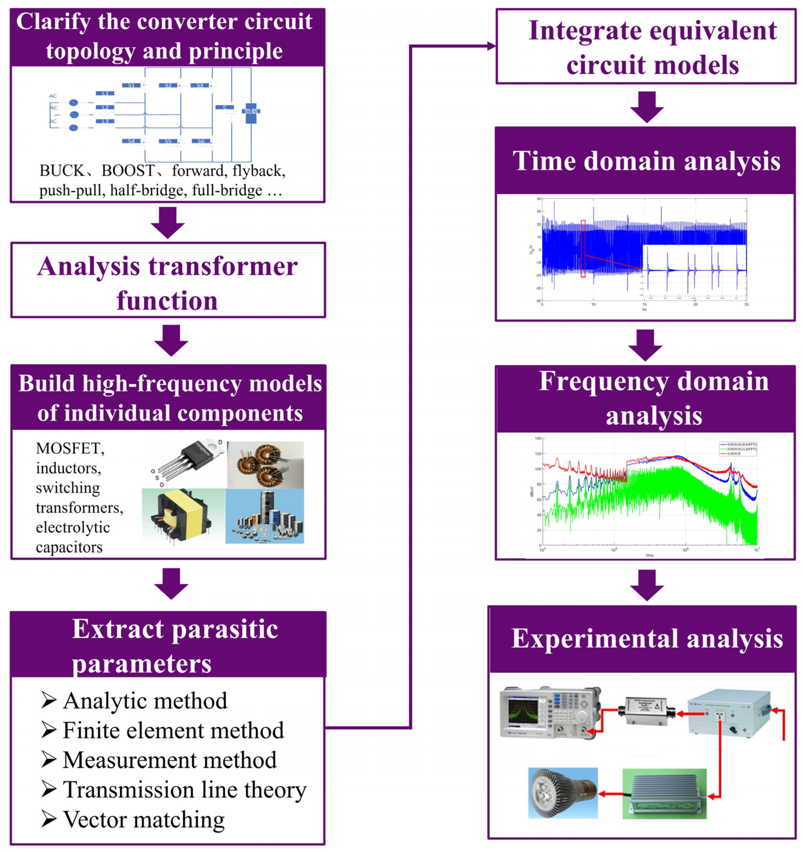
3.1. EMI Modeling Process

The basic process of conducting EMI modeling is as follows. (1) The circuit topology principle of the converter is clarified and the function of the converter is analyzed. (2) The high-frequency model of the component is established and the corresponding parameters are extracted. (3) The converter model is simulated in the simulation software. (4) The simulated EMI voltage and current spectrum are obtained via mathematical analysis. A flow chart of the modeling is shown in Figure 7. The flow chart mainly focuses on the modeling of the EMI source and the modeling of the coupling path of the parasitic parameter. On this basis, an equivalent circuit model is established. The technical difficulty of modeling lies in the extraction of the parameters of each component in the model.

3.2. Research Status of EMI Modeling

The high-frequency switching of third-generation semiconductor devices is the main factor required to generate switching EMI, and so the high-frequency modeling of the switching device must accurately simulate its transient characteristics [30]. The method used to model a switching device creates a circuit behavior model and a physical model. The physical model needs to partition the device according to the structure and function of the device. Depending on the carrier motion characteristics inside each sub-region, the device is described by physical equations. After that, under certain boundary conditions, the description equations are combined according to the current path to form a complete physical model of the device. An accurate physical model is helpful in order to describe the mechanism of the device [31,32]. The circuit model is modeled from the physical level of the device, and the parameters required for modeling here are mostly extracted via mathematical fitting. The relevant model parameters have no direct physical meanings. The circuit model can model a certain state of the device switching process, and can also model the whole device switching process. The circuit modeling method is relatively simple, and its modeling accuracy depends on the accuracy of parameter extraction. If the working conditions are inconsistent with the parameter-fitting conditions, the accuracy of the model will be significantly reduced. Willemen and Hsu [33,34] proposed an analytical model of MOSFET that used the parameters obtained from the device data tables and the parasitic parameters of the external circuit to simulate the high-frequency behavior of MOSFET. Y Yuan [35] proposed a MOSFET segmented behavior model that prioritizes runtime performance and convergence behavior, and is thus suitable for computer-based simulation analysis.

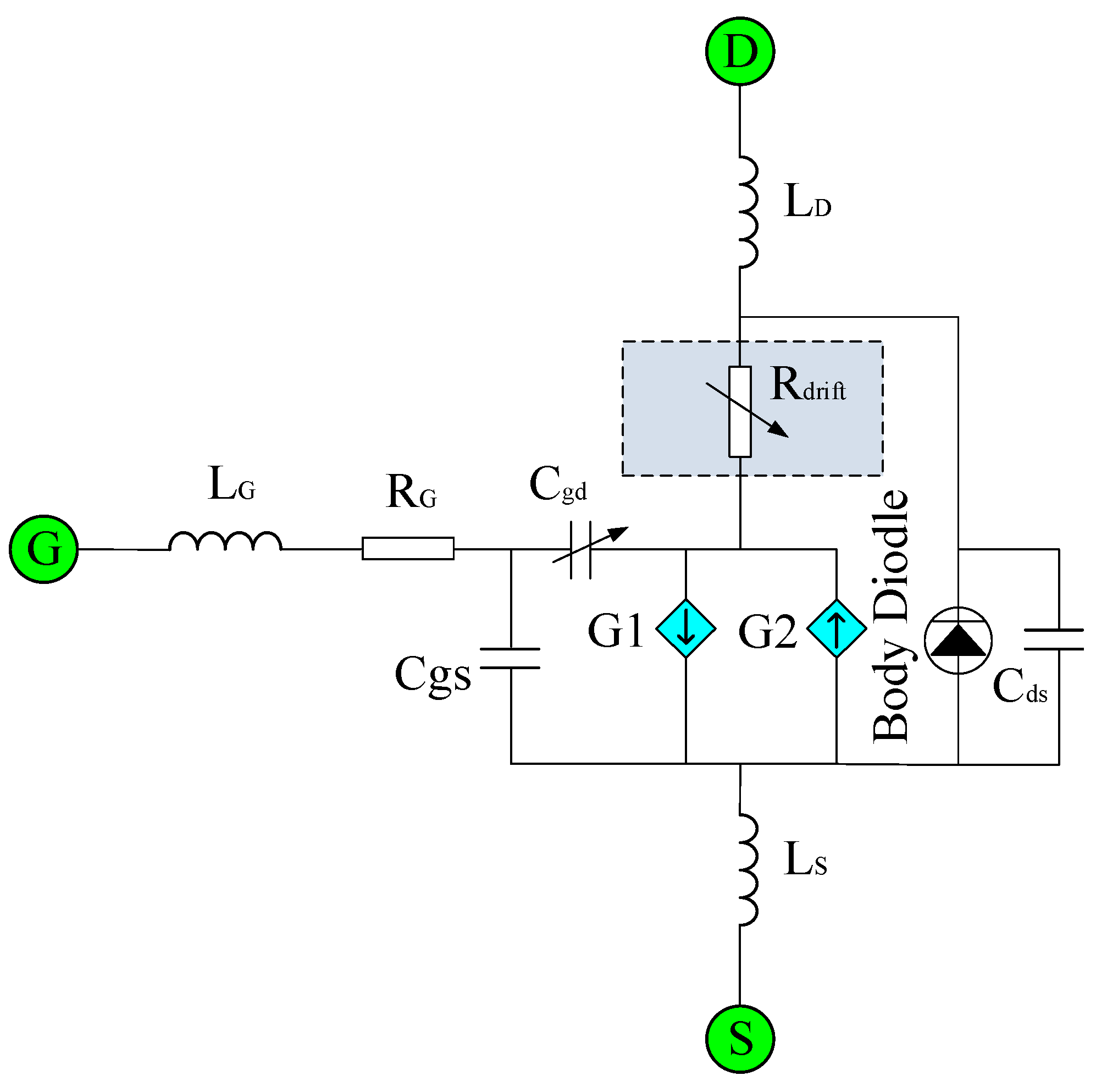
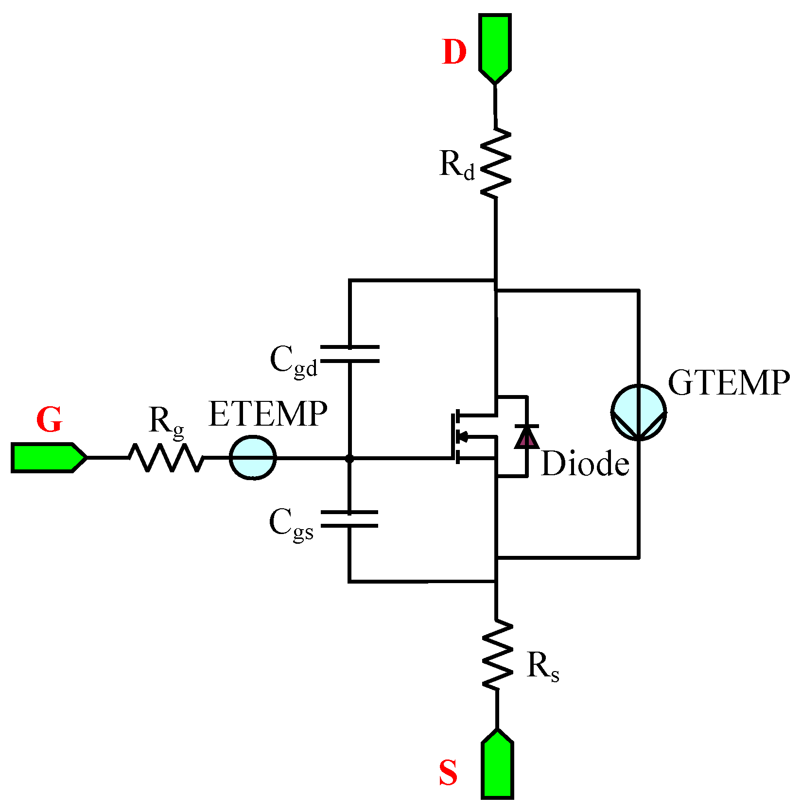
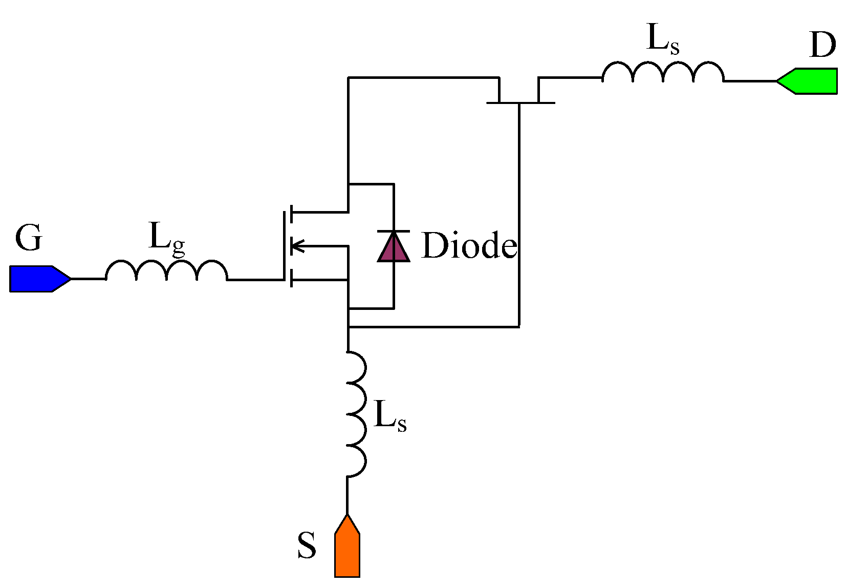
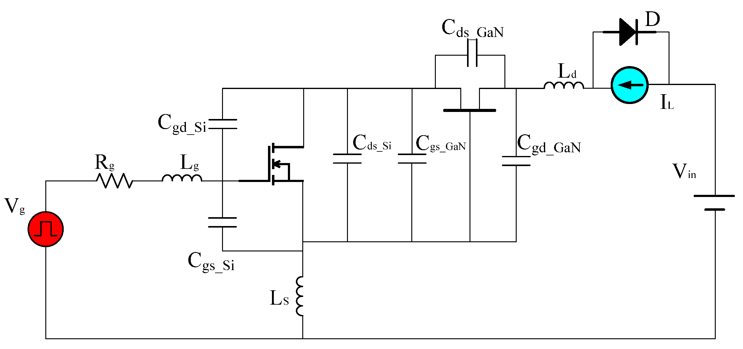
3.2.1. SiC Power Device Modeling

Device layer modeling is the basis of, and key to, SiC MOSFET research. Roccaforte and Smith [36,37] established the behavior model of SiC MOSFET, which is shown in Figure 8. The model consists of a drain-source resistance and three fixed parasitic inductors, and considers the influence of the parasitic inductors of the package on the model characteristics, but does not accurately simulate the SiC MOSFET switching process.
Merkert et al. [38] improved the behavior model of SiC devices by calculating the device loss, but their model did not consider the working mechanisms of the devices. Some scholars have tried to build a physical model of SiC MOSFET to clarify the working mechanism of these devices. The two described modeling methods are shown in Table 2.
Based on the theory of semiconductor physics, Wang et al. [40] used mathematical methods to express the internal mechanism of SiC MOSFET and constructed the device physical model. However, this model is complex, and its simulation takes a long time. Adamowicz and Johannesson [16,41] proposed a circuit-level model of SiC MOSFET based on the PSpice software by adjusting the parameters and modifying the model on the basis of the software’s own MOSFET core. The modeling focus changed from the internal mechanism of the device to the external characteristics of the device, but the model did not consider the influence of temperature and power loss. Xin et al. [42] proposed a variable-temperature SiC MOSFET model. The model uses a temperature-controlled voltage source and a current source to compensate the static characteristics of SiC MOSFET, and analyzes the operating characteristics of the device at different temperatures, but does not consider real-time power loss.
Wang et al. [43] proposed a behavior-level modeling method. Their model is shown in Figure 9, and the device behavior model was established by using temperature compensation fitting. In the cited paper, the Miller capacitor between the gate and drain, which was modeled by the complex Siemens model with parameter extraction, required a large number of parameters, bringing difficulties to modeling. Sun et al. [44] added a conduction model under gate negative pressure and negative temperature based on reference [43].

3.2.2. GaN Power Device Modeling

The device equivalent circuit, which uses GaN, is shown in Figure 10 [45]. As emerging devices, there have been relatively few studies on high-frequency models involving GaN power devices.
The high-frequency equivalent model that uses GaN is shown in Figure 11. Huang et al. [46] analyzed the steady-state parameters of the device in their study and compared them with Si MOSFETs at similar voltage and current levels. Pajnic et al. [47] analyzed the output characteristics of GaN devices. Their analysis results showed that GaN devices had the characteristics of high voltage, high switching frequency and low switching loss, and were thus suitable for high-voltage and high-current converters. Xie et al. [48,49] made a lot of simplifications in the switching process of the common gate-source structure device, and believed that the parasitic inductors between the low-voltage Si MOSFET and the high-voltage GaN HEMT were key to affect the switching characteristics of the device. Carrasco et al. [50] applied GaN HEMT to single-phase inverters. The switching process of the device in application was analyzed in their paper, but the expression of voltage/current and switching loss were not further analyzed. Garsed et al. [51] proposed a simplified analytical model of the switching process in GaN devices. However, the influence of stray parameters and reverse recovery—which are quite different from the actual current and voltage stress and switching loss— on the switching process were not considered.
Liu et al. [52] established a loss analysis model for high-voltage GaN devices. Their model can accurately describe the switching process of a GaN device and can accurately analyze its output characteristics, transfer characteristics, and driving characteristics. The simulation and experiment in the paper were in good agreement. Huang et al. [53,54] analyzed the parasitic parameters inside the cascaded high-voltage GaN device in detail. By changing the installation position of the internal low-voltage Si MOSFET and the high-voltage depletion GaN device, the parasitic parameters inside the device were effectively reduced and the reliability of the device was improved in this study. Parikh and Chen [55,56] applied high-voltage GaN devices to Buck and LLC converters to evaluate their performance advantages. However, the influence of the differential packaging of GaN devices on the driving circuit was not analyzed in the paper, and the advantages of high voltage GaN devices and Si MOSFET in LLC resonant converters were not explained.

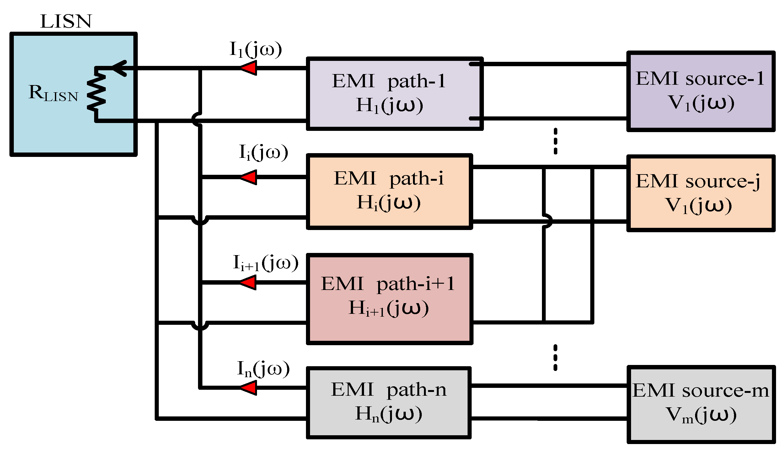
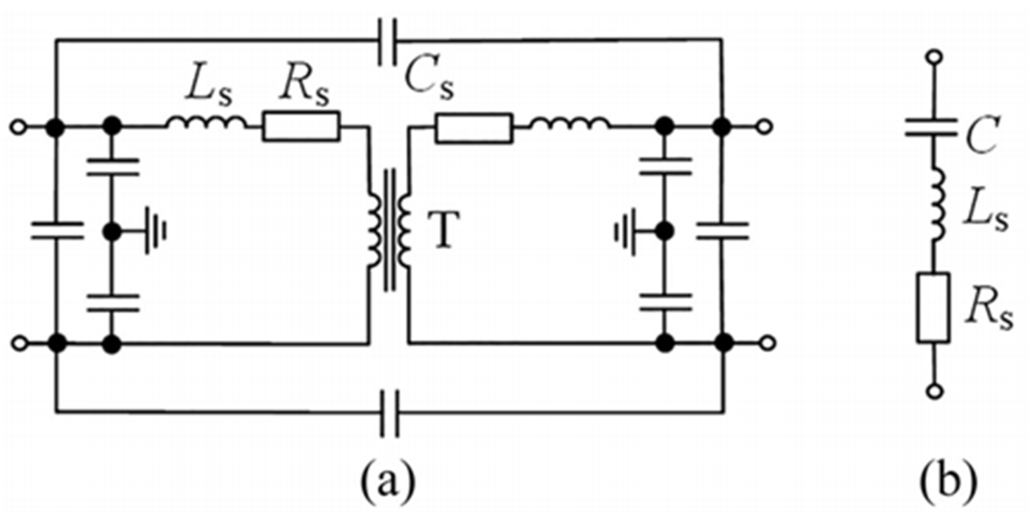
3.3. Conducted Noise Coupling Path Model

Conducted EMI propagates in the circuit in two modes: DM and CM. The coupling path includes not only the circuit composed of power devices, but also the circuit composed of parasitic elements and distributed elements [57].
The experimental results of a conducted EMI test are the sum of DM noise and CM noise. Due to the fact that EMI sources and coupling paths are different in DM noise and CM noise, it is necessary to analyze these two kinds of noise separately, and establish the DM and CM noise models of power converters. Since the modeling of the coupling path needs to be analyzed according to different circuit topologies, only the general modeling method is described here.
When modeling the conductive electromagnetic coupling loop, it is required to accurately find out the CM and DM noise coupling paths in the topology. When the converter contains multiple EMI sources and coupling paths, a multi-channel parallel analysis method should be adopted, as shown in Figure 12. Then, the circuit simulation software will be used to simulate the time domain, the time domain waveform of the noise voltage will be decomposed by Fourier, and finally, the spectrum of the conducted EMI will be obtained [58].
The main models created via conduction coupling path modeling include the time domain model and frequency domain model. The aim of the time domain model is to put a high-frequency model of all devices into the circuit in order to simulate the transient waveform, and the obtained model is relatively complex. Since the time domain model does not deeply analyze the mechanism underlying the generation and propagation of conducted EMI, it is impossible to judge which parasitic devices are the main ones, and instead, the parasitic parameters of all devices are blindly extracted [59]. Therefore, the model accuracy of the time domain model is poor. Frequency domain modeling is a modeling method used to obtain the EMI spectrum via frequency domain calculation involving the EMI source. When the frequency domain model is simulated, the high-frequency model of the EMI source should be established, and then the coupling path of the EMI should be analyzed [47]. Considering that the parasitic parameters of passive devices have a great influence on the results of frequency domain prediction, the coupling path model [60] should be established based on the high-frequency model of passive devices. Then, according to the EMI source model and the coupling path model, the EMI value of the whole loop will be obtained. Finally, the obtained DM EMI and CM noise will be superimposed, yielding the EMI spectrum of the system.

3.3.1. Time Domain Model

The time domain analysis method is based on using the physical structure or behavior model of third-generation semiconductor devices to characterize EMI sources. In this method, circuit simulation software is used to simulate a whole converter system, and the EMI spectrum distribution of the system is obtained by using discrete Fourier transform. The accuracy of the time-domain simulation model mainly depends on the accuracy of the power device model. At present, a lot of research has been carried out on the simulation model of third-generation semiconductor devices. The mainstream method involves obtaining the behavioral-level circuit simulation model by fitting a manual chart of the device data or experimentally measured parameters by using software tools. However, circuit design engineers may not be able to obtain all the experimental test parameters required to establish this model for third-generation semiconductor devices, and the stability and convergence of the current device simulation model still need to be verified when the model is applied to the simulation of EMI in power electronic devices. Due to the fast-switching speeds of third-generation semiconductor devices, the time-domain-simulation step is usually set in a few nanoseconds to simulate the transient process of switching, and so, the time-domain simulation method still has the problem of long simulation time. In summary, the time-domain simulation analysis method has the disadvantages of non-convergence and long simulation time, and so it is difficult to use it for the parametric analysis of EMI characteristics and suppression measures in power electronic devices. Within research on the time domain analysis of power electronic devices, Duan and Dillan [61,62] proposed a simple modified SiC MOSFET behavior model using the SPICE language. In their paper, the key parameters of the model were analyzed and determined in detail, and the main parameters of the switch dynamic characteristic in the model were compared with the measured results. The results showed that the modified model had higher accuracy than the actual measurement results. Duan et al. [63] modeled the EMI source and coupling path of the conducted noise of a full SiC three-phase inverter, and predicted the conducted noise at the power port by using time-domain simulation and fast Fourier transform. In the frequency range of 10 kHz–30 MHz, the simulation results were basically consistent with the measured results. On the basis of establishing a system-level conducted electromagnetic interference model for an entire SiC-based electric vehicle powertrain, Jia et al. [64]. analyzed the influence of AC cable length, AC cable type, DC cable type, and other system layout characteristics on common-mode electromagnetic interference noise through the time-domain simulation of the system-level conducted electromagnetic interference model. Zhang et al. [65]. established a conducted noise model using the measured output voltage and the model of passive devices. This model used a time-domain approach. The measured output voltage of one of the Zhangbei projects was used as the excitation source for the simulation. The model of the inductor and transformer is depicted in Figure 13, where the conducted noise amplitude on the AC side is seen to be reduced by approximately 44 dBμV/Hz.

3.3.2. Frequency Domain Analysis

The frequency domain analysis method applies the superposition principle to linearize the nonlinear power electronic circuit. The time-domain switching waveforms of the power device are obtained by conducting simple experimental tests, and the spectrum description of the EMI source is obtained via discrete Fourier transform. The frequency domain modeling method, which has the advantage of fast simulation speed, can be used to analyze the EMI characteristics of a system and optimize the design of its EMI filter. The disadvantage of this modeling method is that it allows only one EMI source to be analyzed at a time.
As part of the research on the frequency domain analysis of power electronic devices, Revol et al. [66] replaced the switches of an inverter with current or voltage sources defined in the frequency domain. Their method considered all passive devices and achieved fast and stable simulation. Their experimental results showed that the calculation results of the model were in good agreement with the experimental results in the bandwidth range of 150 kHz–30 MHz, and that the frequency domain analysis method significantly shortened the simulation time. Li et al. [67] proposed a hybrid packaging structure SiC half-bridge power module with ultra-low parasitic inductors and low parasitic capacitors to ground. The low parasitic inductors could improve the switching speed, and the low parasitic capacitors could suppress the grounding current. Liu et al. [68] proposed a new frequency-domain method to predict conducted EMI in DC-AC converters with varying switching conditions during operation. Their method was based on the equivalent module terminal behavior frequency domain EMI source model of a switching cycle at a given operating point, and the module terminal behavior models of different operating regions were superimposed in the frequency domain to predict the conducted EMI of the entire operating cycle. Duan et al. [69] proposed a frequency-domain method for predicting the DM EMI of three-phase SiC inverters. Their calculation and experimental results showed that the proposed frequency domain calculation results were in good agreement with the experimental results in the switching frequency range and the resonant frequency range. Zhou et al. [70] proposed a new frequency-domain EMI modeling technique. In their paper, based on the frequency domain model, a three-terminal behavior model for analyzing mixed model EMI was derived. Differing from the traditional behavior model, the DM and CM EMI sources were independent of each other, and this helped readers to intuitively understand the mixed model phenomenon.

3.4. Comparison of Time-Domain and Frequency-Domain Modeling Methods

The two modeling methods are shown in Table 3.
Elrayyah et al. [73] studied the EMI paths of conducted EMI in DC/AC inverters, using fast Fourier transform (FFT) to simulate the EMI spectra. However, when analyzing CM noise, the error between the high-frequency band and measurement result was large, and there was a convergence problem. Hedayati et al. [74] directly used the frequency domain analytical method to establish a prediction model: that is, the circuit equation of the EMI source and the coupling path was obtained in the paper, and this equation was converted into a transfer function by using the mathematical method. However, for more complex circuit topologies, it would be difficult to directly obtain the transfer function of EMI, and so this method is only suitable for simple topology. Tang et al. [75] proposed a prediction model of conducted EMI based on Thevenin’s theorem for a three-phase motor drive circuit and constructed the equivalent circuit of the CM conduction path and DM conduction path. The frequency domain analysis results from their study show that their method had high accuracy in predicting conducted EMI. Han et al. [9] used the spectral analysis method to analyze the CM noise of a motor drive system. A frequency domain prediction model in the range of 10 KHz–30 MHz was established. It simultaneously solved the convergence problem in the time-domain simulation and shortened the simulation time.

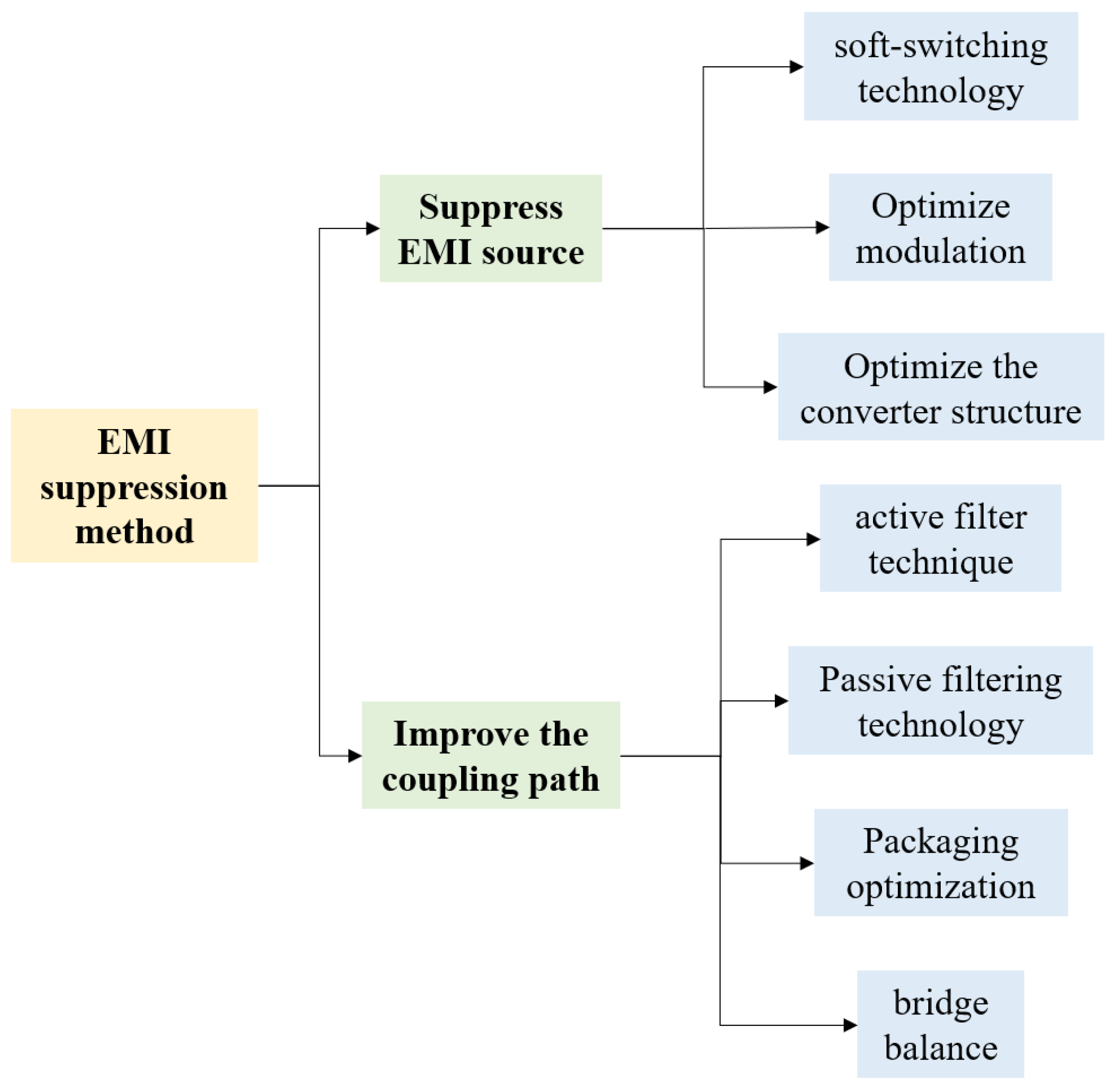
4. Study on EMI Suppression Methods for Power Electronic Devices

The existence of high dv/dt EMI sources and couplings in the conduction paths are the root causes of EMI in power electronic devices [76]. Therefore, the research on EMI suppression methods is mainly divided into two categories: one aims to suppress EMI sources, and the other aims to improve coupling path characteristics. The main measures to suppress an EMI source are the use of soft-switching technology, the optimization of the modulation mode, and the optimization of converter topology. The main measures to improve a coupling path involve active filtering technology, passive filtering technology, packaging optimization layout, and bridge balancing technology. These EMI suppression methods are classified as shown in Figure 14 [77].

4.1. EMI Suppression Strategy for Suppressing EMI Sources

4.1.1. Soft-Switching Technology

Soft switching improves EMI noise by reducing the dv/dt and di/dt generated by system power devices. Soft-switching technology requires a corresponding soft-switching scheme according to the circuit topology of the application. Some soft-switching characteristics in power conversion systems are susceptible to perturbations by system parameters, which can affect EMI suppression [78] Third-generation semiconductor devices work at high frequencies. Their turn-on will have higher voltage and current overshoot and oscillation than Si-based semiconductor devices. Soft-switching technology can suppress the amplitude of voltage and current overshoot and oscillation, and effectively reduce the DM noise in the high-frequency bands of power electronic devices, but it has no obvious effect on the DM noise in low-frequency bands. Kim et al. [79] proposed a closed-loop gate driver to control di/dt and dv/dt that reduces the amplitude of high-frequency conducted EMI. Xie et al. [12] proposed a soft-switching circuit to suppress conducted EMI: that is, parallel RLC circuits were added at both ends of switches to reduce the switching loss in order to achieve the purpose of suppressing EMI. It was concluded that the amplitude of low-frequency current noise under CCM was small, but the amplitude of high-frequency current noise was higher than that under DCM.

4.1.2. Optimization of Modulation

Pulse width modulation is the main factor that determines power electronic noise. Modulation technology can improve the output voltage waveform quality of the inverter and suppress the conduction noise in a system. The optimization of the modulation method aims to directly adjust the generation process of the EMI source and thereby reduce the noise in the low-frequency band. Xiang et al. [80] proposed that EMI current can be suppressed by using CCM and TCM. By comparing the influences of the two methods on EMI, it was concluded that the current noise amplitude of CCM was smaller in the low-frequency range, but the current amplitude was higher than that of TCM in the high-frequency range. Xie et al. [81] used the RPWM strategy instead of the traditional SVPWM strategy. In their study, the volume of the filter inductor was effectively reduced by combining the passive filter. Therefore, the EMI current of the whole frequency band of the controller met the requirements. Omar et al. [82] proposed the use of different pulse random modulation techniques to increase the power spectral density in order to suppress conducted EMI. Natarajan et al. [83] derived a formula for calculating the power spectral density to predict EMI. Mihalic et al. [84] compared the effects of four methods—random pulse position modulation, random pulse width modulation, fixed duty cycle random carrier frequency modulation, and variable duty cycle random carrier frequency modulation—on the power spectral density and EMI of a DC-DC synchronous rectifier. It was concluded that random pulse width modulation and fixed duty cycle random carrier frequency modulation had the best effects in terms of suppressing the DC-DC converter. Dove et al. [85] transferred harmonic power with high amplitude to other frequencies by utilizing random pulse width modulation technology, and reduced the power of the previous harmonics. According to the probability distribution function, the switching behavior of the DC-DC converter was designed to eliminate EMI optimally. Hasan et al. [86] proposed a hybrid pulse modulation technique that modulated pulse width and pulse position in each pulse modulation period. EMI was effectively suppressed in a quasi-Z source converter composed of an impedance source network and a GaN device. Vedet et al. [87] proposed a pulse width modulation strategy to eliminate the CM voltage of the three-phase AC-DC-AC converter. In this strategy, the inverter and the rectifier worked at the same switching frequency, and the inverter and the rectifier switched synchronously to offset the CM voltages of the two converters.
Compared with the filter method, the pulse width modulation method has the advantages of not increasing system cost and design difficulty, and has high versatility for systems with different power levels. Due to the change in control mode that it incorporates, this method will adversely affect inverter output voltage.

4.1.3. Converter Structure Optimization

In a converter, the PCB layout, and device structure optimization, suppress EMI by varying the noise transmission path and system impedance, respectively. By optimizing the main circuit topology of the power electronic converter, the CM EMI source of dv/dt can be offset, thereby reducing the conduction EMI. The method of counteracting the EMI source fundamentally suppresses EMI, and its EMI suppression effect is more significant than those of other methods. Based on the existing research on DAB converters, a parallel dual DAB structure based on active neutral point clamping was proposed by Xie et al. [84]. The dv/dt in their paper was offset by controlling the on-off setting of the switch to reduce the EMI caused by the CM current. However, this increased the cost and reduced the power density of the system. Kumar et al. [88] adopted a split-winding structure. The inductance windings were redistributed at the input and output terminals to optimize the potential of the nodes in the circuit. The inverse dv/dt node was established to eliminate CM noise. Xie et al. [89] proposed a CM voltage offset method that eliminated the CM voltage of the converter by inserting a compensation voltage source into the input power cable of the converter. Li et al. [90] analyzed and determined that the parasitic capacitance of power devices to the ground was the main factor affecting common-mode interference. They increased the thickness of the thermal grease between the thermal conductive sheet of the power device and the heat sink, thereby increasing the parasitic impedance of the switching device to the ground and effectively reducing the low-frequency conduction noise of the converter system. Their method can reduce the volume of the converter, and its implementation cost is low; thus, it has engineering application value.

4.2. EMI Suppression Strategy to Improve Coupling Path Characteristics

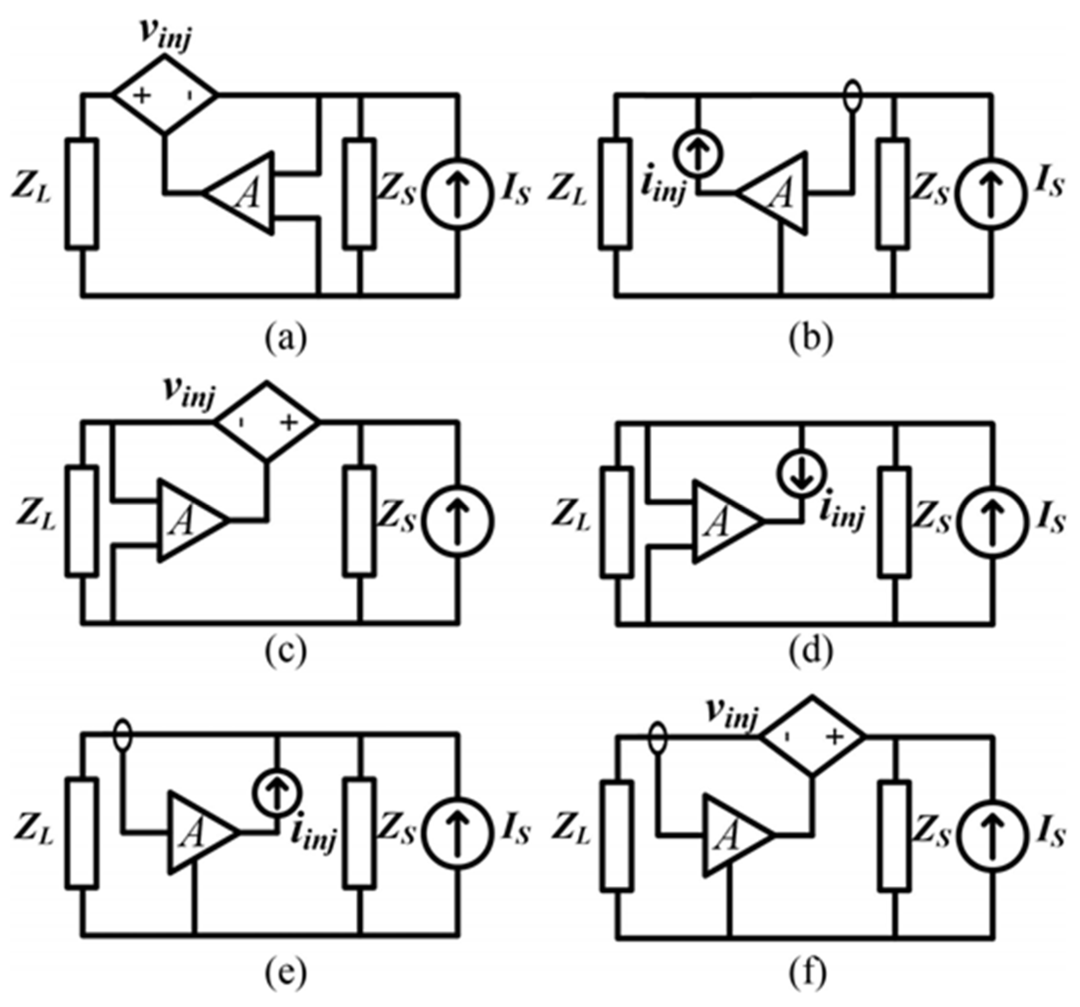
4.2.1. Active Filtering Technology

Active filtering technology detects CM current in real time. The emitter follower is used to generate reverse CM voltage or CM current. The reverse CM current is injected into the converter to suppress the conducted EMI. There are three main parts of an AEF circuit. These are the noise-sensing circuit, noise-processing active circuit, and noise-injection circuit. Conventionally, the noise-processing active circuit involves an amplifier stage that is capable of driving the injection stage. Zhang et al. [91] proposed an active common noise canceller. Their method first detected the CM voltage or current from the coupling path, then used the amplifier circuit to generate reverse voltage or current. Finally, the reverse signal was injected into the circuit. The suppression of CM noise was realized. Fan and Bendicks [92,93] solved the problem of signal path delay in an active filter system by using a synthetic cancellation signal. Their experimental results showed that the synthetic cancellation signal had an obvious suppression effect on EMI in a specific frequency range. Adapa and Mueller [94,95] proposed an active filter technology, based on the generalized predictive pulse compensation method, wherein the EMI generated by a DC-DC converter was suppressed by the half-bridge gate drive circuit. The effectiveness of the method was verified on a Buck converter with a simulated output controller.
A combination of different noise-sensing and noise-cancellation methodologies yields the conventional AEF as shown in Figure 15 [76]. In addition, according to whether noise detection is completed on the source side or on the load side, the control scheme can use feedforward or feedback. AEF itself is a single-order filter. Due to the bandwidth limitations of the Detection, Processing, and Elimination stages, AEF is designed to provide noise attenuation from the EMI frequency range (150 kHz, according to the International Radio Interference Standards Special Committee) to several MHz. In order to provide noise attenuation in a higher frequency range, another passive component must be used. This passive element is combined with AEF to form HEF. The higher the attenuation and bandwidth provided by AEF are, the smaller the additional passive components required to form HEF become. The choice of specific AEF topology depends on the source impedance and load impedance [96].

4.2.2. Passive Filtering Technology

Passive filtering technology is the most widely used EMI suppression technology in existing power electronic devices. It eliminates the resonance point of a converter by changing the impedance characteristics of the coupling path to suppress EMI conduction noise. The research on passive filters mainly focuses on three aspects: reducing filter sizes, increasing the number of DM inductors, and reducing the external leakage flux of the filters.
Fan et al. [92] proposed a method of adding a passive device absorption circuit. This method used ferrite magnetic beads and an improved gate driver to minimize EMI sources. Zhang et al. [4] proposed that the parasitic parameters of EMI filters seriously deteriorated the high-frequency performance of the filters. A method of introducing resistors into the CM coupling path to improve filter performance and reduce EMI was proposed. A conducted CM EMI suppression method based on an independent floating radiator was proposed. It suppressed high-frequency CM EMI by improving the electromagnetic source and coupling path in the central mode. Chu et al. [97] compared the EMI spectrum before and after adding the CM inductor. It is proposed here that adding CM inductance between LISN and the converter can effectively suppress the CM current. The implementation plan is shown in Figure 16. Dai et al. [98] proposed a new integrated multi-function CM choke based on an EMI filter. It combined a current transformer and a common choke into one element. This versatile CM choke eliminated the need for current transformers to optimize the topologies of hybrid EMI filters. Han et al. [9] paralleled the X-type capacitor on the input DC filter capacitor and added a pair of Y-type capacitors between the high-voltage positive and negative buses on the PCB board and the ground to suppress EMI. Their results showed that this method could effectively suppress the conducted EMI in the range of 150 kHz–108 MHz. Tanim et al. [99] suppressed CM EMI by adding a CM choke to the Wheatstone bridge. Their experimental results showed that this method had the characteristics of reducing EMI noise and having easy-to-realize soft switching. Dai et al. [100] proposed two methods to suppress CM EMI in AC-DC-AC converters. In the first, a CM choke was added. A three-phase CM choke could be installed on the grid side or on the load side, and a two-phase CM choke could be installed on the DC side. In the second method, the Y-type filter capacitor was added, and the filter capacitor CapN connected the neutral points of the filter capacitor on the rectifier side and the inverter side. The Y-type filter capacitor was connected in series with the line-equivalent inductance to form a path to reduce the CM current and suppress EMI. Hedayati et al. [101] designed CM filters based on LCL filters. Filter inductors and filter capacitors were inserted at the AC three-phase input in the study. At the same time, capacitors Cy1 and Cy2 were inserted at the middle bus of the rectifier and the inverter of the AC-DC-AC converter for filtering. In addition, the connection point of the two capacitors in the CM filter was connected with the three-phase filter capacitor of the LCL filter. The capacitor CMg was introduced between the connection point and the ground to make it as close as possible to the ground potential, thereby improving the filtering efficiency.

4.2.3. Optimization of Package Layout

The package parasitic inductors have a great influence on the EMI sources in converters. Reducing the package parasitic inductors can not only suppress the switching voltage ringing, but also improve the switching speed of power electronic devices [102]. In addition, the parasitic CM capacitors of the package determine the impedance characteristics of the CM EMI coupling path. Reducing the parasitic CM capacitance of the package is an effective means by which to reduce system EMI. Through improved thermal management and packaging material processes, higher power densities and wider temperature ranges (i.e., operating temperatures above 200 °C) can be supported. Ultra-low inductance packaging can protect components from voltage transients and suppress EMI.
Bendicks et al. [103] proposed a hybrid half-bridge SiC power module and a hybrid half-bridge for TO-247 packaged SiC devices. Their proposal effectively reduced the total number of parasitic inductors and achieved the purpose of reducing EMI. Pahlevaninezhad et al. [93] proposed a high-frequency planar transformer for DAB converters. Its embedded EMI filter could effectively eliminate CM EMI in a DAB converter. Kumar et al. [104] proposed a low-inductance bus design method for discrete devices. This method could effectively reduce the coupling inductance in the loop, and in turn, high-frequency EMI could be better suppressed.

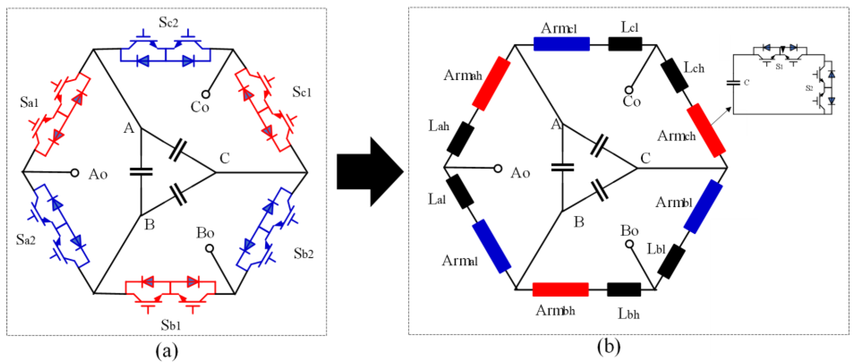
4.2.4. Bridge Balancing Technology

Bridge balancing technology uses the Wheatstone bridge balancing principle to construct the converter as a Wheatstone bridge. The impedance of the converter is matched to meet the bridge balance conditions, thereby eliminating the CM current of the converter and suppressing conducted EMI. Bridge balancing techniques require the adjusting of impedance parameters multiple times in order to achieve bridge balancing. In addition, for occasions in which a converter is required to be common ground, bridge balancing technology will destroy the common-ground characteristics of the converter. Additionally, its actual suppression effect is debatable.
Narayanasamy et al. [105] derived two CM noise sources and their characteristics and proposed a CM noise reduction technology with a large impedance ratio balanced bridge to achieve EMI suppression. Chen et al. [106] proposed a neutral-point clamp topology with bridge balancing technology that could achieve large EMI attenuation and reduce filter parameters to reduce size and weight. Yang et al. [107] proposed a CM equivalent circuit model of a multi-unit AC/DC traction system in which two series balanced capacitors CB were incorporated at the input end, and the midpoint of the balanced capacitor was connected to the midpoint of the two DC buses to suppress EMI. Yang et al. [108] grounded the inverter casing with the inverter and the motor at the same time, and decoupled the inductor LG in series to reduce the influence of the inverter on the CM noise of the rectifier, so as to reduce the CM noise of the system. Li et al. [109] changed the traditional three-phase hexagonal AC chopper bridge arm to multiple chopper AC voltage regulation circuits and inductors in series, as shown in Figure 17. A multistage AC hexagonal chopper, which reduced the dv/dt generated by the switching device, was formed so as to effectively reduce EMI.
Table 4 summarizes the advantages, disadvantages, and use cases of several EMI suppression methods.

5. Future Prospects

In this paper, the EMI generation mechanisms, coupling paths, modeling methods, and suppression strategies of power electronic converters using third-generation semiconductors devices have been investigated and analyzed. The direction of research on EMI in power electronic converters in the future is speculated upon. This paper aims to further promote the development and application of power electronics technology under new energy structures. The questions of how to fully optimize the layouts and selection of power electronic devices based on the requirements of power electronic converters, and how to design a power electronic converter that considers high efficiency, high frequency, high power density, and low EMI, pose serious challenges when applying third-generation semiconductor power electronic devices. Research on EMI in power electronics using third-generation semiconductors can be carried out from the following perspectives.
(1)
Modeling method
EMI modeling is mostly based on the ideal circuit model of the converter. However, in practice, the control loop of the power electronic system, the layout of the PCB board, and the selection and placement of a power electronic device will change EMI. These factors will make the constructed model deviate greatly from the actual measurement results, and it is difficult to simulate its actual working conditions. Therefore, the question of how to construct accurate device and circuit models in complex backgrounds and obtain analytical waveforms with a high degree of fitting to actual measurement results is worthy of further study. The coupling path of EMI above 10 MHz is very complex. In practice, there are various non-ideal factors that pose challenges to EMI modeling in medium- and high-frequency bands. Therefore, by optimizing electromagnetic numerical simulation technologies and test schemes, one may overcome a technical bottleneck to establish a complete and accurate electromagnetic compatibility model including nonlinearity, time delay, broadband, and coupling sensitivity.
(2)
Analysis of EMI model under non-ideal conditions
In the process of model idealization, some secondary factors are usually ignored, such as the relative smallness of some EMI sources and the influence of temperature on EMI model parameters. Although the distribution of EMI after the idealization of a model can be obtained relatively easily, the ignored factors will further lead to large errors between the model and the actual measurement results, resulting in inadequate simulation and experimental fitting. Therefore, it is of practical significance to study the EMI model under non-ideal conditions and discuss the direction of the influence of secondary factors on the EMI model. As the supporter of electronic components in the system, the PCB plays the role of electrically connecting electronic components. Due to the existence of parasitic effects, when the system is actually working, its PCB will show some non-ideal states. In particular, when a high-speed signal flows through the PCB trace, the PCB becomes the main path of high-frequency noise due to the aggravation of parasitic effects. The EMI characteristics of a PCB can be studied by following these three instructions: extract PCB parasitic parameters and establish a system EMI model, use this model to analyze the relationship between the structure and the EMI noise, and optimize the PCB structure according to the results of the analysis.
(3)
Coupling path analysis and model simplification scheme
With the increasing demand for the miniaturization of power electronic devices, the operating frequencies of these devices is increasing, and the EMI caused by higher dv/dt is becoming more and more serious. EMI coupling path analysis and model simplification schemes under specific EMI sources will reduce the difficulty of EMI analysis and provide new ideas for EMI prediction. The interference model that has now been established has a large number of parasitic parameters. On the one hand, the values of these parasitic parameters are difficult to measure accurately. On the other hand, the influence of these parasitic parameters on interference is also very small. If all parasitic parameters are considered, the established model becomes too complicated. Therefore, model simplification is important. However, an oversimplified EMI model will affect the accuracy of the model. Therefore, conceptualizing an EMI coupling path simplification scheme with low complexity and high accuracy is the key issue of future EMI research.
(4)
A comparative study of EMI between the converter using Si-based and third-generation semiconductors.
Third-generation semiconductor devices have the advantages of fast switching speed, low loss, and high voltage and current stress, which are increasingly favored by designers of power electronic devices. However, due to the high switching speed of third-generation semiconductor devices, their dv/dt will be higher than that of Si-based devices, and the resulting EMI will be more complicated. Therefore, addressing the question of how to flexibly use the frequency-domain method and the time-domain method to study the specific problems of third-generation semiconductor devices and compare them with Si-based devices to clarify the influencing factors and modes of action of EMI will be a direction for future EMI research.
(5)
EMI research combined with the actual working conditions
The working states of power electronic devices are diverse. The runtime contains a variety of operating conditions. Studying the conducted noise under a certain working condition cannot explain the EMC characteristics of the drive system. It is necessary to study the conducted noise under various working conditions and establish its noise prediction simulation model. An EMI design method for the whole stage of hardware design should be developed. As for the design, the following measures are recommended: (a) the area of the power circuit should be as small as possible, and (b) the switching speed and loss in the power semiconductor device need to be balanced. For valve tower and system design, it is recommended to select the appropriate grounding, filtering, and shielding methods according to the operating conditions. It is recommended to combine the reduction of EMI sources with the weakening of EMI propagation paths. Therefore, it is of great significance in engineering to study EMI modeling and suppression methods in combination with actual operating conditions.
(6)
EMI suppression strategy formulation
The traditional EMI suppression strategy mainly relies on two measures: suppressing the EMI source and improving the coupling path. It mainly includes absorption circuits, soft-switching technology, package optimization, and filter design, and relies mainly on previous experiences. New methods are needed to further improve the performance of EMI filters without the need for additional high-voltage capacitors to improve stability or to inject transformers into power lines. These new topologies can use all analog or hybrid analog-and-digital active circuits. In addition, there have been a few studies on auxiliary power supply, power loss, and protection of AEF, so as to encourage the wide adoption of low EMI modulation and low EMI topology. While meeting the power quality requirements, an EMI source should be made as small as possible by selecting the topology and modulation appropriately. The operation of simultaneously-switching large quantum SM should be avoided. For third-generation semiconductor devices, addressing the question of how to quantitatively derive EMI content according to the spectrum characteristic curves and the spectrum analysis results, and then specify suppression strategies, is another important issue for future EMI research.

Author Contributions

Article structure designation, editing, X.W.; writing-Section 1 and Section 2, X.G.; review, J.W.; investigation, project administration, F.L.; supervision, J.D.; writing-Section 5, N.I.S.; writing-Section 3, Z.L.; writing-Section 4, S.D. and X.Z.; writing-Section 5, S.G. All authors have read and agreed to the published version of the manuscript.

Funding

This paper has been partially supported by the funding of Chengdu Guojia Electrical Engineering Co., Ltd. (No. NEEC-2022-B07).

Data Availability Statement

Not applicable.

Conflicts of Interest

The authors declare no conflict of interest.

References

  1. Wen, F.; Tutuc, E. Strained SixGe1-x-Ge-Si core-double-shell nanowire heterostructures for simultaneous hole and electron mobility enhancement. Appl. Phys. Lett. 2018, 113, 113102. [Google Scholar] [CrossRef]
  2. Zhang, R.; Zhang, Y. Power device breakdown mechanism and characterization: Review and perspective. Jpn. J. Appl. Phys. 2023, 62, SC0806. [Google Scholar] [CrossRef]
  3. Wen, F.; Tutuc, E. Enhanced Electron Mobility in Nonplanar Tensile Strained Si Epitaxially Grown on SixGe1-x Nanowires. Nano Lett. 2018, 18, 94–100. [Google Scholar] [CrossRef]
  4. Zhang, Z.; Hu, Y.; Chen, X. A Review on Conductive Common-Mode EMI Suppression Methods in Inverter Fed Motor Drives. IEEE Access 2021, 9, 18345–18360. [Google Scholar] [CrossRef]
  5. Singh, S.; Chaudhary, T.; Khanna, G. Recent Advancements in Wide Band Semiconductors (SiC and GaN) Technology for Future Devices. Silicon 2022, 14, 5793–5800. [Google Scholar] [CrossRef]
  6. Ma, C.T.; Gu, Z.H. Review on Driving Circuits for Wide-Bandgap Semiconductor Switching Devices for Mid- to High-Power Applications. Micromachines 2021, 12, 65. [Google Scholar] [CrossRef] [PubMed]
  7. Zhao, S.; Zhao, X.; Wei, Y. A Review of Switching Slew Rate Control for Silicon Carbide Devices Using Active Gate Drivers. IEEE J. Emerg. Sel. Top. Power Electron. 2021, 9, 4096–4114. [Google Scholar] [CrossRef]
  8. Zhang, B.; Wang, S. A Survey of EMI Research in Power Electronics Systems With Wide-Bandgap Semiconductor Devices. IEEE J. Emerg. Sel. Top. Power Electron. 2020, 8, 626–643. [Google Scholar] [CrossRef]
  9. Han, D.; Li, S.; Wu, Y.; Choi, W.; Sarlioglu, B. Comparative Analysis on Conducted CM EMI Emission of Motor Drives: WBG Versus Si Devices. IEEE Trans. Ind. Electron. 2017, 64, 8353–8363. [Google Scholar] [CrossRef]
  10. Dalal, D.N.; Christensen, N.; Jorgensen, A.B.; Jorgensen, J.K. Impact of Power Module Parasitic Capacitances on Medium-Voltage SiC MOSFETs Switching Transients. IEEE J. Emerg. Sel. Top. Power Electron. 2020, 8, 298–310. [Google Scholar] [CrossRef]
  11. Wen, F.; Shabani, J.; Tutuc, E. Josephson Junction Field-Effect Transistors for Boolean Logic Cryogenic Applications. IEEE Trans. Electron Devices 2019, 66, 5367–5374. [Google Scholar] [CrossRef]
  12. Xie, Y.; Chen, C.; Huang, Z.; Liu, T.; Kang, Y.; Luo, F. High Frequency Conducted EMI Investigation on Packaging and Modulation for a SiC-Based High Frequency Converter. IEEE J. Emerg. Sel. Top. Power Electron. 2019, 7, 1789–1804. [Google Scholar] [CrossRef]
  13. Han, D.; Sarlioglu, B. Comprehensive Study of the Performance of SiC MOSFET-Based Automotive DC–DC Converter Under the Influence of Parasitic Inductance. IEEE Trans. Ind. Appl. 2016, 52, 5100–5111. [Google Scholar] [CrossRef]
  14. Marlier, C.; Videt, A.; Idir, N.; Moussa, H.; Meuret, R. Modeling of switching transients for frequency-domain EMC analysis of power converters. In Proceedings of the 2012 15th International Power Electronics and Motion Control Conference (EPE/PEMC), Novi Sad, Serbia, 4–6 September 2012. [Google Scholar]
  15. Jia, X.; Dong, B.; Wang, H.; Hu, C.; Xu, D. Characteristics of SiC inverter powertrains on common-mode EMI noise. J. Power Electron. 2021, 21, 354–363. [Google Scholar] [CrossRef]
  16. Adamowicz, M. Non-isolated resonant quasi-Z-source network DC-DC converter. Electron. Lett. 2019, 55, 855–856. [Google Scholar] [CrossRef]
  17. Li, K.R.; See, K.Y.; Bandara, R.M.S. Impact Analysis of Conducted Emission Measurement Without LISN. IEEE Trans. Electromagn. Compat. 2016, 58, 776–783. [Google Scholar] [CrossRef]
  18. Kang Rong, L.; Kye Yak, S.; Xing Ming, L. Inductive Coupled In-Circuit Impedance Monitoring of Electrical System Using Two-Port ABCD Network Approach. IEEE Trans. Instrum. Meas. 2015, 64, 2489–2495. [Google Scholar] [CrossRef]
  19. Aiello, O. Hall-Effect Current Sensors Susceptibility to EMI: Experimental Study. Electronics 2019, 8, 1310. [Google Scholar] [CrossRef]
  20. Lemmon, A.N.; Cuzner, R.; Gafford, J.; Hosseini, R.; Brovont, A.D.; Mazzola, M.S. Methodology for Characterization of Common-Mode Conducted Electromagnetic Emissions in Wide-Bandgap Converters for Ungrounded Shipboard Applications. IEEE J. Emerg. Sel. Top. Power Electron. 2018, 6, 300–314. [Google Scholar] [CrossRef]
  21. Zhu, R.; Lin, N.; Dinavahi, V.; Liang, G. An Accurate and Fast Method for Conducted EMI Modeling and Simulation of MMC-Based HVdc Converter Station. IEEE Trans. Power Electron. 2020, 35, 4689–4702. [Google Scholar] [CrossRef]
  22. Lai, J.S.; Huang, X.; Pepa, E.; Chen, S.; Nehl, T.W. Inverter EMI modeling and simulation methodologies. IEEE Trans. Ind. Electron. 2006, 53, 736–744. [Google Scholar]
  23. Rabkowski, J.; Peftitsis, D.; Nee, H. Silicon Carbide Power Transistors: A New Era in Power Electronics Is Initiated. IEEE Ind. Electron. Mag. 2012, 6, 17–26. [Google Scholar] [CrossRef]
  24. Jones, E.A.; Wang, F.F.; Costinett, D. Review of Commercial GaN Power Devices and GaN-Based Converter Design Challenges. IEEE J. Emerg. Sel. Top. Power Electron. 2016, 4, 707–719. [Google Scholar] [CrossRef]
  25. Millan, J.; Godignon, P.; Perpina, X.; Perez-Tomas, A.; Rebollo, J. A Survey of Wide Bandgap Power Semiconductor Devices. IEEE Trans. Power Electron. 2014, 29, 2155–2163. [Google Scholar] [CrossRef]
  26. Ben Dhia, S.; Boyer, A.; Li, B.; Ndoye, A.C. Characterisation of electromagnetic compatibility drifts of nanoscale integrated circuit after accelerated life tests. Electron. Lett. 2010, 46, 278–280. [Google Scholar] [CrossRef]
  27. Fernandez, R.; Berbel, N.; Gil, I.; Morata, M. Impact of NBTI on EMC behaviours of CMOS inverter. In Proceedings of the Asia-Pacific International Symposium on Electromagnetic Compatibility/Technical Exhibition on EMC RFIMicrowave Measurements and Instrumentation, Beijing, China, 12–16 April 2010. [Google Scholar]
  28. Dienot, J.-m.; Batista, E.; Ramos, I. Thermal-electromagnetic susceptibility behaviors of PWM patterns used in control electronic circuit. In Proceedings of the International Workshop on the Electromagnetic Compatibility of Integrated Circuits, Edinburgh, Scotland, 10–13 November 2015. [Google Scholar]
  29. Wang, D.W.; Zhao, W.S.; Gu, X.Q.; Chen, W.c.; Yin, W.Y. Wideband Modeling of Graphene-Based Structures at Different Temperatures Using Hybrid FDTD Method. IEEE Trans. Nanotechnol. 2015, 14, 250–258. [Google Scholar] [CrossRef]
  30. Wang, Z.; Li, H.; Chu, Z.; Zhang, C.; Yang, Z.; Shao, T.; Hu, Y. A Review of EMI Research in Modular Multilevel Converter for HVDC Applications. IEEE Trans. Power Electron. 2022, 37, 14482–14498. [Google Scholar] [CrossRef]
  31. Cheng, W.; Huang, Z.; Xu, S.; Sun, W. Novel Hybrid Analytical/Numerical Conducted EMI Model of a Flyback Converter. IEEE Trans. Electromagn. Compat. 2017, 59, 488–497. [Google Scholar] [CrossRef]
  32. Wen, F.; Yuan, J.; Wickramasinghe, K.S.; Mayer, W.; Shabani, J.; Tutuc, E. Epitaxial Al-InAs Heterostructures as Platform for Josephson Junction Field-Effect Transistor Logic Devices. IEEE Trans. Electron Devices 2021, 68, 1524–1529. [Google Scholar] [CrossRef]
  33. Willemen, J.; Andreini, A.; De Heyn, V.; Esmark, K.; Etherton, M. Characterization and modeling of transient device behavior under CDM ESD stress. J. Electrost. 2004, 62, 133–153. [Google Scholar] [CrossRef]
  34. Hsu, W.; Wen, F.; Wang, X.; Wang, Y. Laser Spike Annealing for Shallow Junctions in Ge CMOS. IEEE Trans. Electron Devices 2017, 64, 346–352. [Google Scholar] [CrossRef]
  35. Yuan, Y.; Qian, Z. An improved lumped-charge model and parameter extraction approach of PIN diodes. In Proceedings of the IEEE 33rd Annual IEEE Power Electronics Specialists Conference Proceedings, Cairns, QLD, Australia, 23–27 June 2002. [Google Scholar]
  36. Roccaforte, F.; Fiorenza, P.; Greco, G. Emerging trends in wide band gap semiconductors (SiC and GaN) technology for power devices. Microelectron. Eng. 2018, 187, 66–77. [Google Scholar] [CrossRef]
  37. Smith, B.; Fleming, G.; Parrish, K.D. Mean Free Path Suppression of Low-Frequency Phonons in SiGe Nanowires. Nano Lett. 2020, 20, 8384–8391. [Google Scholar] [CrossRef] [PubMed]
  38. Merkert, A.; Krone, T.; Mertens, A. Characterization and Scalable Modeling of Power Semiconductors for Optimzied Design of Traction Inverters with Si- and SiC-Devices. In Proceedings of the IEEE Vehicle Power and Propulsion Conference (VPPC), Seoul, Republic of Korea, 9–12 October 2012. [Google Scholar]
  39. Xie, Y.; Chen, C.; Yan, Y.; Huang, Z.; Kang, Y. Investigation on Ultralow Turn-off Losses Phenomenon for SiC MOSFETs With Improved Switching Model. IEEE Trans. Power Electron. 2021, 36, 9382–9397. [Google Scholar] [CrossRef]
  40. Wang, J.; Jiang, X. Review and analysis of SiC MOSFETs’ ruggedness and reliability. IET Power Electron. 2020, 13, 445–455. [Google Scholar] [CrossRef]
  41. Johannesson, D.; Nawaz, M. Analytical PSpice model for SiC MOSFET based high power modules. Microelectron. J. 2016, 53, 167–176. [Google Scholar] [CrossRef]
  42. Xin, Z.; Li, H.; Liu, Q.; Loh, P.C. A Review of Megahertz Current Sensors for Megahertz Power Converters. IEEE Trans. Power Electron. 2022, 37, 6720–6738. [Google Scholar] [CrossRef]
  43. Wang, J.; Zhao, T.; Li, J. Characterization, modeling, and application of 10-kV SiC MOSFET. IEEE Trans. Electron Devices 2008, 55, 1798–1806. [Google Scholar] [CrossRef]
  44. Sun, K.; Wu, H.; Lu, J.; Xing, Y.; Huang, L. Improved Modeling of Medium Voltage SiC MOSFET Within Wide Temperature Range. IEEE Trans. Power Electron. 2014, 29, 2229–2237. [Google Scholar] [CrossRef]
  45. Wang, X.; Wang, Y.; Wu, T. The Review of Electromagnetic Field Modeling Methods for Permanent-Magnet Linear Motors. Energies 2022, 15, 3595. [Google Scholar] [CrossRef]
  46. Huang, X.; Liu, Z.; Li, Q.; Lee, F.C. Evaluation and Application of 600V GaN HEMT in Cascode Structure. In Proceedings of the 28th Annual IEEE Applied Power Electronics Conference and Exposition (APEC), Long Beach, CA, USA, 17–21 March 2013. [Google Scholar]
  47. Pajnic, M.; Pejovic, P.; Despotovic, Z.; Lazic, M.; Skender, M. Characterization and Gate Drive Design of High Voltage Cascode GaN HEMT. In Proceedings of the 19th International Symposium on Power Electronics (Ee), Novi Sad, Serbia, 19–21 October 2017. [Google Scholar]
  48. Xie, R.; Wang, H.; Tang, G.; Yang, X.; Chen, K.J. An Analytical Model for False Turn-On Evaluation of High-Voltage Enhancement-Mode GaN Transistor in Bridge-Leg Configuration. IEEE Trans. Power Electron. 2017, 32, 6416–6433. [Google Scholar] [CrossRef]
  49. Xie, L.; Ruan, X.; Ji, Q.; Ye, Z. Shielding-Cancelation Technique for Suppressing Common-Mode EMI in Isolated Power Converters. IEEE Trans. Ind. Electron. 2015, 62, 2814–2822. [Google Scholar] [CrossRef]
  50. Carrasco, L.C.M.; Forsyth, A.J. Energy analysis and performance evaluation of GaN cascode switches in an inverter leg configuration. In Proceedings of the 2015 IEEE Applied Power Electronics Conference and Exposition (APEC), Charlotte, NC, USA, 15–19 March 2015. [Google Scholar]
  51. Garsed, P.J.; McMahon, R.A. Understanding the cascode switching process. In Proceedings of the The 1st IEEE Workshop on Wide Bandgap Power Devices and Applications, Columbus, OH, USA, 27–29 October 2013. [Google Scholar]
  52. Liu, Z.; Huang, X.; Zhang, W.; Lee, F.C.; Li, Q. Evaluation of High-Voltage Cascode GaN HEMT in Different Packages. In Proceedings of the 29th Annual IEEE Applied Power Electronics Conference and Exposition (APEC), Fort Worth, TX, USA, 16–20 March 2014. [Google Scholar]
  53. Huang, X.; Li, Q.; Liu, Z.; Lee, F.C. Analytical loss model of high voltage GaN HEMT in cascode configuration. In Proceedings of the 2013 IEEE Energy Conversion Congress and Exposition, Denver, CO, USA, 15–19 September 2013. [Google Scholar]
  54. Huang, X.; Li, Q.; Liu, Z.; Lee, F.C. Analytical Loss Model of High Voltage GaN HEMT in Cascode Configuration. IEEE Trans. Power Electron. 2014, 29, 2208–2219. [Google Scholar] [CrossRef]
  55. Parikh, P.; Wu, Y.; Shen, L. Commercialization of high 600V GaN-on-silicon power HEMTs and diodes. In Proceedings of the 2013 IEEE Energytech, Miyazaki, Japan, 21–23 May 2013. [Google Scholar]
  56. Chen, H.; Wu, J.; Zheng, X. Elimination of Common-Mode Choke Saturation Caused by Self-Resonance of the EMI Filter in a Variable-Frequency Drive System. IEEE Trans. Electromagn. Compat. 2019, 61, 1226–1233. [Google Scholar] [CrossRef]
  57. Fu, K.; Chen, W. Evaluation Method of Flyback Converter Behaviors on Common-Mode Noise. IEEE Access 2019, 7, 28019–28030. [Google Scholar] [CrossRef]
  58. Li, Y.; Zhu, H.; Wang, S. Investigating Switching Transformers for Common Mode EMI Reduction to Remove Common Mode EMI Filters and Y-Capacitors in Flyback Converters. IEEE J. Emerg. Sel. Top. Power Electron. 2018, 6, 2287–2301. [Google Scholar] [CrossRef]
  59. Deng, L.; Shi, Q.; Jiang, F. F. Modeling and Analysis of Parasitic Capacitance of Secondary Winding in High-Frequency High-Voltage Transformer Using Finite-Element Method. IEEE Trans. Appl. Supercond. 2018, 28, 1–5. [Google Scholar] [CrossRef]
  60. Zhang, H.; Yu, L.; Wang, S. Common-Mode EMI Noise Modeling and Reduction with Balance Technique for Three-Level Neutral Point Clamped Topolog. IEEE Trans. Ind. Electron. 2017, 64, 7563–7573. [Google Scholar] [CrossRef]
  61. Duan, Z.; Fan, T.; Wen, X.; Zhang, D. Improved SiC Power MOSFET Model Considering Nonlinear Junction Capacitances. IEEE Trans. Power Electron. 2018, 33, 2509–2517. [Google Scholar] [CrossRef]
  62. Dillen, D.C.; Wen, F.; Kim, K.; Tutuc, E. Coherently Strained Si-SixGe1-x Core-Shell Nanowire Heterostructures. Nano Lett. 2016, 16, 392–398. [Google Scholar] [CrossRef]
  63. Duan, Z.; Fan, T.; Zhang, D.; Wen, X. Modeling and prediction of electromagnetic interference in whole SiC three phase inverters. Adv. Technol. Electr. Eng. Energy 2018, 37, 1–7. [Google Scholar]
  64. Jia, X.; Hu, C.; Dong, B.; He, F.; Wang, H.; Xu, D. Influence of System Layout on CM EMI Noise of SiC Electric Vehicle Powertrains. CPSS Trans. Power Electron. Appl. 2021, 6, 298–309. [Google Scholar] [CrossRef]
  65. Zhang, W.; Wei, Y.; Zhang, X.; Wang, S.; Yan, L. Wide-band Modeling and Conducted EMI Simulation of MMC-HVDC Station. Saf. EMC 2019, 5, 91–97. (In Chinese) [Google Scholar]
  66. Revol, B.; Roudet, J.; Schanen, J.-L.; Loizelet, P. EMI Study of Three-Phase Inverter-Fed Motor Drives. IEEE Trans. Ind. Appl. 2011, 47, 223–231. [Google Scholar] [CrossRef]
  67. Li, Y.; Chen, C.; Kang, Y. Using ultra-low parasitic parameter to reduce EMI noise of condition for SiC module. Power Electron. 2018, 52, 22–25. [Google Scholar]
  68. Liu, Q.; Wang, F.; Boroyevich, D. Conducted-EMI Prediction for AC Converter Systems Using an Equivalent Modular–Terminal–Behavioral (MTB) Source Model. IEEE Trans. Ind. Appl. 2007, 43, 1360–1370. [Google Scholar] [CrossRef]
  69. Duan, Z.; Fan, T.; Zhang, D.; Wen, X. Differential Mode Conducted EMI Prediction in Three Phase SiC Inverters. In Proceedings of the 2nd Asia Conference on Power and Electrical Engineering (ACPEE), Shanghai, China, 24–26 March 2017. [Google Scholar]
  70. Zhou, W.; Pei, X.; Xiang, Y.; Kang, Y. A New EMI Modeling Method for Mixed-Mode Noise Analysis in Three-Phase Inverter System. IEEE Access 2020, 8, 71535–71547. [Google Scholar] [CrossRef]
  71. Ohn, S.; Yu, J.; Rankin, P.; Sun, B. Three-Terminal Common-Mode EMI Model for EMI Generation, Propagation, and Mitigation in a Full-SiC Three-Phase UPS Module. IEEE Trans. Power Electron. 2019, 34, 8599–8612. [Google Scholar] [CrossRef]
  72. Wang, K.; Lu, H.; Chen, C.; Xiong, Y. Modeling of System-Level Conducted EMI of the High-Voltage Electric Drive System in Electric Vehicles. IEEE Trans. Electromagn. Compat. 2022, 64, 741–749. [Google Scholar] [CrossRef]
  73. Elrayyah, A.; Sozer, Y. An Effective Dithering Method for Electromagnetic interference (EMI) Reduction in Single-Phase DC/AC Inverters. IEEE Trans. Power Electron. 2014, 29, 2798–2806. [Google Scholar] [CrossRef]
  74. Hedayati, M.H.; John, V. Filter Configuration and PWM Method For Single-Phase Inverters with Reduced Conducted EMI Noise. IEEE Trans. Ind. Appl. 2015, 51, 3236–3243. [Google Scholar] [CrossRef]
  75. Tang, Y.; Ma, H. Dynamic Electrothermal Model of Paralleled IGBT Modules with Unbalanced Stray Parameters. IEEE Trans. Power Electron. 2017, 32, 1385–1399. [Google Scholar] [CrossRef]
  76. Narayanasamy, B.; Luo, F. A Survey of Active EMI Filters for Conducted EMI Noise Reduction in Power Electronic Converters. IEEE Trans. Electromagn. Compat. 2019, 61, 2040–2049. [Google Scholar] [CrossRef]
  77. Han, Y.; Lu, H.; Li, Z.; Li, Y.; Chai, J. Analysis and Suppression of Common Mode Voltage for SiC Inverters in Electric Vehicle Applications. In Proceedings of the 21st International Conference on Electrical Machines and Systems (ICEMS), Jeju, Republic of Korea, 7–10 October 2018. [Google Scholar]
  78. Chen, Q.; Chen, Z.; Chen, Y. Electromagnetic Interference Analysis of Single-Ended Fly-Back Converter Based on Secondary-Resonance-Technology. Trans. China Electrotech. Soc. 2019, 34, 728–737. (In Chinese) [Google Scholar]
  79. Kim, J. Design of Compact Active EMI Filters to Reduce the CM Conducted Emissions. In Proceedings of the IEEE Symposium on Electromagnetic Compatibility, Signal Integrity and Power Integrity (EMC, SI & PI), Long Beach, CA, USA, 30 July–3 August 2018. [Google Scholar]
  80. Xiang, Y.; Pei, X.; Wang, M.; Yang, C.; Zhou, P.; Kang, Y. A Separate Floating Heatsink Based Suppression Method for Conducted Common-Mode EM. IEEE Trans. Ind. Electron. 2021, 68, 10436–10448. [Google Scholar] [CrossRef]
  81. Xie, L.; Ruan, X.; Zhu, H.; Lo, Y.-K. Common-Mode Voltage Cancellation for Reducing the Common-Mode Noise in DC-DC Converters. IEEE Trans. Ind. Electron. 2021, 68, 3887–3897. [Google Scholar] [CrossRef]
  82. Omar, S.; Bevilacqua, R. Guidance, navigation, and control solutions for spacecraft re-entry point targeting using aerodynamic drag. Acta Astronaut. 2019, 155, 389–405. [Google Scholar] [CrossRef]
  83. Natarajan, S.; Padmavathi, P.; Kalvakurthi, J.R.; Babu, T.S.; Ramachandaramurthy, V.K.; Padmanaban, S. Conducted Electromagnetic Interference Spectral Peak Mitigation in Luo-Converter Using FPGA-Based Chaotic PWM Technique. Electr. Power Compon. Syst. 2019, 47, 838–848. [Google Scholar] [CrossRef]
  84. Mihalic, F.; Kos, D. Reduced conductive EMI in switched-mode DC-DC power converters without EMI filters: PWM versus randomized PWM. IEEE Trans. Power Electron. 2006, 21, 1783–1794. [Google Scholar] [CrossRef]
  85. Dove, A.; Naude, J.; Hofsajer, I. An Argument for the Relationship Between Spectral Spreading and Probability Spreading for EMI-Reduction in DC-DC Converter. IEEE Trans. Power Electron. 2020, 35, 1459–1472. [Google Scholar] [CrossRef]
  86. U Hasan, S.; Town, G.E. An Aperiodic Modulation Method to Mitigate Electromagnetic Interference in Impedance Source DC-DC Converters. IEEE Trans. Power Electron. 2018, 33, 7601–7608. [Google Scholar] [CrossRef]
  87. Videt, A.; Messaoudi, M.; Idir, N.; Boulharts, H.; Vang, H. PWM Strategy for the Cancellation of Common-Mode Voltage Generated by Three-Phase Back-to-Back Inverters. IEEE Trans. Power Electron. 2017, 32, 2675–2686. [Google Scholar] [CrossRef]
  88. Kumar, S.; Voruganti, S.K.; Akin, B.; Gohil, G. Common-Mode Current Analysis and Cancellation Technique for Dual Active Bridge Converter Based DC System. IEEE Trans. Ind. Appl. 2022, 58, 4955–4966. [Google Scholar] [CrossRef]
  89. Xie, L.; Yuan, X. Non-Isolated DC-DC Converters with Low Common-Mode Noise by Using Split-Winding Configuration. IEEE Trans. Power Electron. 2022, 37, 452–461. [Google Scholar] [CrossRef]
  90. Li, Z.; Qiu, S.; Chen, Y. Experimental Study on the Suppressing Emi Level of DC-DC Converter with Chaotic Map. Proc. CSEE 2006, 5, 76–81. (In Chinese) [Google Scholar]
  91. Zhang, Z.; Bazzi, A.M. A Virtual Impedance Enhancement Based Transformer-Less Active EMI Filter for Conducted EMI Suppression in Power Converters. IEEE Trans. Power Electron. 2022, 37, 11962–11973. [Google Scholar] [CrossRef]
  92. Fan, J.W.T.; Chow, J.P.W.; Chan, W.T. Modeling and Experimental Assessment of the EMI Characteristics of Switching Converters With Power Semiconductor Filters. IEEE Trans. Power Electron. 2020, 35, 2519–2533. [Google Scholar] [CrossRef]
  93. Bendicks, A.; Gerten, M.; Frei, S. Active Cancellation of Periodic CM EMI at the Input of a Motor Inverter by Injecting Synthesized and Synchronized Signals (S-3-AEF). IEEE Trans. Power Electron. 2022, 37, 11951–11961. [Google Scholar] [CrossRef]
  94. Adapa, A.K.; John, V. Eigenvalue Analysis and Behavioral Common-Mode Equivalent Circuit for an Asymmetric Active Phase Converter. IEEE Trans. Ind. Appl. 2020, 56, 3966–3975. [Google Scholar]
  95. Mueller, D.; Beltle, M.; Tenbohlen, S. EMI Suppression of a DC-DC Converter Using Predictive Pulsed Compensation. IEEE Trans. Electromagn. Compat. 2021, 63, 2134–2142. [Google Scholar] [CrossRef]
  96. Roy, S.K.; Basu, K. Measurement of Circuit Parasitics of SiC MOSFET in a Half-Bridge Configuration. IEEE Trans. Power Electron. 2022, 37, 11911–11926. [Google Scholar] [CrossRef]
  97. Chu, Y.; Wang, S.; Zhang, N.; Fu, D. A Common Mode Inductor with External Magnetic Field Immunity, Low-Magnetic Field Emission, and High-Differential Mode Inductance. IEEE Trans. Power Electron. 2015, 30, 6684–6694. [Google Scholar] [CrossRef]
  98. Dai, L.; Chen, W.; Yang, X.; Zheng, M.; Yang, Y.; Wang, R. A Multi-Function Common Mode Choke Based on Active CM EMI Filters for AC/DC Power Converters. IEEE Access 2019, 7, 43534–43546. [Google Scholar] [CrossRef]
  99. Tanim, T.R. A new analytical conducted EMI prediction method for SiC motor drive systems. Etransportation 2020, 6, 100047. [Google Scholar]
  100. Dai, H.; Torres, R.A.; Jahns, T.M.; Sarlioglu, B. Analysis and Suppression of Conducted Common-Mode EMI in WBG-Based Current-Source Converter Systems. IEEE Trans. Transp. Electrif. 2022, 8, 2133–2148. [Google Scholar] [CrossRef]
  101. Hedayati, M.H.; Acharya, A.B.; John, V. Common-Mode Filter Design for PWM Rectifier-Based Motor Drives. IEEE Trans. Power Electron. 2013, 28, 5364–5371. [Google Scholar] [CrossRef]
  102. Hsu, W.; Wang, X.; Wen, F. High Phosphorus Dopant Activation in Germanium Using Laser Spike Annealing. IEEE Electron Device Lett. 2016, 37, 1088–1091. [Google Scholar] [CrossRef]
  103. Pahlevaninezhad, M.; Hamza, D.; Jain, P.K. An Improved Layout Strategy for Common-Mode EMI Suppression Applicable to High-Frequency Planar Transformers in High-Power DC/DC Converters Used for Electric Vehicles. IEEE Trans. Power Electron. 2014, 29, 1211–1228. [Google Scholar] [CrossRef]
  104. Kumar, S.; Akin, B.; Gohil, G. EMI Performance of Active Neutral Point Clamped Phase Leg for Dual Active Bridge DC-DC Converter. IEEE Trans. Ind. Appl. 2021, 57, 6093–6104. [Google Scholar] [CrossRef]
  105. Narayanasamy, B.; Luo, F.; Chu, Y. Modeling and Stability Analysis of Voltage Sensing based Differential Mode Active EMI Filters for AC-DC Power Converters. In Proceedings of the IEEE Symposium on Electromagnetic Compatibility, Signal Integrity and Power Integrity (EMC, SI & PI), Long Beach, CA, USA, 30 July–3 August 2018. [Google Scholar]
  106. Chen, Y.; Jiang, W.; Zheng, Y.; He, G. EMI Suppression of High-Frequency Isolated Quasi Z-Source Inverter Based on Multi-Scroll Chaotic PWM Modulation. IEEE Access 2019, 7, 146198–146208. [Google Scholar] [CrossRef]
  107. Yang, L.; Zhao, H.; Wang, S.; Zhi, Y.; Zhu, B. Develop Common-Mode EMI Noise Models for AC-DC-AC Traction Systems. In Proceedings of the 43rd Annual Conference of the IEEE-Industrial-Electronics-Society (IECON), Beijing, China, 29 October–1 November 2017. [Google Scholar]
  108. Yang, L.; Zhao, H.; Wang, S.; Zhi, Y. Common-Mode EMI Noise Analysis and Reduction for AC-DC-AC Systems with Paralleled Power Modules. IEEE Trans. Power Electron. 2020, 35, 6989–7000. [Google Scholar] [CrossRef]
  109. Li, P.; Wang, Y.; Adam, G.P.; Holliday, D.; Williams, B.W. Three-Phase AC-AC Hexagonal Chopper System with Heterodyne Modulation for Power Flow Control Enhancement. IEEE Trans. Power Electron. 2015, 30, 5508–5521. [Google Scholar] [CrossRef]
Figure 1. Main EMI sources.
Electronics 12 02348 g001
Figure 2. Measured voltage waveform between drain and source. (Pink circles indicate that parasitic capacitance during switching causes high-frequency oscillations of the gate source at high/low levels).
Electronics 12 02348 g002
Figure 3. CM noise coupling path of an electric drive system.
Electronics 12 02348 g003
Figure 4. The DM noise coupling path of an electric drive system.
Electronics 12 02348 g004
Figure 5. Conducted noise analysis and test methods.
Electronics 12 02348 g005
Figure 6. Test platform for a typical electric drive system.
Electronics 12 02348 g006
Figure 7. Flow of conducted noise modeling process.
Electronics 12 02348 g007
Figure 8. SiC MOSFET behavior model [38,39].
Electronics 12 02348 g008
Figure 9. Temperature compensation behavior model [43].
Electronics 12 02348 g009
Figure 10. GaN equivalent circuit [45].
Electronics 12 02348 g010
Figure 11. High-frequency equivalent circuit for GaN HEMT [46].
Electronics 12 02348 g011
Figure 12. Schematic diagram of EMI conduction multi-channel parallel modeling.
Electronics 12 02348 g012
Figure 13. Wideband models of the passive devices: (a) transformer; (b) capacitor.
Electronics 12 02348 g013
Figure 14. Classification of EMI suppression methods.
Electronics 12 02348 g014
Figure 15. AEF topologies: (a) feedforward voltage-sense voltage-cancellation, (b) feedforward current-sense current-cancellation, (c) feedback voltage-sense voltage-cancellation, (d) feedback voltage-sense current-cancellation, (e) feedback current-sense current-cancellation, and (f) feedback current-sense voltage cancellation.
Electronics 12 02348 g015
Figure 16. Schematic of EMI suppression with CM inductors.
Electronics 12 02348 g016
Figure 17. Schematic diagram of two AC choppers: (a) three-phase hexagonal AC chopper; (b) multistage AC hexagonal chopper.
Electronics 12 02348 g017
Table 1. Comparison of wide-bandgap materials properties with Si.
PropertiesSi6H-SiC4H-SiCGaN
Thermal conductivity (W/cm K) 1.5 4.9 4.9 1.3
Band gap (eV) 1.12 3.03 3.26 3.45
Breakdown field (MV/cm) 0.3 2.5 2.2 3.3
Dielectric constant 11.9 9.66 9.7 8.5–10.4
Electron mobility (cm2/Vs) 1500 400 800 2000
Table 2. Comparison of power switch modeling methods [39].
Power Switch Modeling MethodPhysical ModelEquivalent Circuit Model
Basic ideasA method of semiconductor physics used to describe the internal structure of a device.The circuit equivalent method is used to describe the circuit switching process.
Advantages
  • Parasitic parameters can be explained.
  • The model is more accurate.
  • The model is simple.
  • The model is suitable for the field of power electronics.
Disadvantages
  • The model is more complex.
  • It involves a large amount of calculation.
  • There are errors in parameter extraction.
  • The accuracy of the model is low.
Table 3. Comparison of conducted EMI modeling methods [71,72].
Modeling MethodTime Domain ModelingFrequency Domain Modeling
Modeling approachThe high-frequency model of the EMI source is put into the circuit to simulate the transient waveform.The superposition principle is used to linearize the circuit, and the spectrum description of the EMI source is obtained by using discrete Fourier transform.
Advantages
  • It performs the simultaneous analysis of multiple EMI sources.
  • The model is simple.
  • Only one EMI source can be analyzed by the model.
Disadvantages
  • The model is complex.
  • Parameter extraction is difficult.
  • The simulation time is long.
  • The simulation speed is fast.
  • Multiple EMI sources need to be equivalently processed.
  • The model accuracy is low.
Table 4. Comparison of EMI suppression strategies.
ClassificationSuppression StrategyAdvantagesDisadvantagesApplication ScenariosInhibition EffectCost
Suppress sources of EMISoft-switching technology
  • It has a simple structure.
  • It has an easy design.
  • It has a low cost.
  • Its EMI suppression is not good.
Scenarios where EMI suppression is lowIt has an insufficient inhibition effect.Low
Optimization of the modulation method
  • It improves power density.
  • It limits narrowband power.
  • It uses DM EMI suppression.
  • It has limited effectiveness in limiting wide bands.
  • It is not applicable with resonant converters.
  • It is limited by specific topologies or control methods.
  • The effects of suppressing CM EMI are limited.
Scenarios where EMI suppression is lowIts inhibition effect is limited.Relatively Low
Optimization of the transformer structure
  • It uses fundamental EMI suppression.
  • It is easy to implement.
  • It needs complex modeling and calculation.
  • It is mainly used to suppress CM EMI.
Scenarios where EMI suppression is lowIts inhibition effect is significant.Middle
Change the coupling pathActive filtering technology
  • It has a low cost.
  • It uses fewer devices used.
  • Its operation is simple.
  • Operation and calculation are complex.
  • Its suppression effect is not as good as that of passive filters.
  • New EMI will be introduced.
Scenarios where EMI suppression is lowIt has an insufficient inhibition effect.Low
Passive filtering technology
  • It has a simple structure
  • It has a good inhibition effect.
  • The weight of the equipment is large.
  • It has a high cost.
  • It has a large size.
  • It has a limited ability to suppress high-frequency EMI.
Scenarios with high suppression standardsIts suppression effect is good.High
Optimized package placement
  • It effectively suppresses high-frequency EMI.
  • Its equipment structure is complex.
  • Its operation is difficult.
Scenarios with high suppression standardsIts inhibition effect is good.Relatively High
Bridge balancing technology
  • It effectively suppresses CM noise.
  • Its design is difficult.
  • Its operation is difficult.
  • It involves complex modeling and calculation.
Suppresses CM EMIIt has a good inhibition effect.Relatively Low
Disclaimer/Publisher’s Note: The statements, opinions and data contained in all publications are solely those of the individual author(s) and contributor(s) and not of MDPI and/or the editor(s). MDPI and/or the editor(s) disclaim responsibility for any injury to people or property resulting from any ideas, methods, instructions or products referred to in the content.

