Article

EEDD: Edge-Guided Energy-Based PCB Defect Detection

1
Joint International Research Laboratory of Advanced Photonics and Electronics, Beijing Information Science and Technology University, Beijing 100101, China
2
Space Optoelectronic Measurement and Perception Lab., Beijing Institute of Control Engineering, Beijing 100190, China
3
Department of Automation, Tsinghua University, Beijing 100190, China
4
College of Computer Science-College of Software, Inner Mongolia University, Hohhot 010021, China
5
China Mobile Research Institute, Beijing 100053, China
*
Authors to whom correspondence should be addressed.
These authors contributed equally to this work.
Electronics 2023, 12(10), 2306; https://doi.org/10.3390/electronics12102306
Submission received: 6 March 2023 / Revised: 14 May 2023 / Accepted: 17 May 2023 / Published: 19 May 2023
(This article belongs to the Special Issue Microsystems and Nano Satellites)

Abstract

:
Printed circuit board (PCB) defect detection is critical for ensuring the safety of electronic devices, especially in the space industry. Non-reference-based methods, typically the deep learning methods, suffer from a large amount of annotated data requirements and poor interpretability. In contrast, conventional reference-based methods achieve higher detection accuracy by comparing with a template image but rely on precise image alignment and face the challenge of fine defects detection. To solve the problem, we propose a novel Edge-guided Energy-based PCB Defect Detection method (EEDD). We focus on the salient edge characteristic of PCB images and regard the functional defects as contour differences and then propose a novel energy measurement method for PCB contour anomaly detection. We introduce the energy transformation using the edge information of the template and test image, then Speeded-Up Robust Features method (SURF) is used for image alignment, and finally achieve defect detection by measuring the energy anomaly score pixel by pixel with the proposed energy-based defect localization and contour flood fill methods. Our method excels in detecting multi-scale defects, particularly tiny defects, and is robust against interferences such as non-finely aligned images and edge spurs. Experiments on the DeepPCB-A dataset and our high-resolution PCB dataset (HDPCB) show that the proposed method outperforms state-of-the-art methods in PCB defect-detection tasks.

1. Introduction

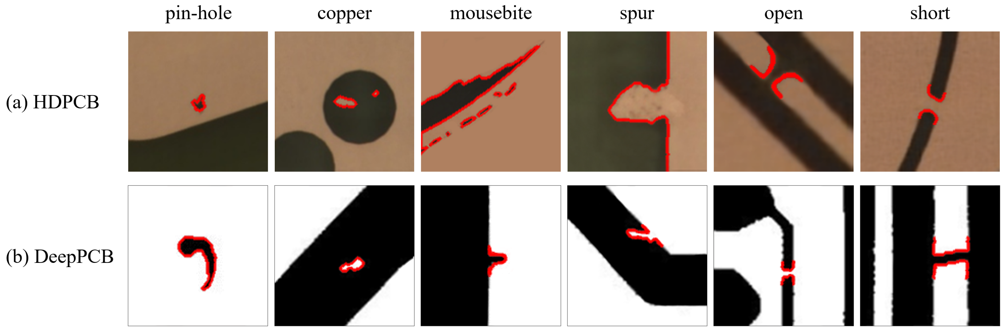
A way to achieve miniaturization and low power consumption in an electronics system is to use monolithic integration technology and flexible printed circuit board (PCB) technology. PCB is the carrier for the electrical interconnection of electronic components, the quality of which plays a significant role in sensors, magnetorquers, gyroscopes of microsystems and nano satellites. Thus, PCB defect detection is crucial for ensuring the safety performance and survival time of electronic systems. Their manufacturing process produces cosmetic and functional defects [1]. The latter may pose serious effects on the circuit’s performance. Thus, it is of significance to detect those defects for ensuring the reliability and safety of electronic products. The six major functional PCB defects, including pin-hole, copper, mousebite, spur, open circuit and short circuit, are presented in our HDPCB dataset as well as on the DeepPCB dataset [2], as shown in Figure 1. The red lines sketch the edge of defects, which are also the detection results of this work. Among the conventional PCB inspection methods, manual inspection is inefficient and prone to false detection, while contact-based electrical testing [3] may cause damage to the PCB. Thus, these methods have been replaced by non-contact automatic optical inspection (AOI) methods, which are based on images and use image processing algorithms to detect defects. We observe that functional defects can be regarded as shape or contour differences between the actual and the ideal circuit structure in images, resulting from the increase or decrease of copper material on PCB. Therefore, this work mainly aims at solving the defect localization problem using important image edge information.
Image-based methods can be mainly divided into two categories: non-reference methods and reference methods [1]. The latter can achieve more accurate defect detection but have strict requirements for image alignment. Non-reference methods, represented by deep learning methods [2,4,5,6,7], use algorithms such as the classic object detection [8,9,10] to directly detect defects by training a predictive model to learn the data distribution with a large number of positive or negative data. However, it faces challenges such as the few-shot problem, small object detection and poor interpretability, resulting from the diversity of defects and their unknown and subjective characteristics. Once the standard of defect changes, it needs to train the model again to adjust to the new conditions. Conversely, reference methods can achieve more accurate detection results with more prior information. They compare the test image with a template image to find differences and identify defects. The template image can be either a real defect-free image or a CAD design image. However, the effect of reference methods is highly dependent on image alignment. Thereby, strict image alignment is needed for high defect-detection accuracy.
The existing image-alignment methods can be generally categorized into pixel-based, frequency domain-based and feature-based. Among them, feature-based methods are more mature and widely used. They usually use Scale-Invariant Feature Transform (SIFT) [11], Speeded-Up Robust Features (SURF) [12], Oriented FAST and Rotated BRIEF (ORB) [13] to extract corner points, followed by feature matching and transform estimation. In this work, we use SURF for image alignment because it achieves higher accuracy than ORB while solving the drawbacks of high computational complexity and time consumption of SIFT. SURF finds the feature points by Hessian matrix polarization, then describes the feature points by Haar wavelet, calculates the main direction of the feature points and generates the feature description. It provides excellent performance, ensuring the accuracy of PCB defect detection later.
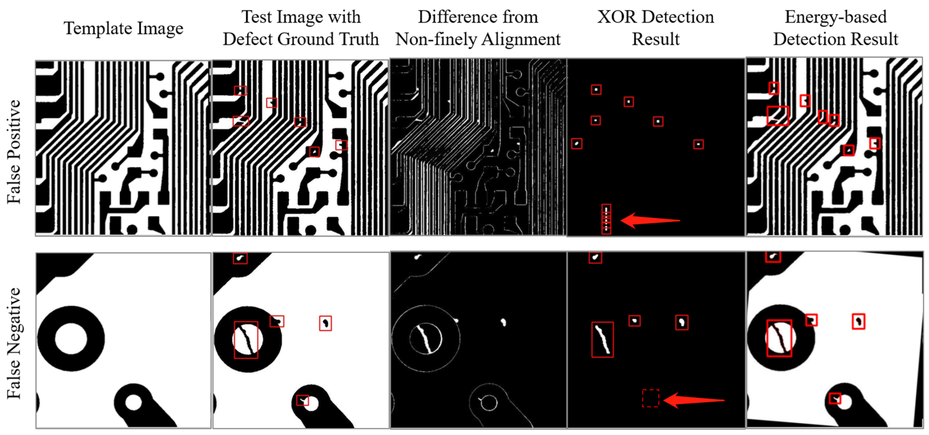
The existing reference-based defect-detection methods cannot address our high-resolution defect image problem well. Conventional defect-detection methods generally find the shape differences between the test image and the template image to locate PCB defects through image subtraction or exclusive OR (XOR) method. However, these methods rely on strict image alignment, making them vulnerable to the following conditions and having poor robustness: (1) images that are not strictly aligned, (2) subtle production deviations and (3) edge spurs caused by image segmentation. We found that the functional defects can all be represented as image contour anomalies.
Through observation and analysis, we found that PCB images have salient edge features. More importantly, functional defects can be viewed as contour anomalies, as presented in Figure 1. Specifically, they are reflected as either deviation in existing contours or contour increase or decrease. Therefore, studying how to use edge information effectively is not only more beneficial for detecting defects, but may also be able to solve the problems caused by edge spurs. However, there are few edge-guided defect-detection methods. An existing method compared the distance sequences of the edges through barycenter calculation and circular correlation to located defects, but the barycenter could easily be influenced by the defect contours, which decrease the detection accuracy.
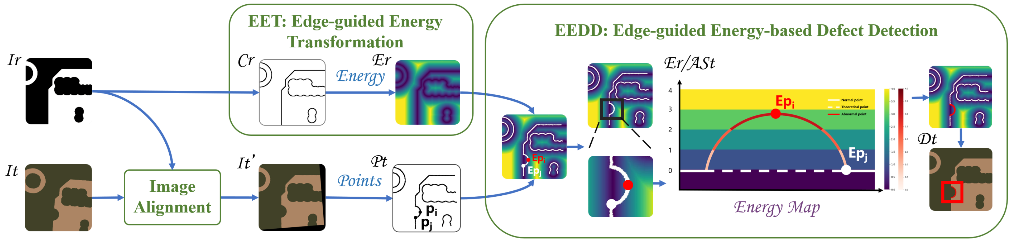
To leverage the valuable information of the edge, we propose to find an energy expression method to represent the energy of each pixel in the image for similarity measurement between template and test edges. The energy distribution, which we call Energy Map, is obtained from the template edge and then viewed as a standard to measure the error between the test edge and the template edge. It assigns an energy value to any point, where the energy is lowest at the edge and increases as further away from the edge. Thereby, when given any point of the test image, we can obtain its energy value relative to the template image to measure the similarity between the images. The higher the energy value of a point, the higher the anomaly score, and the higher the possibility of being judged as a defect. In this way, with the Energy Map, we can subtly achieve defect detection by measuring the anomaly energy values.
In this study, we propose an edge-guided energy-based high-precision PCB defect-detection method. Firstly, we propose an edge-guided energy transformation module (EET) to calculate the Energy Map of the template image. Secondly, we introduce SURF to align the test image and then sample edge points of the aligned test image. Thirdly, Energy Map is used to assign energy values to the aligned edge points through coordinate corresponding. In this way, the task is transformed into a point cloud energy measurement problem. In this way, we can use the inconsistency between the images, i.e., the energy anomaly region, for defect detection. Finally, we propose an edge-guided energy-based defect-detection module (EEDD) for defect localization. Specifically, the energy-based defect-detection method consists of the basic defect localization method, contour flood fill method and sliding-window contour flood fill method for defect contour refinement.
The proposed energy-based method addresses the challenges above well with the following advantages: the energy-based defect-detection method (1) addresses the problem of diversity and unknown numbers of defects without prior training, which relies on a large amount of annotated data, and in particular, excels in detecting tiny defects thanks to the pixel-by-pixel comparing and (2) is highly interpretable, enabling flexible adjustment of defect criteria according to different production needs, solving the problem of subjectivity in the definition of defects. In this way, it is more resistant to edge spurs and non-finely aligned images.
The main contributions are as follows:
  • We propose a novel edge-guided energy-based defect-detection framework, which introduces the Energy Map through energy transformation, and then transforms the functional defect-detection problem into a pixel-by-pixel edge point energy anomaly measurement problem;
  • We propose a novel edge-guided energy-based sliding-window contour flood fill method for robust defect contour refinement;
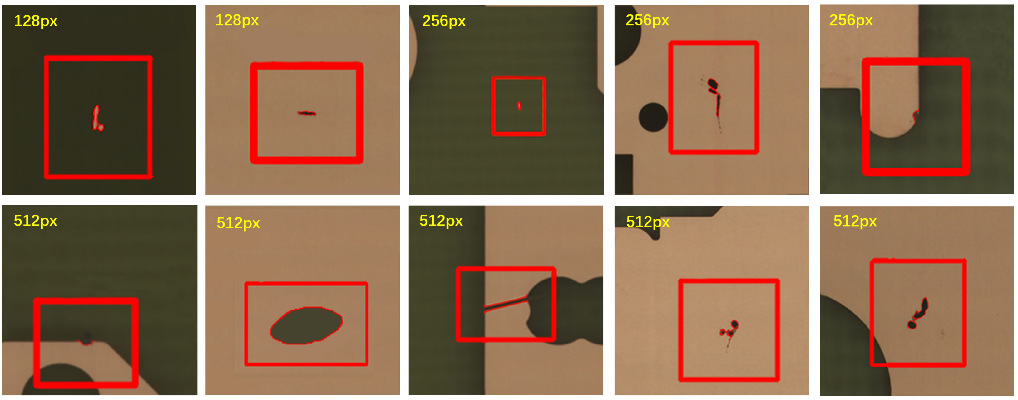
  • We made augmented synthetic DeepPCB-A datasets through geometric transformation which may cause non-finely aligned interferences for defect detection and realistic high-resolution HDPCB datasets containing multi-scale defects, and experiments verified the effectiveness and robustness of our method.

2. Related Work

Edge-guided Defect Detection. Conventional PCB detection methods are usually more interpretable in comparison to deep learning algorithms. They start by analyzing the causes and forms of defects theoretically, which can better meet the challenge of subjectivity in defect definition. At the feature-extraction level, conventional methods can be divided into three categories: texture-based, color-based and shape-based methods, which are more widely used since PCB images have distinct structural features. These methods commonly use algorithms such as morphological methods, edge detection [14], Hough transform [15] and Fourier shape descriptors to describe the boundary characteristics of objects. Most existing PCB defect-detection methods achieve defect localization through subtraction or XOR operations [1,16] to find out the shape differences between two images. By analyzing PCB functional defects, we found that they can be further regarded as anomalies of the edge. Unfortunately, we found that there is little research on edge-based defect detection. A method proposed to locate defects by finding the differences between the barycenter-edge points distance sequences of the template and test image using the circular correlation theorem. However, it [1,16] relies too heavily on the centroid calculation which can be easily influenced by defect contour points, leading to defect-detection errors and poor anti-interference ability.
Our proposed defect-detection algorithm based on edge-guided template Energy Map. In this way, we avoid the impact of defect contour points on the centroid calculation that leads to transmission errors, thus improving the accuracy and robustness and outperforming conventional methods.
Energy-based Measurement. In this paper, energy is a description of the image similarity, specifically, the error between edges. Distance is one of the effective evaluation metrics to express energy, with which we can easily achieve defect detection through energy measurement. The common distances includes Euclidean distance, Manhattan distance, Chamfer distance, Mahalanobis distance, cosine similarity, etc. Euclidean distance is the most common distance. It measures the straight-line distance between two points in space, which is simple and intuitive. Manhattan distance, also known as city block distance, is the distance between two points along the shortest path of a lattice-like network and is more applicable to path-planning problems. Chamfer distance calculates the distance from each point to its nearest neighbor, accumulates and averages these distances to measure the overall shape difference between two point clouds, which is widely used in point cloud matching, 3D reconstruction tasks. Mahalanobis distance is based on the covariance matrix, which considers the correlation between features and is more suitable for measuring the difference between high-dimensional data. Cosine similarity is used to measure the similarity between vectors by calculating the cosine of the angle between two vectors to measure the similarity between them and is suitable for similarity comparison of high-dimensional data.
In this paper, we focus on the distance between edge points of images. Therefore, Euclidean distance is more applicable to the case. Based on this, we introduce an Euclidean distance transform method, which uses the edge information of the template image to obtain the ideal energy distribution map of all points, thus avoiding the repeated distance calculation when detecting multiple defect images corresponding to the same template and greatly improving the efficiency of industrial detection.

3. Methods

We propose an edge-guided energy-based PCB defect-detection method and the overview is shown in Figure 2. The process begins with the input of the test image I t and a reference template CAD image I r . Then, the aligned test image I t is obtained through the Image Alignment module. Furthermore, segmentation and edge detection are used to obtain the test contour image and template contour images C r . C r is then used to calculate the Energy Map E r in the Energy Transformation module. Meanwhile, the test edge point cloud P t is sampled from the test contour image, and then each point can obtain an energy value from the template Energy Map through coordinate correspondence. Then, in the Energy-based Defect Detection module, the energy value of the target edge point is thresholded for defining anomalies. At this time, the energy value of the template Energy Map E r can be viewed as the anomaly score of the target edge point A S t , which can be used to compare the contour difference pixel by pixel to obtain the defect-localization result of test image D t .
This paper proposes a novel edge-guided energy-based PCB defect-detection method, encompassing three modules: Edge-guided Energy Transformation (in Section 3.1), Image Alignment and Edge-guided Energy-based Defect Detection (in Section 3.2). In the Image Alignment module, we use SURF since its better alignment performance in both accuracy and operation speed in the defect-detection task. The overview is shown in Figure 2.

3.1. Edge-Guided Energy Transformation

We propose an edge-guided energy transformation method (EET) to represent the energy distribution of points. Then, when given any point of the test image, we can obtain its energy value in the template image through coordinate position to measure the similarity.
We first extract the contours of the input images by semantic segmentation and edge detection [14], to distinguish all pixels into edge points and flat points. In particular, we found that using Euclidean distance transformation (EDT) [17], we can achieve the energy transformation subtly and quickly. The distance between any point and the nearest edge point in the template image is calculated through EDT, which we call Energy Map. In this map, any pixel is assigned an energy value. It is noteworthy that distance transformation is one way to represent the Energy Map, which can also be realized using other metrics or transformations. We define the edge points as e and the remaining flat points as p. Given the coordinate of any point, we can quickly and easily obtain the corresponding energy value with the Energy Map. The selection of the nearest edge point and the principle of calculating the energy value are shown in Figure 3. The energy at the edge is zero, as visualized darkest in the image. With increasing distance from the edge, the energy gradually increases and becomes brighter.
Here, we use the Euclidean distance transformation method to calculate the energy value of the arbitrary point. First, we review the one-dimensional distance conversion method. Let G be a one-dimensional grid and f : G R be the grid sampling function. We define the one-dimensional distance transformation of f as D f : G R . In this work, the Euclidean distance is utilized as the metric between edge points e and flat points p, denoted as d ( e , p ) . The distance transformation aims to find the nearest edge point for any flat point, assigning the flat one an energy value, which is represented by a function f ( e ) , and then we calculate the distance D f ( p ) from the flat point p to the corresponding nearest edge point e. The Euclidean distance transformation of f is calculated as Equation (1).
D f ( p ) = min p G ( d ( e , p ) + f ( e ) )
In this paper, we use two-dimensional distance between a flat ( x , y ) point to the nearest edge point ( x , y ) to express the its energy. Then we calculate the two-dimensional distance transform for our edge images under the squared Euclidean distance by Equation (2).
D f ( x , y ) = min x , y x x 2 + y y 2 + f x , y
Since the distance relationship between the two dimensions x and y is independent of an image. Therefore, we can obtain the distance transform of the two-dimensional distance transform by first calculating the one-dimensional distance transform of each column of the grid D f | x ( y ) by Equation (1) and then calculating the one-dimensional distance transform of each row based on that. In this way, Equation (2) can be rewritten as Equation (3).
D f ( x , y ) = min x x x 2 + D f x ( y )
where D f | x ( y ) ) is a one-dimensional distance transform of f restricted to the column indexed by x. Thus, the Energy Map, i.e., the distance distribution map, can be obtained by calculating Equation (4).
E = min x x x 2 + D f x ( y )
here, the Energy Map E of the template image is derived, which is a significant reference for subsequent defect-detection tasks.

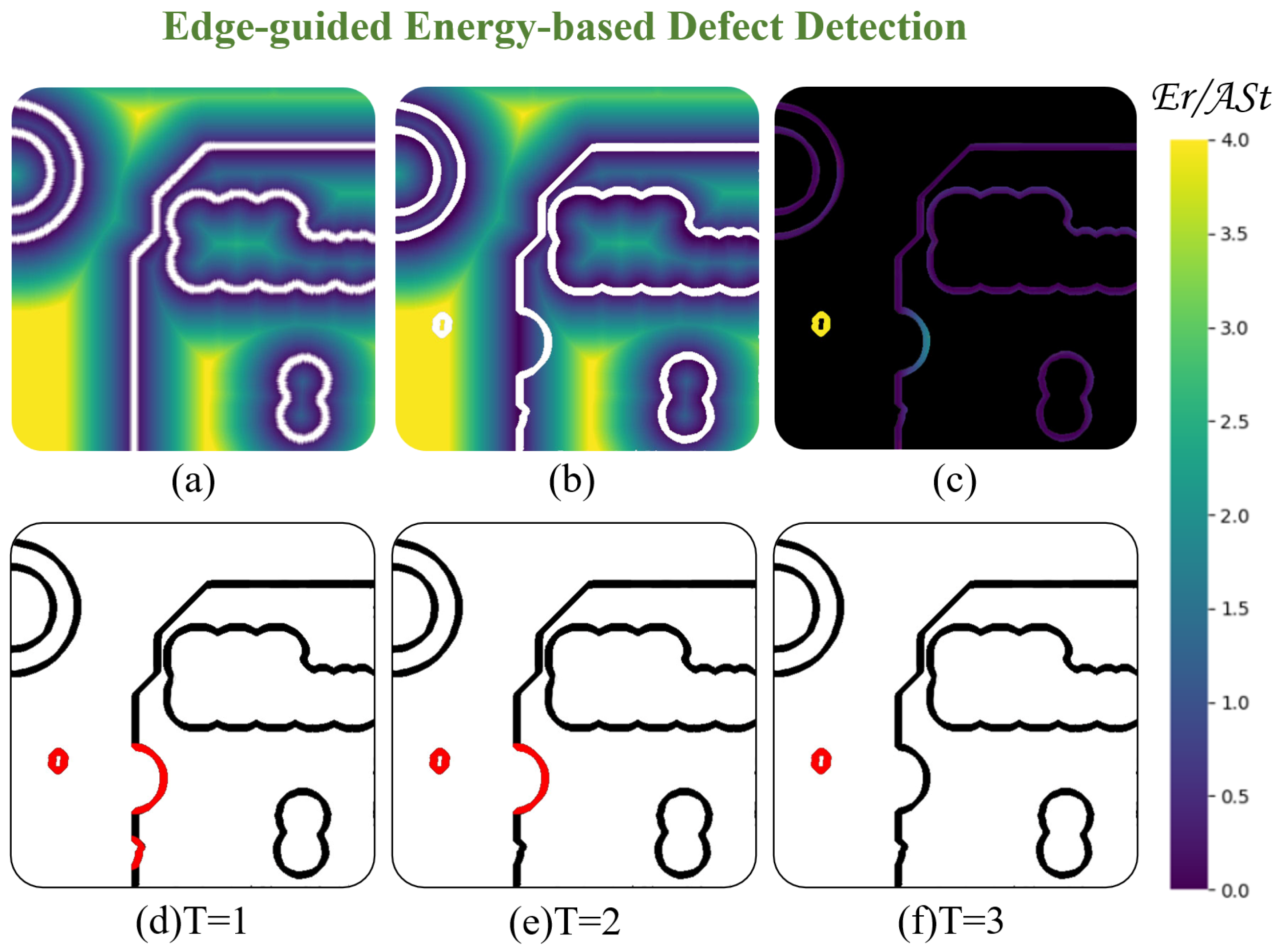
3.2. Edge-Guided Energy-Based Defect Detection

A segment consisting of all adjacent defective points in a contour is called a defective segment S a . We first propose a novel edge-guided energy-based defect localization method to find out the fragments S n S a by defining an adjustable threshold in Section 3.2.1. All the energy values of points in the S n exceed the threshold. We do this to solve the problem resulting from the images not being finely aligned. However, it results in a new problem that the defect fragments S n S a may be not the incomplete defect contour. Therefore, we further propose a novel edge-guided energy-based contour flood fill method that enables us to obtain S a through S n according to the continuity of edge defects in Section 3.2.2.

3.2.1. Edge-Guided Energy-Based Defect Localization

We found that the functional defects, such as pinhole, copper, mousebite, spur, open circuit, short circuit and other deviations, have distinct edge features, which can be regarded as differences between the target and template contour. To take advantage of this characteristic, this paper proposes an edge-guided energy-based defect-detection method (EEDD) based on the energy-based alignment result. The method transforms functional defects localization into a point cloud energy anomaly measuring problem by energy thresholding.
The innovation of our algorithm is using the energy measuring method to replace the conventional subtraction and exclusive OR (XOR) detection method. The core concept is depicted in Figure 4. We propose to further localize the defects based on the energy values of the transformed point cloud obtained from the energy-based alignment outcome, where most energy values have been decreased to zero. By defining a threshold value to confirm whether a point belongs to a defect, the energy value in the template Energy Map E r can be considered to be the anomaly score of the target contour point A S t . The higher the energy value of a point, the higher the abnormal score, and the higher the possibility of being judged as a defect. If the anomaly score exceeds a certain value or falls within a specific range according to a specific standard, the pixel can be considered one point of a defect. The proposed method is highly interpretable, as shown in Figure 4. By adjusting the energy threshold T, it is easy and flexible to fine-tune and adjust different industrial standards and production requirements. Setting threshold value enables our approach to overcome issues such as image misalignment or edge spur resulting from the production process or image pre-processing, and finally achieve higher accuracy and stronger robustness.

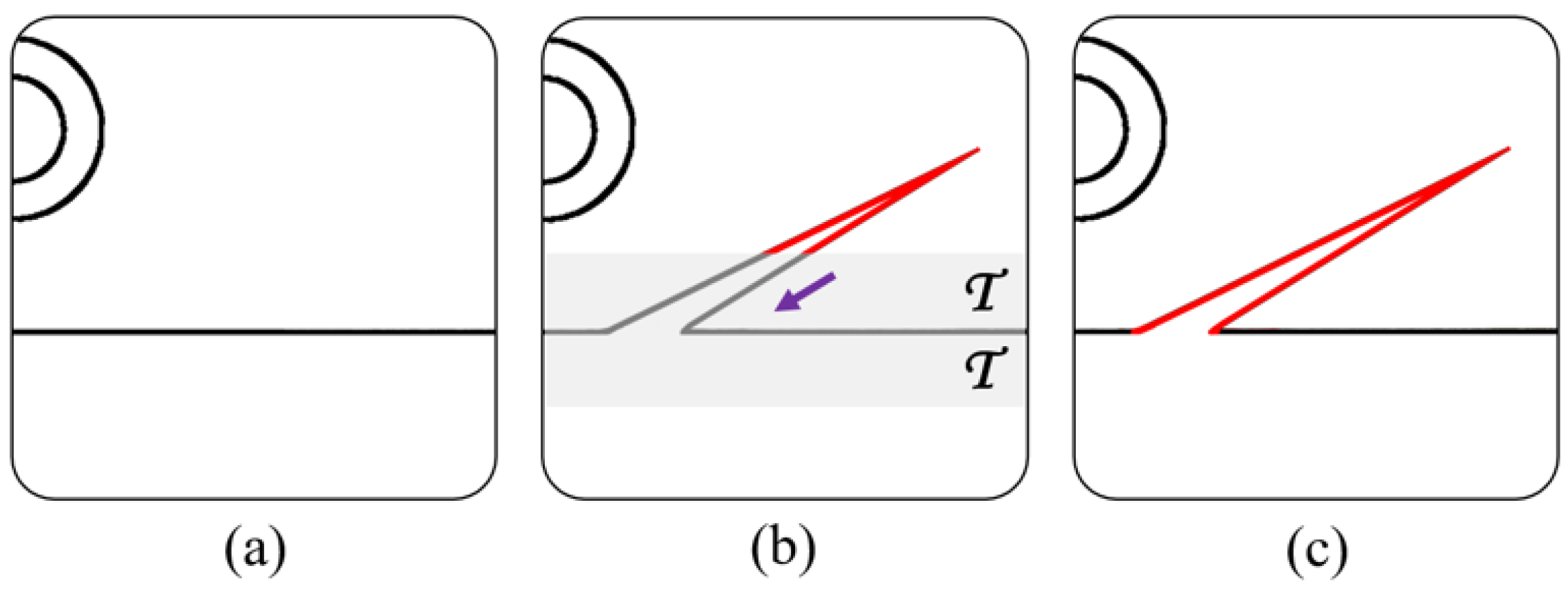
3.2.2. Edge-Guided Energy-Based Contour Flood Fill Method for Defect Refinement

We obtain a subset of the complete defect contour points, the energy values of which are greater than a threshold T by the energy-based defect localization method in Section 3.2.1, as shown in Figure 5b.
The principle of the proposed edge flood fill method is as follows. The point with the highest energy on the defect fragment S n is taken as the starting point, i.e., the seed point, and then backtrack along the contour to both ends. During the backtracking process, the energy value of the flooding point, i.e., the growing point, is expected to decrease gradually until it no longer decreases. At that point, we obtain the complete defect fragment S a , as shown in Figure 5c. Our proposed one-dimensional flooding method is expressed by Equation (5).
P n = 1 , E n < E n 1 0 , E n = E n 1
where P n denotes the probability of the current contour point n that is included in the defect fragment. When the energy value of the current contour point E n is less than that of the previous contour point E n 1 , it indicates that the current point n is a defect point, i.e., the probability is 1. When the energy of the current contour point E n is equal to the energy of the previous contour point E n 1 , it means that the current point is not a defect point, i.e., the probability is 0.
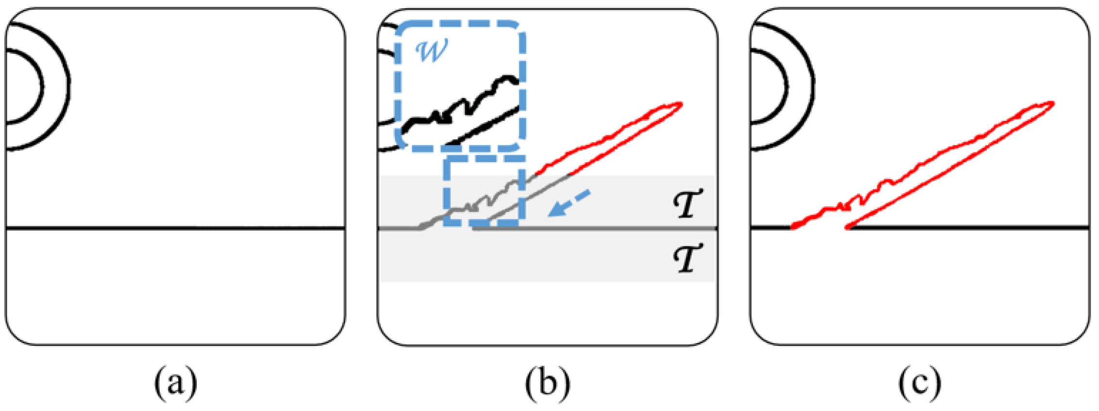
However, in practice, defects are often irregular. The overall change trend of energy during defect contour retracing is decreasing, but the energy between consecutive points is not strictly monotonically varying; it may fall and rise at times. Therefore, we propose the concept of a sliding window, as shown in Figure 6b. If the overall trend is decreasing within a window, the flooding operation is continued until it tends to be stable. Then finally we obtain the complete defect contour, as shown in Figure 6c.
If the energy of the current point E n in the flooding process is lower than the energy value of a point E n s that occurs before a step length s along the traceback path, we could consider the energy trend is still decreased. In this way, the current point is considered a defective point, i.e., its probability P n of being judged as defective is 1, which can be expressed as Equation (6).
P n = 1 , E n < E n s 0 , E n E n s

4. Experiments

4.1. Datasets

4.1.1. DeepPCB Dataset

To simulate the real image acquisition situation, we performed geometrically transformed image enhancement on the existing paired DeepPCB dataset. Our proposed method was evaluated by measuring the defect-detection metrics to compare the effectiveness of the proposed method with several conventional alignment methods and detection methods.
The DeepPCB dataset [2] consists of 1500 pairs of 640 × 640 PCB images containing six types of defects, such as pinhole, copper, mousebite, spur, open and short, as can be seen in Figure 1. Each pair includes a defect-free template image and a defective test image with approximately 3 to 12 defects. We made the DeepPCB-A dataset by augmenting the 500 image pairs in the test set divided by the original authors with a random geometric transformation. We randomly rotated and translated 480 images, and the remaining 20 images were selected for translation only. The details are shown in Table 1, where t x , t y indicate the horizontal and vertical offset of the image, respectively. We randomly selected a possible minor translation within 2 percent of image size and rotation angle between 2 to 5 degrees on the original test image x R W × H to obtain the transformed image x . Then we performed a central crop on the paired template image, test image and enhanced test image. Then we obtained 512 × 512 template images X T e m p l a t e , test images X T e s t and transformed test images X T e s t , respectively, with approximately 3 to 10 defects retained in each pair. We altered the ground truth of the bounding boxes of defects correspondingly. To evaluate defect localization rather than classification, we used the F1-score [18] of a single category of defect detection in the experiments.

4.1.2. HDPCB Dataset

We presented the HDPCB dataset comprising a billion-pixel high-resolution paired PCB template and test images covering 100 PCB patterns. The weight and height of the images are about 8300 px and 26,000 px, which produce the following characteristics of the dataset: Firstly, different PCB patterns may consist of multi-scale sub-units, which cause the varying numbers of sub-units, i.e., the massive repetitive features in a high-resolution image. That may cause some problem for the commonly used feature-based image alignment methods and, once the images are not finely aligned, the reference-based defect-detection methods would not perform well. Secondly, our data are RGB images, and image segmentation is needed to further obtain the edge information, which may cause some edge spurs. Moreover, the production errors are common. That could cause a subtle offset between different test images and the standard images around the edge region. Thirdly, high resolution increases the possibility of multi-scale defects, varying from a few pixels to several hundred pixels, which poses certain challenges to detection for some defect-detection methods. Last but not least, unlike the manually created synthetic DeepPCB dataset, our realistic HDPCB dataset contains rich styles of defects. They may be more irregular and some of them may be similar with some defect-free PCB elements.

4.2. Results on DeepPCB-A Dataset

Reference-based defect-detection methods have strict requirements for alignment accuracy. Using test images that are not precisely aligned for detection can easily lead to false or missed results. In this section, we designed ablation experiments on the alignment and detection methods. The objects were the aligned images on the Test x–Test x dataset using multiple alignment methods. We evaluated our proposed energy-based detection method, compared with conventional methods based on morphology and subtraction. The experiments aim to compare the performance of different alignment methods, and more importantly, to compare the performance of our detection method with the conventional subtraction or XOR method.
The effectiveness of object detection is commonly evaluated by the mean average precision (mAP) [19]. A detection result is considered correct if the intersection over union (IoU) between the predicted bounding box and ground true (GT) with the same class is greater than 0.33. In this work, we compared the performances of the final defect detection by calculating the F1-score, the harmonic mean of Precision and Recall, to evaluate the ability of different image alignment and defect-detection methods.
We validated the alignment and defect-detection results on the DeepPCB-A defect annotation dataset. The experiment results are shown in Table 2. On the one hand, the results also revealed that SIFT and SURF methods achieved greater alignment effects than ORB in the PCB defect task. In the condition of the conventional detection method, SURF showed a slight disadvantage against SIFT but was greater in the condition of our energy-based detection. On the other hand, as can be seen in the table, the F1-scores of the energy-based method considerably surpassed those of the subtraction or XOR detection methods when using the same alignment algorithm. The results indicated that our defect-detection method approach achieved remarkable performance compared to the conventional detection methods.
Two sets of images were chosen to compare the performance of XOR and our method, as depicted in Figure 7. There are issues such as not being strictly aligned and edge spurs resulting from segmentation. To reduce interference from these issues, the XOR method needed to apply morphological techniques such as opening and closing operations. The opening operation removed isolated dots, burrs and thin connecting lines between two shapes. The closing operation filled in small holes and bridged small cracks. As shown in Figure 7, most of the interferences have been eliminated in the XOR-processed image. Nevertheless, the choice of a smaller kernel matrix to avoid damaging the original image’s structure resulted in False Positives caused by some uneliminated edge interference (Figure 7 top). Conversely, choosing a larger kernel matrix to eliminate interferences such as edges and tiny holes wrongly removed tiny defects, i.e., False Negatives (Figure 7 bottom). Our method, in contrast, handled the above challenges with high robustness. For instance, it avoided the breakdown of small defects since it did not rely on morphological processing.

4.3. Results on HDPCB Dataset

In this section we first compared the inspection results on our HDPCB dataset with those of one of the most widely used PCB optical inspection equipment manufacturers based on optical technology and machine vision for quality inspection in the Chinese industry (in the paper we named it YM). Due to their closed-source algorithm, we compared the results on the limited 35 PCB billion-pixel images containing 74 sets of functional defects that we were able to obtain. Unlike the evaluation metrics used on the DeepPCB-A synthetic dataset (Section 4.2), industry is more concerned with the number of defects correctly detected, false detections and missing detections, i.e., True Positive, False Positive and False Negative, respectively. The results are shown in Table 3. The high-resolution images allow the PCB defects varying from multi-scale to rich styles, which increase the difficulty for other detection method that may result in many False Positives and False Negatives. As can be seen in the table, our method achieved higher precision and more robust effectiveness.
Moreover, we conducted extensive experiments on our entire HDPCB dataset using the proposed energy-based detection method. Our method achieved high-precision pixel-by-pixel defect localization results, as shown in Figure 8. Experiments indicated that our approach is accurate and efficient in detecting defects of multiple scales and morphologies in billion-pixel images. These results demonstrated our advantages over conventional methods and deep learning algorithms. On the one hand, the experiments revealed the superiority of our proposed alignment method over conventional subtraction or XOR detection methods, which is robust against the non-finely aligned images, edge spurs and performs well in detecting tiny defect. On the other hand, the efficient performance of our detection algorithm surpassed deep learning methods, and the reasons were as follows: Firstly, our algorithm could achieve outstanding detection outcomes without prior training or a large number of annotated data. Secondly, our algorithm performed better for tiny defect-detection tasks of high-resolution images, as it processed detection directly on high-resolution images without pixel compression, preventing the loss of detail and missed detection of fine defects. Additionally, it could avoid inefficient, repetitive detection of large-scale defects due to sliding window slicing of high-resolution images.

5. Discussion

The energy-based defect-detection method proposed in this paper effectively solves the detection problem in the case of imprecise alignment that cannot be solved by conventional subtraction or exclusive OR algorithms. However, the present method also has some limitations. For example, we define a small threshold to ensure a certain seat belt around the edge region in order to solve the above problem, which causes some kind of tiny defects with very low energy within the seat belt to be difficult to detect. Furthermore, experiments on the X T e m p l a t e X T e s t data, that we did not show in this paper because of the poor performances, indicated that the existing feature-based alignment method including SIFT and SURF can not address the problem due to the defect feature interference, especially in DeepPCB-A dataset and repetitive feature resulting from the high-resolution images in our HDPCB dataset. Therefore, improving the precision of the alignment algorithm for reference-based detection approaches is also a researchable direction in the future to improve the defect-detection accuracy of this method.

6. Conclusions

This study proposes an edge-guided energy-based PCB defect-detection approach for ensuring the safety performance and the survival time of electronics in more than just the space industry. The novelty of this work is to transform the defect-detection task into a target edge point cloud energy measurement problem through energy transformation. The difference between the target contour and the template contour point cloud is highlighted, and the defect is localized by measuring the energy value of the target contour point cloud. Experiments on the 512 × 512 synthetic DeepPCB-A dataset showed that, when using the same alignment methods, the F1-score results of our proposed energy method reached at least 5 percentage points higher than the conventional PCB defect-detection method, and the comparison with the widely used PCB optical inspection equipment manufacturer in industry on our realistic billion-pixel HDPCB dataset showed that our method had higher accuracy and fewer false detections. Experiments demonstrated that the proposed edge-guided energy-based defect-detection method is more robust to edge spurs, poorly aligned images and multi-scale defects, varying from several pixels to hundreds of pixels. Furthermore, it is more interpretable and adaptable to production needs as it can flexibly adjust anomaly thresholds to adapt different defect criteria to production needs. Above all, the proposed energy-based method is applicable not only to PCB inspection but also to other surface defect-detection problems with distinct structural features.

Author Contributions

Conceptualization, S.D., L.D.; methodology, S.D., L.D.; software, S.D., L.D.; validation, S.D., L.D., H.H.; formal analysis, S.D.; investigation, S.D., L.D., H.H., Y.X., J.X., X.C.; resources, T.S., S.Y., B.C., L.D., L.W., L.L., S.X., Y.L. (Yuan Li), Y.L. (Yizheng Li); funding acquisition, T.S., B.C.; data curation, S.D., L.D., L.W., S.Y., H.H., Y.F., X.T., R.S., L.L., S.X., Y.L. (Yuan Li), Y.L. (Yizheng Li); writing—original draft preparation, S.D.; writing—review and editing, S.D., L.D., T.S., B.C., Y.X., H.Y., J.X.; visualization, S.D., L.D., T.S., B.C., Y.X., H.Y., J.X.; supervision, S.D., L.D., T.S., S.Y., B.C.; project administration, S.D., L.D., T.S., S.Y., B.C. All authors have read and agreed to the published version of the manuscript.

Funding

This research was funded by Optoelectronic Measurement and Intelligent Perception Zhongguancun Open Lab., and Space Optoelectronic Measurement and Perception Lab., Beijing Institute of Control Engineering (No.LabSOMP-2022-02). This work was also supported by the National Key Research and Development Program of China under Grant 2020AAA0108302. The APC was funded by Optoelectronic Measurement and Intelligent Perception Zhongguancun Open Lab., and Space Optoelectronic Measurement and Perception Lab., Beijing Institute of Control Engineering (No.LabSOMP-2022-02) and the National Key Research and Development Program of China under Grant 2020AAA0108302.

Acknowledgments

This work was supported by the IoT Intelligent Microsystem Center of Tsinghua University-China Mobile Joint Research Institute.

Conflicts of Interest

The authors declare no conflict of interest.

References

  1. Moganti, M.; Ercal, F.; Dagli, C.H.; Shou, T. Automatic PCB Inspection Algorithms: A Survey. Comput. Vis. Image Underst. 1996, 63, 287–313. [Google Scholar] [CrossRef]
  2. He, F.; Tang, S.; Mehrkanoon, S.; Huang, X.; Yang, J. A Real-time PCB Defect Detector Based on Supervised and Semi-supervised Learning. In Proceedings of the European Symposium on Artificial Neural Networks, Bruges, Belgium, 2–4 October 2020. [Google Scholar]
  3. Widianto, W.; Yotsuyanagi, H.; Ono, A.; Takagi, M.; Roth, Z.; Hashizume, M. A built-in electrical test circuit for interconnect tests in assembled PCBs. In Proceedings of the 2012 2nd IEEE CPMT Symposium Japan, Kyoto, Japan, 10–12 December 2012; pp. 1–4. [Google Scholar]
  4. Ding, R.; Dai, L.; Li, G.; Liu, H. TDD-net: A tiny defect detection network for printed circuit boards. CAAI Trans. Intell. Technol. 2019, 4, 110–116. [Google Scholar] [CrossRef]
  5. Hu, B.; Wang, J. Detection of PCB Surface Defects With Improved Faster-RCNN and Feature Pyramid Network. IEEE Access 2020, 8, 108335–108345. [Google Scholar] [CrossRef]
  6. Li, Y.T.; Kuo, P.; Guo, J.I. Automatic Industry PCB Board DIP Process Defect Detection with Deep Ensemble Method. In Proceedings of the 2020 IEEE 29th International Symposium on Industrial Electronics (ISIE), Delft, The Netherlands, 17–19 June 2020; pp. 453–459. [Google Scholar]
  7. Tsai, D.M.; Chou, Y.H. Fast and Precise Positioning in PCBs Using Deep Neural Network Regression. IEEE Trans. Instrum. Meas. 2020, 69, 4692–4701. [Google Scholar] [CrossRef]
  8. Girshick, R.B.; Donahue, J.; Darrell, T.; Malik, J. Rich Feature Hierarchies for Accurate Object Detection and Semantic Segmentation. In Proceedings of the 2014 IEEE Conference on Computer Vision and Pattern Recognition, Columbus, OH, USA, 24–27 June 2014; pp. 580–587. [Google Scholar]
  9. Ren, S.; He, K.; Girshick, R.B.; Sun, J. Faster R-CNN: Towards Real-Time Object Detection with Region Proposal Networks. IEEE Trans. Pattern Anal. Mach. Intell. 2015, 39, 1137–1149. [Google Scholar] [CrossRef] [PubMed]
  10. Redmon, J.; Divvala, S.K.; Girshick, R.B.; Farhadi, A. You Only Look Once: Unified, Real-Time Object Detection. In Proceedings of the 2016 IEEE Conference on Computer Vision and Pattern Recognition (CVPR), Las Vegas, NV, USA, 27–30 June 2016; pp. 779–788. [Google Scholar]
  11. Lowe, D. Distinctive image features from scale-invariant key points. Int. J. Comput. Vis. 2003, 20, 91–110. [Google Scholar]
  12. Bay, H.; Tuytelaars, T.; Gool, L.V. SURF: Speeded up robust features. In Proceedings of the 9th European conference on Computer Vision—Volume Part I, Graz, Austria, 7–13 May 2006. [Google Scholar]
  13. Rublee, E.; Rabaud, V.; Konolige, K.; Bradski, G. ORB: An efficient alternative to SIFT or SURF. In Proceedings of the 2011 International Conference on Computer Vision, Barcelona, Spain, 6–13 November 2011; pp. 2564–2571. [Google Scholar] [CrossRef]
  14. Canny, J. A Computational Approach to Edge Detection. IEEE Trans. Pattern Anal. Mach. Intell. 1986, PAMI-8, 679–698. [Google Scholar] [CrossRef]
  15. Duda, R.O.; Hart, P.E. Use of the Hough transformation to detect lines and curves in pictures. Commun. ACM 1972, 15, 11–15. [Google Scholar] [CrossRef]
  16. Onshaunjit, J.; Srinonchat, J. Algorithmic Scheme for Concurrent Detection and Classification of Printed Circuit Board Defects. Comput. Mater. Contin. 2022, 71, 355–367. [Google Scholar] [CrossRef]
  17. Felzenszwalb, P.F.; Huttenlocher, D.P. Distance Transforms of Sampled Functions. Theory Comput. 2012, 8, 415–428. [Google Scholar] [CrossRef]
  18. Chinchor, N.; Sundheim, B.M. MUC-5 evaluation metrics. In Proceedings of the Fifth Message Understanding Conference (MUC-5), Baltimore, MD, USA, 25–27 August 1993. [Google Scholar]
  19. Everingham, M.; Van Gool, L.; Williams, C.K.; Winn, J.; Zisserman, A. The pascal visual object classes (VOC) challenge. Int. J. Comput. Vis. 2010, 88, 303–338. [Google Scholar] [CrossRef]
Figure 1. Main types of functional defects on our realistic high-resolution HDPCB dataset (copper in brown and board in dark green) and synthetic DeepPCB dataset (copper in white and board in black). The detection results of our energy-based method sketch the contours of defects in red.
Electronics 12 02306 g001
Figure 2. Overview of the edge-guided energy-based PCB defect-detection method, including edge-guided energy transformation module (EET), image alignment module and edge-guided energy-based defect-detection module (EEDD).
Electronics 12 02306 g002
Figure 3. Illustration of Energy Map calculation principle. (a) Template contour. (b) Template Energy Map. (c) A local image of (b). Let the upper left corner of (c) be the coordinate origin. (c) shows the selection of the nearest contour point corresponding to the point (0, 0) with coordinates and the principle of calculating the energy value. The further away from the edge, the higher the energy value, which is brighter as visualized.
Electronics 12 02306 g003
Figure 4. Illustration of the edge-guided energy-based defect-detection method. (a,b) show the overlay effect of the template and the target edge on the template Energy Map, respectively. (c) shows the visualization of the energy values of the target edge points. (df) show the different defect-detection results with different threshold values.
Electronics 12 02306 g004
Figure 5. Illustration of the edge-guided energy-based contour flood fill method. (a) Template contour. (b) Localization results in a defect contour. T denotes the threshold for the energy-based detection method. Arrow indicates the direction of flooding. (c) The result of the energy-based contour flood fill method.
Electronics 12 02306 g005
Figure 6. Illustration of the edge-guided energy-based sliding-window contour flood fill method. (a) Template contour. (b) Localization results in a defect contour. T denotes the threshold for the energy-based detection method. Arrow indicates the direction of flooding. W is a sliding window, in which although the energy between consecutive points is not strictly monotonically varying but the overall change trend of energy is decreasing along the direction of flooding. (c) The refined result of the energy-based contour flood fill method with sliding window.
Electronics 12 02306 g006
Figure 7. Comparison of the effectiveness of different methods on DeepPCB-A dataset. (top) False Positives in XOR method resulting from non-fine alignment or edge spur. (bottom) False Negatives in XOR method due to the missing detect of tiny defect.
Electronics 12 02306 g007
Figure 8. Multi-scale and different types of PCB defect-detection results on our HDPCB dataset. Our method outlines the defect segment in red and the size of each image is marked in yellow.
Electronics 12 02306 g008
Table 1. Transformation details and composition of 500 augmented images of DeepPCB (DeepPCB-A) dataset, 4% for random translation (t) only and 96% for rotation (R) and translation.
TransformationTransformation DetailsDeepPCB-A Composition
t( t x ± 0.02*W, t y ± 0.02*H)20 (4%)
R & t ±2° < R < ± 5°, ( t x ± 0.02*W, t y ± 0.02*H)480 (96%)
Table 2. F1-score results of defect-detection evaluation ablation experiments using different alignment- and defect-detection methods on the DeepPCB-A dataset.
DetectionSubtraction/XOR [16]Energy-Based
Alignment
ORB [13]75.191.0
SIFT [11]86.292.1
SURF [12]85.592.3
Table 3. Comparison of results of our method and a PCB inspection equipment manufacturer (YM) on the HDPCB dataset that contains 74 sets of functional defects in total.
Truth and Prediction SituationYMEnergy-Based
True Positive970
False Positive2613
False Negative654
Disclaimer/Publisher’s Note: The statements, opinions and data contained in all publications are solely those of the individual author(s) and contributor(s) and not of MDPI and/or the editor(s). MDPI and/or the editor(s) disclaim responsibility for any injury to people or property resulting from any ideas, methods, instructions or products referred to in the content.

