Article

Design of a Low-Profile Wideband Magnetoelectric Dipole Antenna with Reduced Gain Drop

College of Electronics and Information Engineering, Sichuan University, Chengdu 610065, China
*
Author to whom correspondence should be addressed.
Electronics 2022, 11(7), 1156; https://doi.org/10.3390/electronics11071156
Submission received: 20 February 2022 / Revised: 4 March 2022 / Accepted: 4 March 2022 / Published: 6 April 2022
(This article belongs to the Topic Antennas)

Abstract

:
In this paper, a novel low-profile magnetoelectric (ME) dipole antenna with wideband is presented. The conventional vertical fixing structure is bended four times from the center to the sides. The Γ-shaped feeding structure is bended two times to lower the height of the antenna step by step. The effect of three kinds of vertical wall is discussed to show their influence on boresight gain. Through comparison, only one vertical wall is erected on the left side of the ground to decrease the boresight gain drop at 2.2 GHz. Both simulation and analysis are made to sufficiently explain the working principle. At last, the proposed ME dipole antenna has only 0.095λ00 is the center operating wavelength in free space) in height, and the wideband property is still maintained. By simulation, the relative bandwidth for VSWR < 2.0 is 47.9% (from 1.35 to 2.2 GHz). The boresight gain ranges from 8.1 to 9.6 dBi in the operating band. The measured relative bandwidth for VSWR < 2.0 is 50.3% (from 1.34 to 2.24 GHz), and the boresight gain ranges from 7.38 to 8.73 dBi. The gain drop on boresight is less than 1.4 dBi. Radiation patterns show a unidirectional characteristic in the whole operating band. Additionally, the cross-polarization level is less than −25 dB on boresight. The simulating and measuring results agree well with each other. Therefore, the proposed antenna is suitable for applications of limited height and wideband.

1. Introduction

To meet the increasing requirement of wireless communication systems, wideband equipment is widely designed and produced by suppliers. Traditional narrow band antennas are no longer suitable for current wideband and ultra-wideband (UWB) wireless applications [1]. Conventionally, two methods are adopted to satisfied the wideband communication: the first one is to use multiple narrow band antennas that worked at a continuous frequency band to realize a wideband operation. The second one is to design a wideband antenna to cover the whole operating band. For the first method, the multiple antennas will occupy much installation space, and lots of cables will be needed to connect to the input port of each antenna element. This inevitably increases the complexity of the whole system. Therefore, to adopt a wideband antenna to realize the wideband communication is feasible and rational.
To save the installation space and decrease the wind drag, a low-profile antenna is widely adopted in lot of scenarios, such as the surface of aircraft, vessel, building, and so on. Up until now, lots of low-profile antennas were designed in the literature. In [2], an ultralow-profile patch antenna was designed with only 0.01λ0 in height by using the slot-loading technique. In [3,4,5], three kinds of metamaterial loaded methods were adopted to realize a low profile. In [6], a filter antenna has a profile of 0.026λ0 but with single-frequency point operation. Recently, a multimode technique was taken to broaden the bandwidth of a low-profile antenna. In [7], with a profile of 0.07λ0, three modes (TM10, TM12, and antiphase TM22) were excited simultaneously to realize a relative bandwidth of 26.2% for S11 < −15 dB. In [8], based on multiple mode partial aperture, a microstrip antenna is able to work at the bandwidth of 57.3% with a profile of 0.044λ0.
In recent years, the ME dipole antenna, which was first proposed by Alvin Chlavin [9] and developed by Luk [10], has attracted lots of research. This kind of antenna has the advantages of wideband, stable unidirectional radiation, low front–back ratio, and equal E and H planes [11,12,13,14]. To reduce the profile of the ME dipole, many methods were proposed in the literature [15,16,17,18,19]. In [15], the author utilized an obtuse triangular structure to reduce the antenna thickness to 0.097λ0, and an impedance bandwidth of 28.2% was achieved. In [16], by using a pair of vertically oriented folded shorted patches, the antenna height is reduced from 0.25λ0 to 0.116λ0. In [19], the magnetic dipole mode of ME dipole antenna was formed by the slot-aperture between patches. Therefore, the height of the antenna can be as low as 0.11λ0, and the impedance bandwidth is 27.6% for S11 < −15 dB.
In this paper, a novel wideband low-profile ME dipole antenna is presented. To decrease the height of the traditional ME dipole, a multi-bending technique is introduced. Both the fixing structure and Γ-shaped feeding structure are bended to lower the profile step by step. Additionally, the effect of three kinds of vertical wall is discussed, and only one vertical wall is erected on the left side of the ground to avoid the gain drop on boresight at last. Finally, the total height of the proposed ME dipole antenna is only 0.095λ0, and the measured relative bandwidth is up to 50.3%.

2. Technique and Geometry

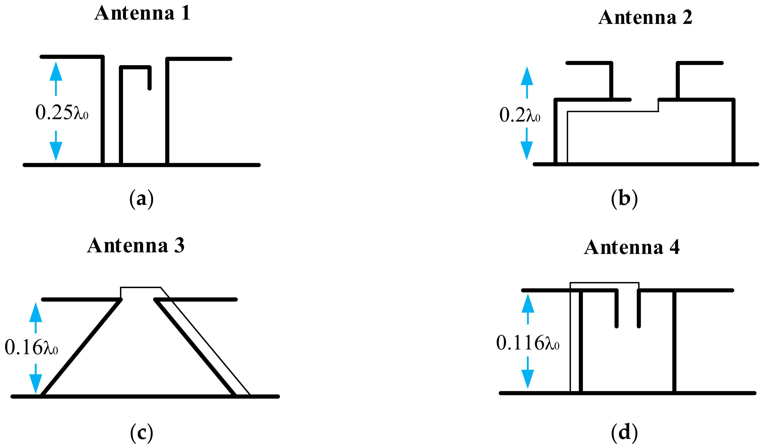
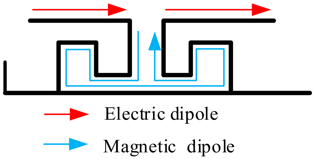
2.1. Low-Profile Technique

Ahead of this design, four kinds of ME dipole antennas are depicted in Figure 1 to show the current low-profile technique [15]. Antenna 1 is the traditional ME dipole with a profile of 0.25λ0. For antenna 2, the vertical fixing structure is bended and the height can be lowered to 0.2λ0. For antenna 3, an obtuse-triangular structure is introduced to lower the antenna height to 0.16λ0. For antenna 4, the feeding line is moved to the outside of the fixing structure, and the final height is 0.116λ0.

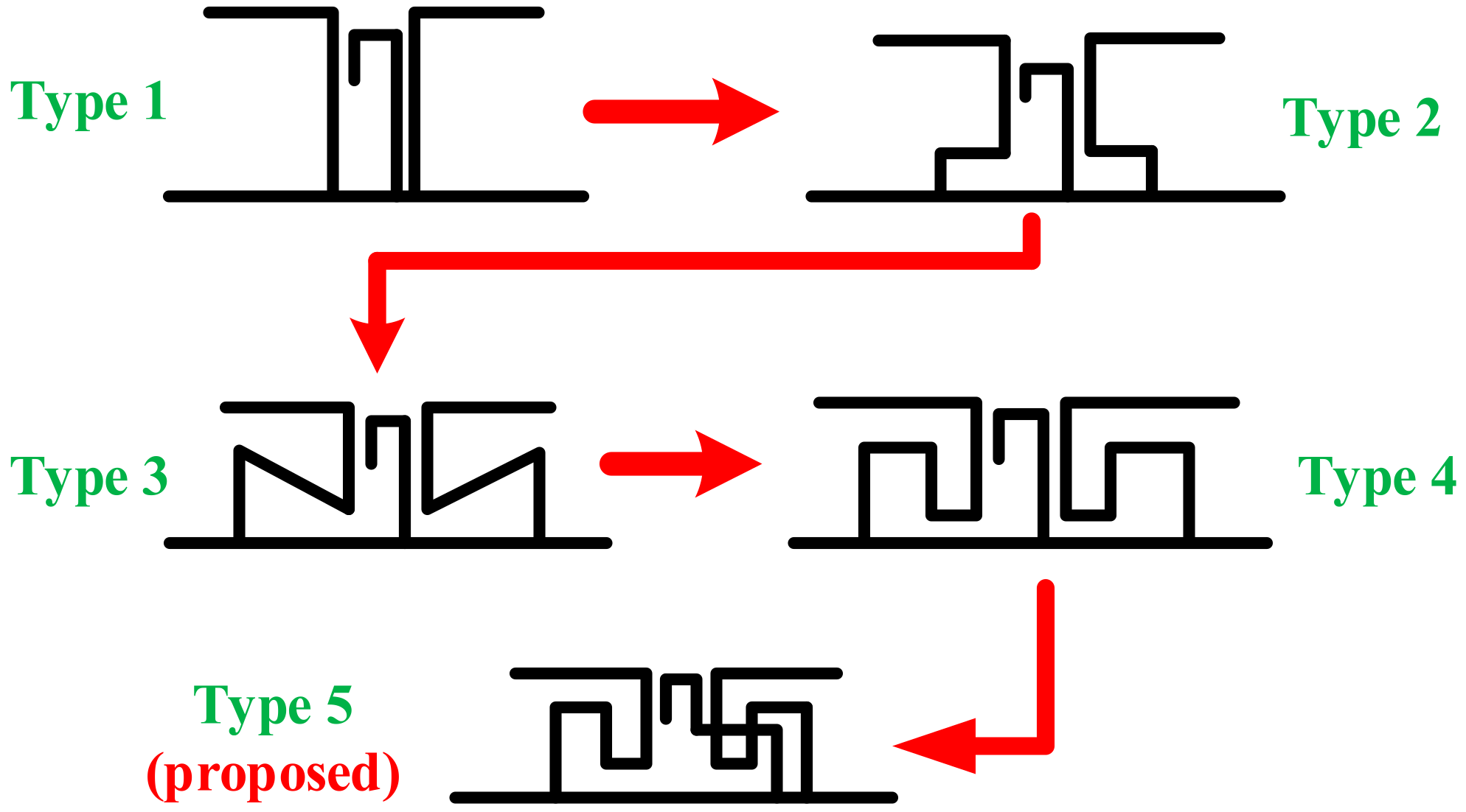
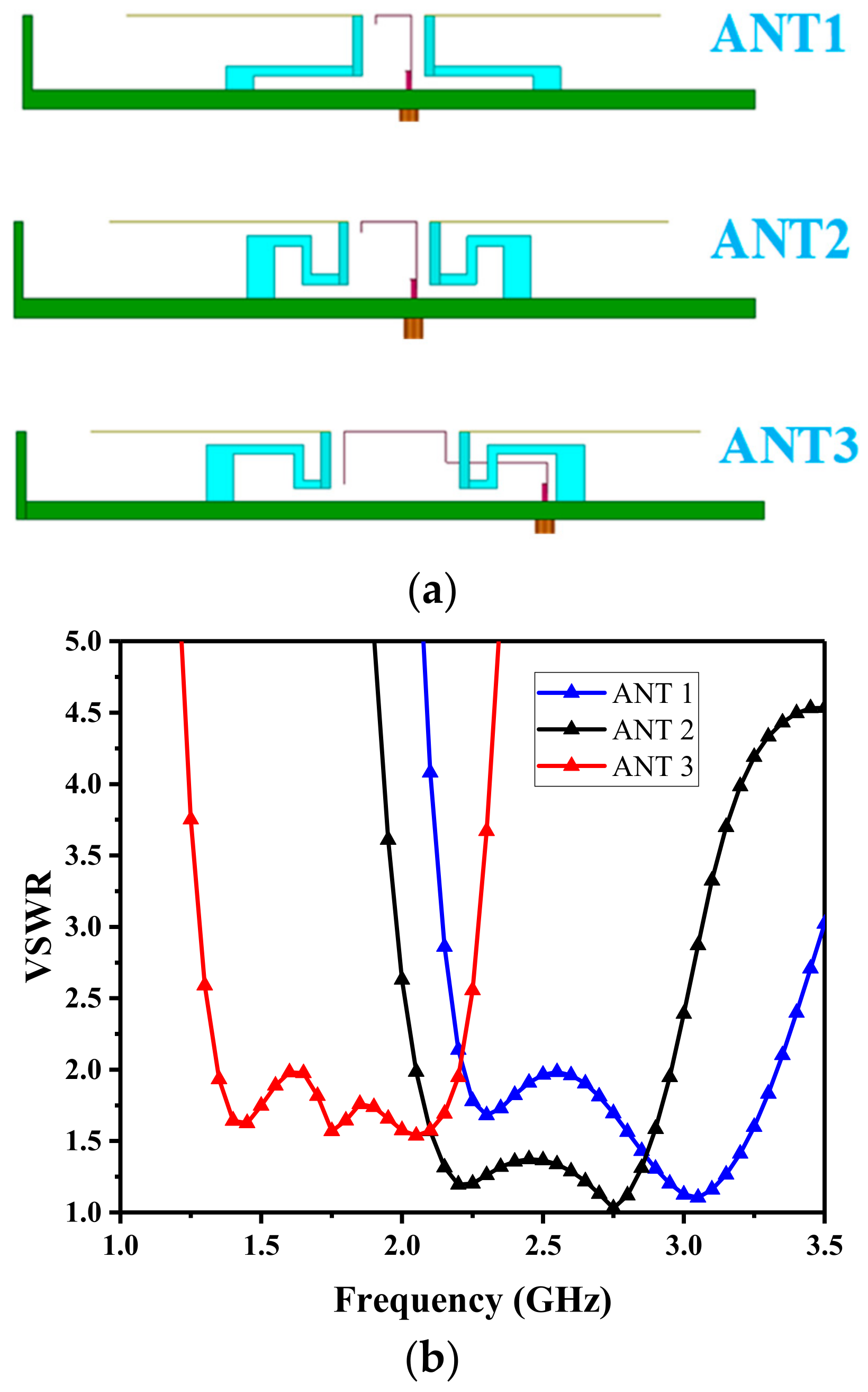
2.2. Evolution of the Proposed Antenna

To demonstrate the current low-profile technique, an evolution of the proposed ME dipole is depicted in Figure 2. Here, five evolution processes (type 1, type 2, type 3, type 4, and type 5, respectively) are depicted. Type 1 is the normal ME dipole designed by Luk [10]. By bending the vertical portion of type 1, type 2 is obtained on the right-top in Figure 2. Furtherly, type 3 and type 4 are formed by an oblique extension and a meandering process for the bending portion of type 2, as shown on the left-center and right-center in Figure 2, respectively. Finally, the proposed antenna (type 5) is obtained through bending the Γ-shaped feeding structure of type 4 to the right side.

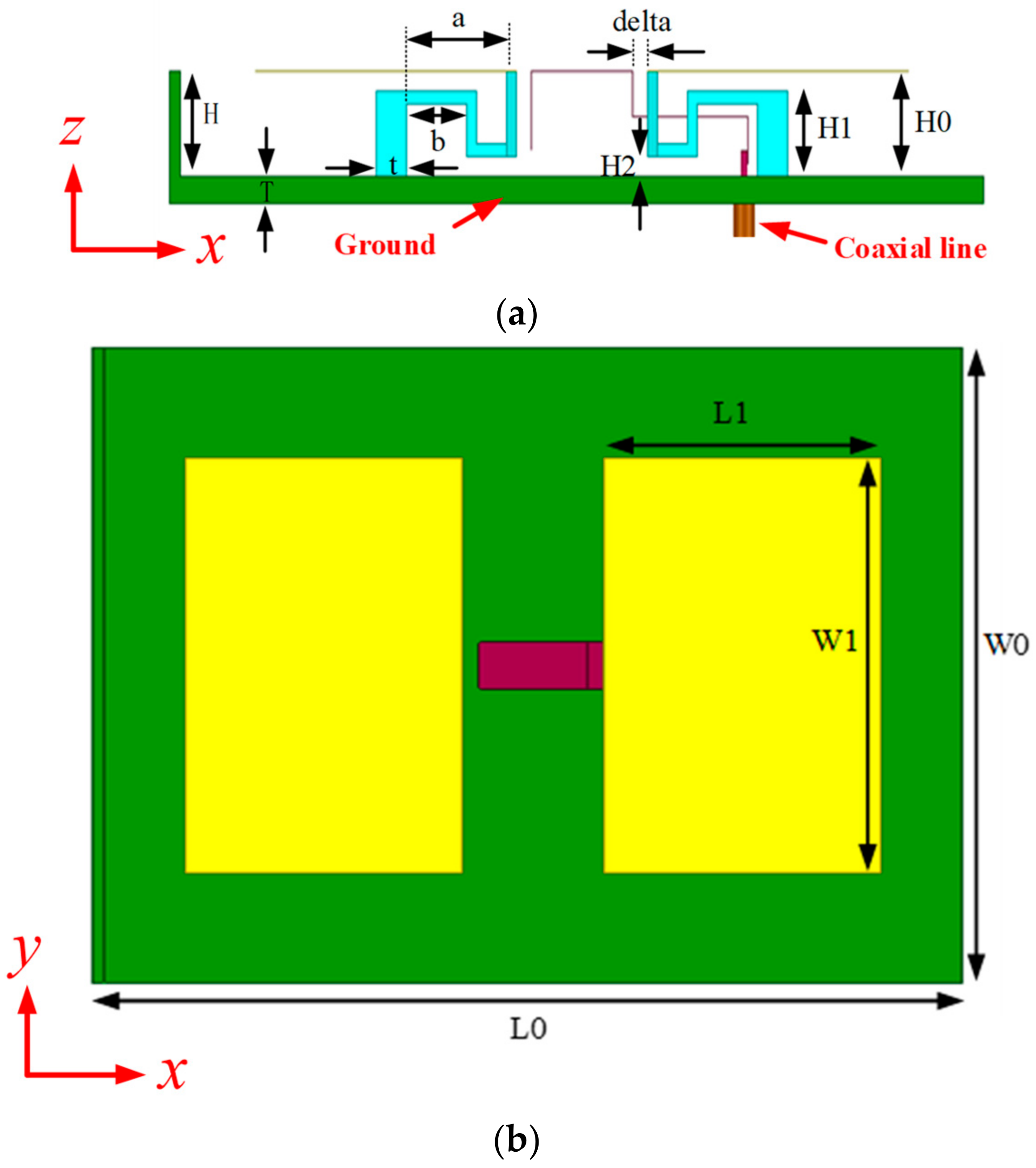
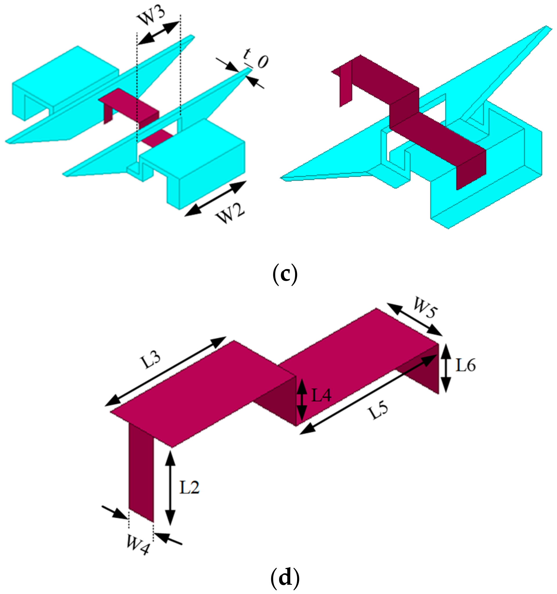
2.3. Realization of the Proposed Low-Profile ME Dipole

In this part, the structure of the proposed low-profile ME dipole is presented. The front view and top view are demonstrated in Figure 3a,b. As shown in Figure 3a, the proposed ME dipole takes the multi-bending technique as presented in Figure 2. On the one hand, the fixing structure (in blue) is bended from the center to the side four times and erected on the ground. On the other hand, the traditional Γ-shaped feeding line is bended two times to guarantee a good impedance matching to a 50 ohm coaxial line at a low-frequency band. The feeding line passes through the bended fixing structure on the right side by a rectangular slot, as depicted in Figure 3c. The detail of the feeding line is shown in Figure 3d. Finally, a vertical wall with height H is erected on the left side of the ground. The optimized sizes of the structure are listed in Table 1.
In this design, the electric dipole and the magnetic dipole is realized by the top horizontal sheet and the space between the bended fixing structure and the ground, respectively. The schematic diagram is demonstrated in Figure 4. The red arrow denotes an electric dipole and the blue arrow denotes a magnetic dipole. The combination of the electric dipole and magnetic dipole forms an ME dipole antenna.

3. Simulation, Comparison, and Analysis

3.1. VSWR for Different Evolutions

To show the low-profile property of the proposed ME dipole antenna, three types of evolution antennas (ANT 1, ANT 2, and ANT 3) are simulated and compared in this part and are shown in Figure 5. For the sake of fairness, all the antennas have the same height (H0 = 16 mm) and are well optimized. As shown in Figure 5a, these antennas from top to bottom correspond to type 2, type 4, and type 5 in Figure 2, respectively. The fixing structure for ANT 1 is only bended one time. The fixing structure for ANT 2 is bended four times. Both the fixing structure and Γ-shaped feeding line are bended for ANT 3. The optimized VSWR for the above three antennas are depicted in Figure 5b and marked by blue, black, and red, respectively. For ANT 1, the impedance bandwidth ranges from 2.25 to 3.3 GHz for VSWR < 2. For ANT 2, the impedance bandwidth ranges from 2.05 to 2.95 GHz. However, the optimized impedance bandwidth (VSWR < 2) ranges from 1.35 to 2.2 GHz for ANT 3. Furthermore, the impedance of above three antennas is also plotted in Figure 5c for comparison. Obviously, ANT 1 has a small resistance in the band of 1.35–2.2 GHz. ANT 2 has a small resistance in the band of 1.35–1.8 GHz and has a large resistance and reactance around 1.9 GHz. This leads to ANT 1 and ANT 2 being hard to match a pure 50 Ohm resistance at the input port. Meanwhile, ANT 3 increases the resistance and moderates the reactance by bending the feeding structure. It is seen that the resistance and reactance of ANT 3 is around 50 Ohm and 0 Ohm, respectively, in the band from 1.35 to 2.2 GHz. Therefore, ANT 3 can operate at a lower band and also keep the wideband characteristic when compared with ANT 1 and ANT 2 after the evolution.

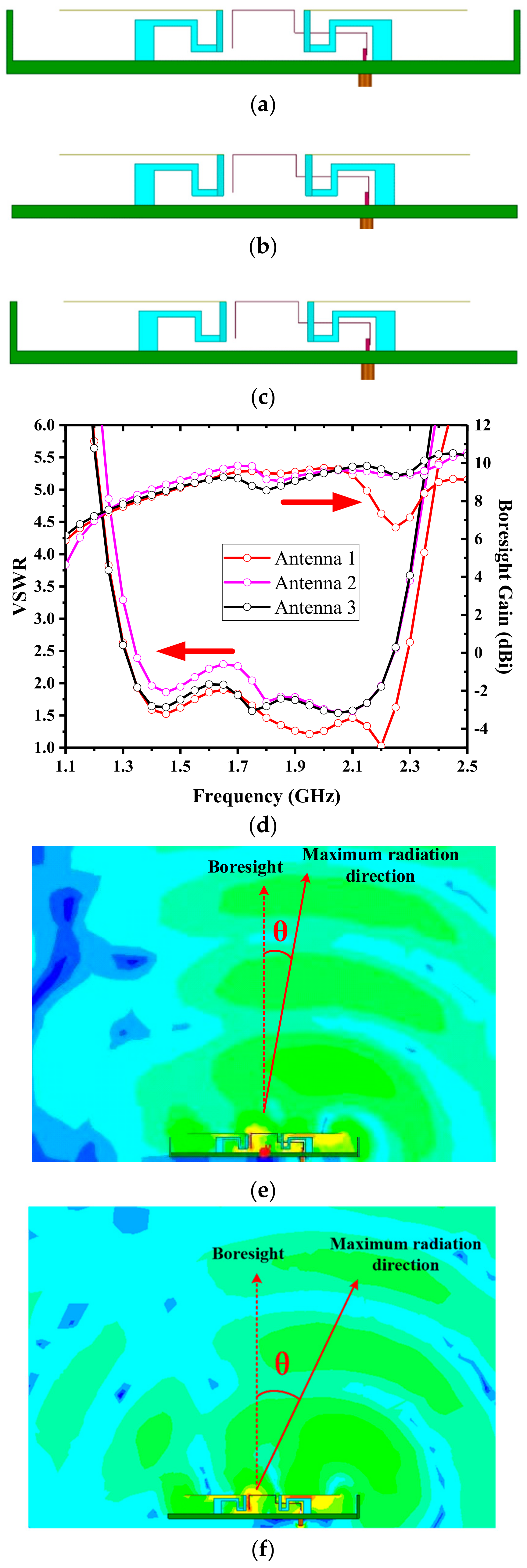
3.2. Effect of Different Grounds

The antennas with three types of ground are discussed in this section. The first type is the one with two symmetric vertical walls, as shown in Figure 6a. The second type is shown in Figure 6b. This antenna has a flat ground. The third one is our proposed antenna, which has only one vertical wall on the left side of the flat ground, as shown in Figure 6c. The above three types of antennas are named antenna 1, antenna 2, and antenna 3, respectively. The simulated VSWR and boresight gain of them are depicted in Figure 6d for comparison, simultaneously. Obviously, the impedance bandwidth (VSWR < 2) of antenna 1 and antenna 2 ranges from 1.35 to 2.25 GHz (50%) and from 1.75 to 2.2 GHz (22%), respectively. The boresight gain ranges from 6.6 to 9.7 dBi and from 9.04 to 9.6 dBi, respectively. From the red curve in Figure 6d, it is seen that a significant drop on boresight gain happens at 2.2 GHz for antenna 1. The frequency is at the upper side of the operating band. Here, we point out that this drop at 2.2 GHz for antenna 1 is due to the maximum radiation direction in E plane deviating from the boresight, as depicted in Figure 6e. The angle of deviation is θ = 10°. However, from the purple curve in Figure 6d, antenna 2 has a good boresight gain without drop but a bad VSWR at the lower band. To maintain the advantages of the impedance bandwidth of antenna 1 and the boresight gain of antenna 2 simultaneously, a method to erect only one vertical wall on the side of the ground is taken. Firstly, a single vertical wall is erected on the right side of the ground. However, the radiation field deviates from the boresight to the right side more seriously, as shown in Figure 6f. At this step, the angle of deviation is up to θ = 21°. Therefore, an idea of only erecting a single vertical wall on the left side of the ground is adopted. As the radiation field shows in Figure 6g, the maximum radiating direction is close to the boresight when the single vertical wall was erected on the left side. The angle of deviation is θ = 4° at this time. From the black curves in Figure 6d, the impedance bandwidth (VSWR < 2) of antenna 3 ranges from 1.35 to 2.2 GHz (47.9%) and the boresight gain ranges from 8.1 to 9.6 dBi. As mentioned above, antenna 3 indeed keeps the bandwidth and avoids the gain drop of antenna 1.

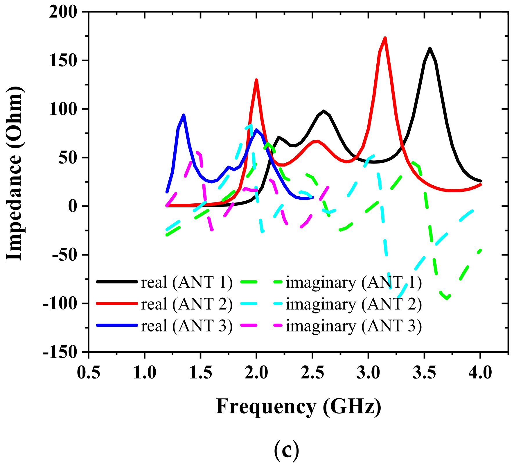
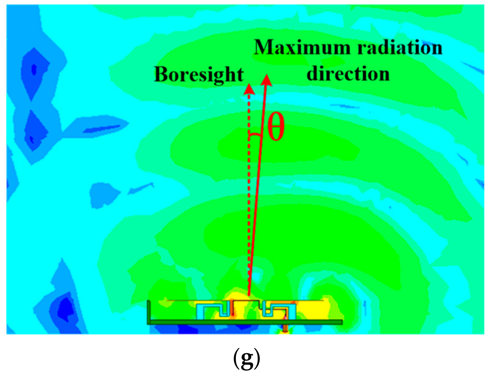
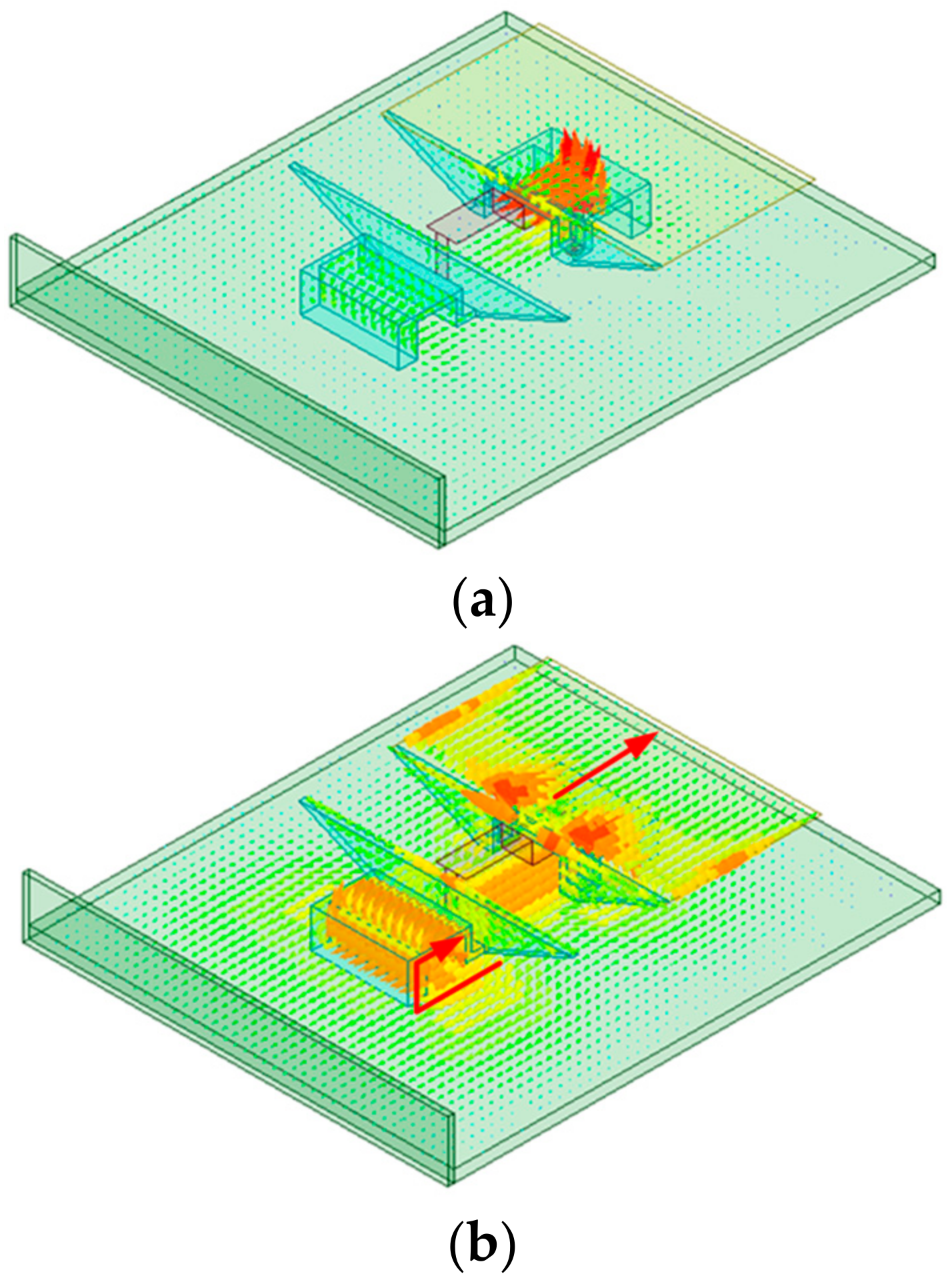
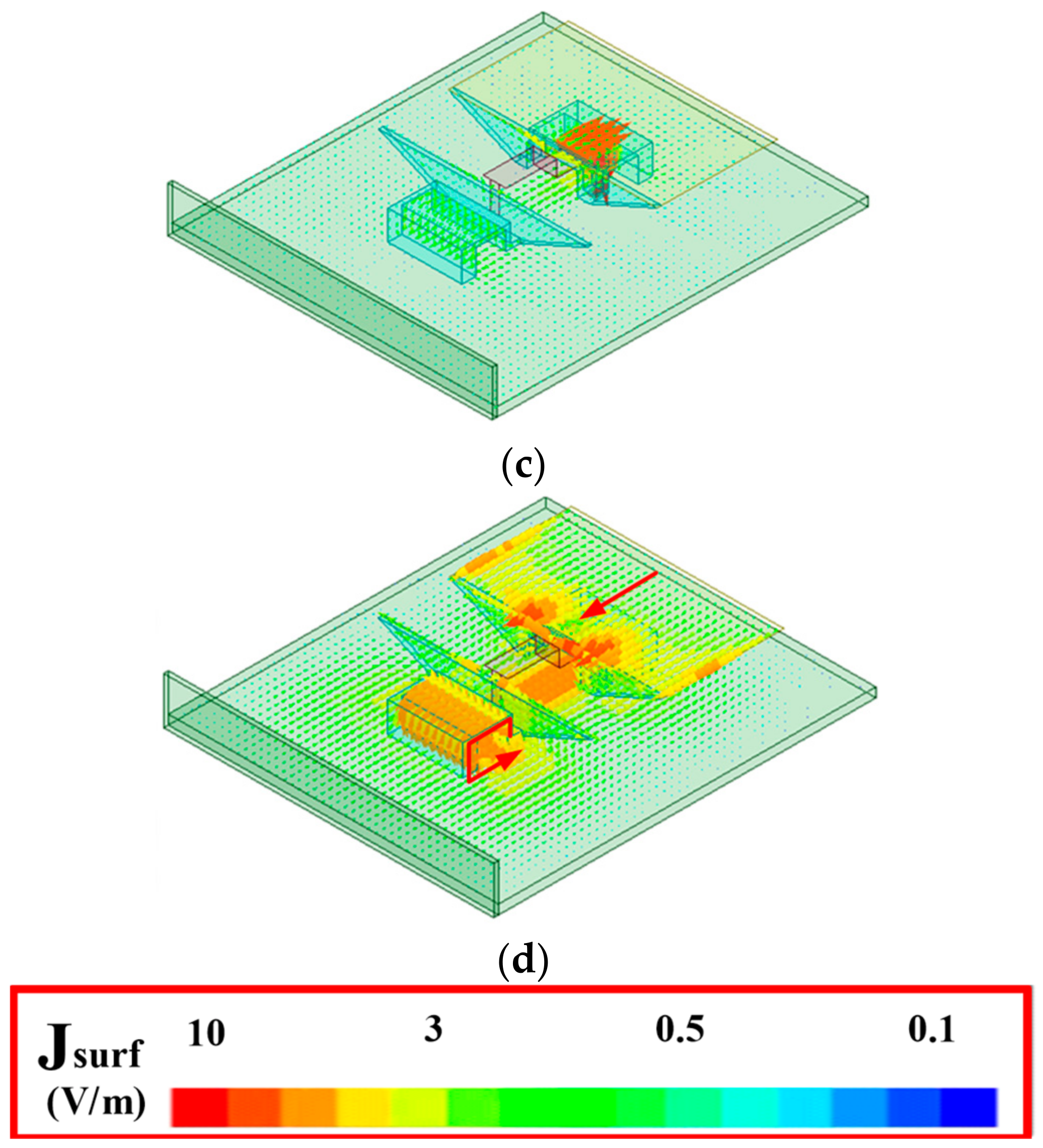
3.3. Working Mechanism

The working mechanism of the proposed antenna is analyzed by plotting the distribution of surface current. Here, it is pointed out that the proposed ME dipole antenna has its ME mode at 1.4 GHz. Therefore, the surface current in one period (1T) is given at 1.4 GHz and is shown in Figure 7. For simplicity, let t = 0 when the antenna is initially excited. As shown in Figure 7a, the surface current on the whole antenna is very weak at t = 0 and large current is just going through the feeding port to the antenna. However, the current on the top sheet, the bended surface, and the ground between these bended surfaces are strong at t = T/4, as shown in Figure 7b. The current flow is marked by a red arrow. At t = T/2, the surface current is similar to the case at t = 0 except for a reverse current flow, as shown in Figure 7c. At t = 3T/4, the current on the top sheet, the bended surface, and the ground between these bended surfaces become strong again, as shown in Figure 7d. From the principle of the ME dipole antenna shown in Figure 4, it is concluded that the electric dipole and magnetic dipole work simultaneously at t = T/4 and 3T/4 while they do not work at t = 0 and T/2.

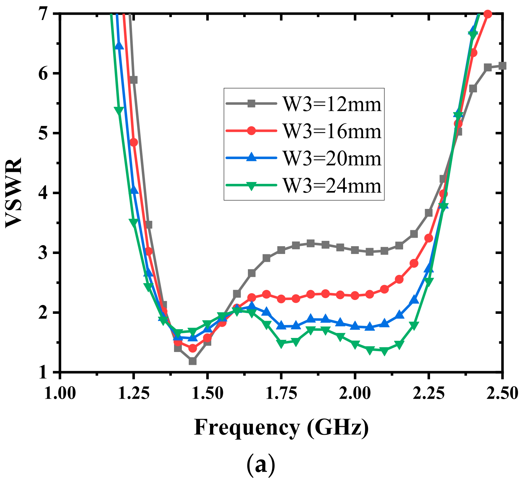
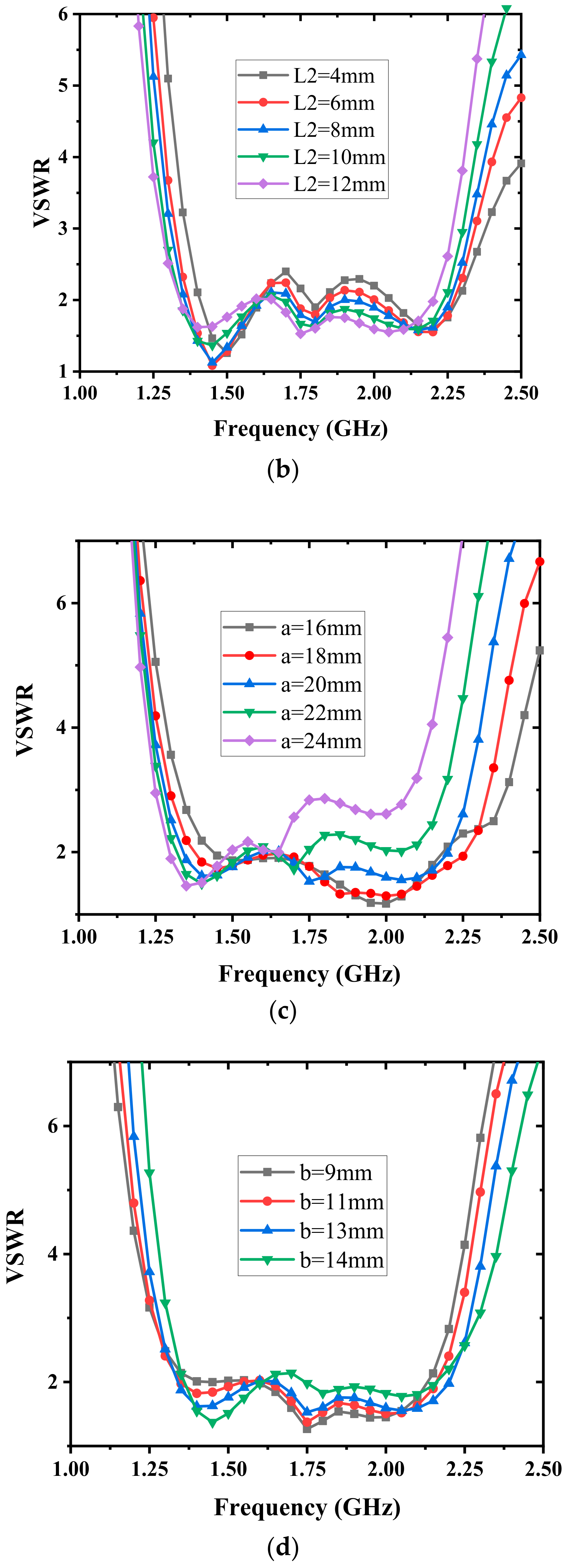
3.4. Parameter Analysis

To demonstrate the sensitivity of the structure parameters, four key parameters are discussed in this section. Firstly, W3 is chosen and analyzed. As shown in Figure 8a, with the decrease in W3 (meaning the slot on the bent structure is narrower), the VSWR on the middle and upper band becomes larger, while it becomes better around 1.45 GHz. As shown in Figure 8b, the operating band moves to a lower frequency slightly with the increase in L2. The in-band matching becomes better when L2 ranges from 4 to 12 mm. Therefore, L2 is a key parameter to make a fine tuning to the impedance matching in the operating band. As shown in Figure 8c, the VSWR on the lower band becomes better with the increase in a. However, the middle and upper bands deteriorate. As shown in Figure 8d, with the increase in b, the VSWR on the lower band also becomes better while the middle and upper bands deteriorate again. To compromise the low-profile characteristic and wideband operation, these parameters of W3 = 22 mm, L2 = 12 mm, a = 20 mm, and b = 12 mm are chosen for the proposed antenna.

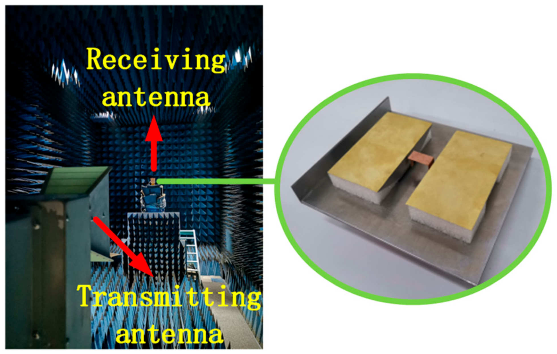
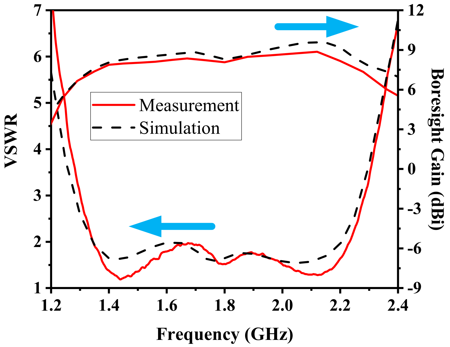
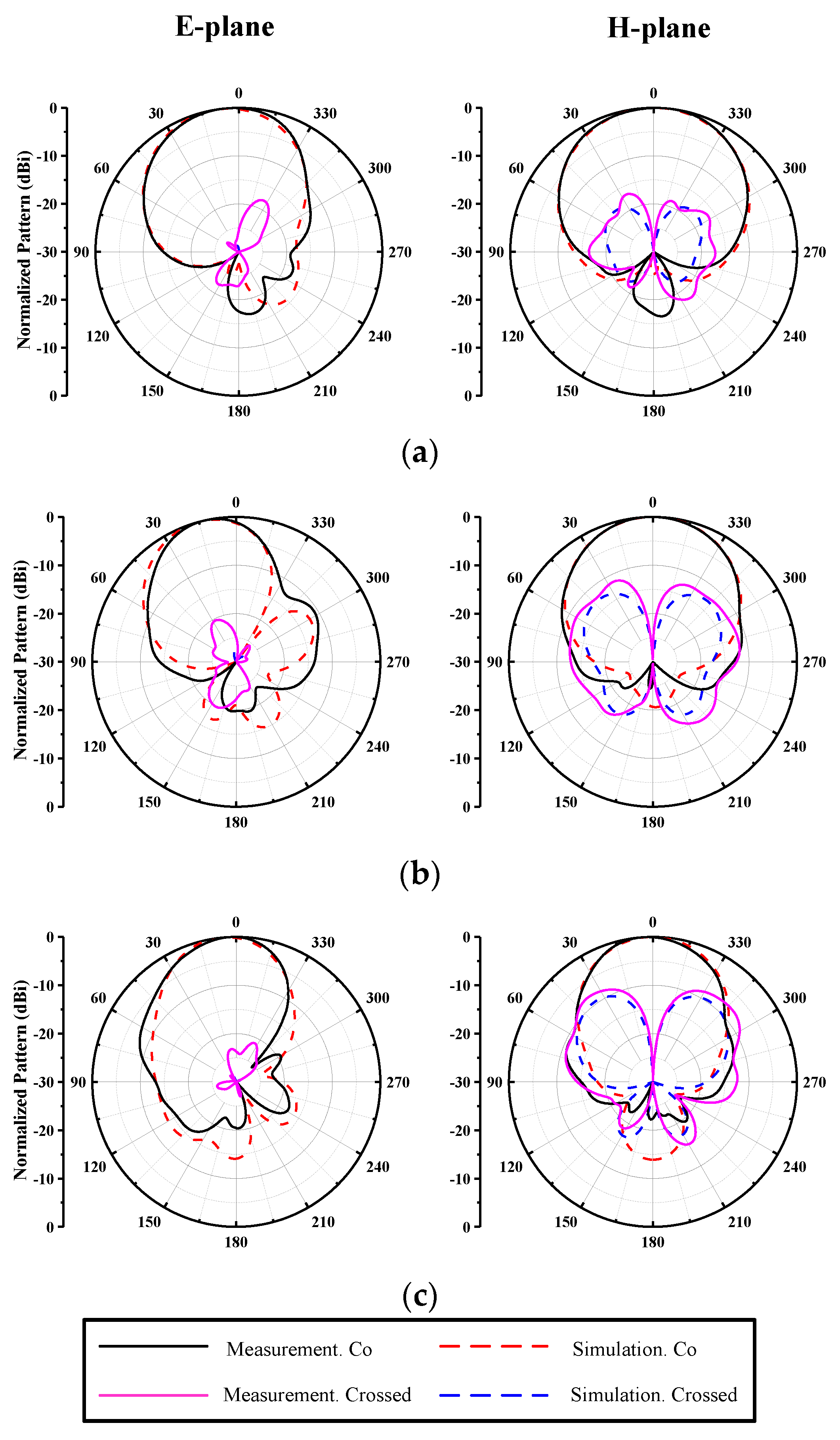
4. Fabrication and Measurement

To validate the feasibility and correctness of the proposed low-profile ME dipole antenna, a prototype has been fabricated and tested. The bended fixing structure and ground were made of aluminum. The feeding structure and the top horizontal patch were made of a thin copper sheet. To prevent the waggle of the top patches (namely, the electric dipole), two foams are adopted to support them. Finally, the prototype was tested in a microwave chamber as a receiving antenna. An ultra-wideband ridged horn (working from 500 MHz to 18 GHz) acted as a transmitting antenna, which directed to the receiving antenna, as shown in Figure 9.
The VSWR was tested by an Agilent vector network analyzer N5230A. Both simulated and measured results are plotted in Figure 10 for comparison. Obviously, the tested bandwidth for VSWR < 2 ranges from 1.34 to 2.24 GHz with a relative bandwidth of 50.3%. Considering the center operating frequency of 1.79 GHz, the profile of the antenna is only 0.095λ0. In the impedance bandwidth, the tested boresight gain ranges from 7.38 to 8.73 dBi. The gain drop in the whole band is less than 1.4 dB. Additionally, both simulated and measured normalized radiation patterns are plotted in Figure 11 at 1.4 GHz, 1.8 GHz, and 2.2 GHz for comparison. The E plane and H plane are the xoz plane and yoz plane in Figure 3, respectively. It is obvious that the radiation at the above three frequency points maintains a unidirectional property, and the cross-polarization level on boresight is less than −25 dB. Both tested and simulated patterns agree well with each other.
Finally, a performance comparison between the proposed ME dipole and other published ME dipoles is listed in Table 2. For reference [10], which is the classical ME dipole antenna, the profile is up to 0.25λ0 together with an average gain of 8 dBi. With the development of different low-profile techniques, the profile can be reduced to 0.097λ0 in reference [15]. However, the relative bandwidth is only 28.2%. In reference [17], the relative bandwidth is up to 54.8%, while the profile is only 0.173λ0. In reference [19], the antenna has a profile of 0.11λ0, but the bandwidth is only 27.6%. Among these ME dipole antennas in Table 2, the one proposed in this work is a competitive candidate in low-profile and wideband applications due to the thickness of 0.095λ0 and relative bandwidth of 50.3%.

5. Conclusions

To realize a low profile for a traditional ME dipole antenna, a multi-bending technique is proposed. Both the fixing structure and the feeding structure are bended four and two times, respectively. A profile of only 0.095λ0 in height is achieved. The effect of three different grounded antennas is analyzed and compared. At last, only one single vertical wall is erected on the left side of the ground to eliminate the gain drop at 2.2 GHz. To validate the feasibility and correctness, a prototype is fabricated and measured. By measurement, the relative bandwidth for VSWR < 2 is 50.3% (from 1.34 to 2.24 GHz). The boresight gain ranges from 7.38 to 8.73 dBi. The difference in gain is less than 1.4 dB in the whole operating band. Both the simulated and measured radiation patterns are compared at 1.4 GHz, 1.8 GHz, and 2.2 GHz to show a stable boresight radiation. The cross-polarization level on boresight is less than −25 dB. Therefore, the proposed ME dipole antenna has the advantages of lower profile and good electrical characteristics and can be used in the future low-profile applications.

Author Contributions

Conceptualization, X.C.; methodology, Z.L.; software, Z.L., Y.T. and L.L.; validation, L.D. and Z.Z.; formal analysis, Z.L.; investigation, Z.L.; resources, Z.L.; data curation, Z.L. and X.C.; writing—original draft preparation, Z.L.; writing—review and editing, X.C.; visualization, L.D. and Z.Z.; supervision, X.C.; project administration, X.C.; funding acquisition, X.C. All authors have read and agreed to the published version of the manuscript.

Funding

This work is supported by the National Natural Science Foundation of China under Grant number U19A2054.

Data Availability Statement

Data is contained within the article.

Conflicts of Interest

The authors declare no conflict of interest.

References

  1. Schantz, H. The Art and Science of Ultrawideband Antennas, 2nd ed.; Artech House Antennas and Propagation Library: Boston, MA, USA, 2015. [Google Scholar]
  2. Xiao, S.; Wang, B.-Z.; Shao, W.; Zhang, Y. Bandwidth-enhancing ultralow-profile compact patch antenna. IEEE Trans. Antennas Propag. 2005, 53, 3443–3447. [Google Scholar] [CrossRef]
  3. Liu, W.; Chen, Z.N.; Qing, X. Metamaterial-based low-profile broadband mushroom antenna. IEEE Trans. Antennas Propag. 2013, 62, 1165–1172. [Google Scholar] [CrossRef]
  4. Liu, W.; Chen, Z.N.; Qing, X. Metamaterial-based low-profile broadband aperture-coupled grid-slotted patch antenna. IEEE Trans. Antennas Propag. 2015, 63, 3325–3329. [Google Scholar] [CrossRef]
  5. Pan, Y.M.; Hu, P.F.; Zhang, X.Y.; Zheng, S.Y. A low-profile high-gain and wideband filtering antenna with metasurface. IEEE Trans. Antennas Propag. 2016, 64, 2010–2016. [Google Scholar] [CrossRef]
  6. Wang, X.-Y.; Tang, S.-C.; Shi, X.-F.; Chen, J.-X. A low-profile filtering antenna using slotted dense dielectric patch. IEEE Antennas Wirel. Propag. Lett. 2019, 18, 502–506. [Google Scholar] [CrossRef]
  7. Cheng, B.; Du, Z.; Huang, D. A broadband low-profile multimode microstrip antenna. IEEE Antennas Wirel. Propag. Lett. 2019, 18, 1332–1336. [Google Scholar] [CrossRef]
  8. An, W.; Li, S.; Sun, W.; Li, Y. Low-profile wideband microstrip antenna based on multiple modes with partial apertures. IEEE Antennas Wirel. Propag. Lett. 2019, 18, 1372–1376. [Google Scholar] [CrossRef]
  9. Chlavin, A. A new antenna feed having equal e- and h-plane patterns. Trans. IRE Prof. Group Antennas Propag. 1954, 2, 113–119. [Google Scholar] [CrossRef]
  10. Luk, K.M.; Wong, H. A new wideband unidirectional antenna element. Int. J. Microw. Opt. Technol. 2006, 1, 35–44. [Google Scholar]
  11. Chen, S.; Luk, K.M. A dual-mode wideband MIMO cube antenna with magneto-electric dipoles. IEEE Trans. Antennas Propag. 2014, 62, 5951–5959. [Google Scholar] [CrossRef]
  12. Cui, X.; Yang, F.; Gao, M.; Zhou, L.; Liang, Z.; Yan, F. A Wideband magnetoelectric dipole antenna with microstrip line aperture-coupled excitation. IEEE Trans. Antennas Propag. 2017, 65, 7350–7354. [Google Scholar] [CrossRef]
  13. Lai, H.W.; Wong, H. Substrate integrated magneto-electric dipole antenna for 5G Wi-Fi. IEEE Trans. Antennas Propag. 2014, 63, 870–874. [Google Scholar] [CrossRef]
  14. Luk, K.M.; Wu, B. The magnetoelectric dipole—A wideband antenna for base stations in mobile communications. Proc. IEEE 2012, 100, 2297–2307. [Google Scholar] [CrossRef]
  15. Ding, C.; Luk, K.M. Low-profile magneto-electric dipole antenna. IEEE Antennas Wirel. Propag. Lett. 2016, 15, 1642–1644. [Google Scholar] [CrossRef]
  16. Ge, L.; Gao, S.; Zhang, D.; Li, M. Magnetoelectric dipole antenna with low profile. IEEE Antennas Wirel. Propag. Lett. 2018, 17, 1760–1763. [Google Scholar] [CrossRef]
  17. Ge, L.; Luk, K.M. A low-profile magneto-electric dipole antenna. IEEE Trans. Antennas Propag. 2012, 60, 1684–1689. [Google Scholar] [CrossRef]
  18. Ge, L.; Luk, K.M. A magneto-electric dipole antenna with low-profile and simple structure. IEEE Antennas Wirel. Propag. Lett. 2013, 12, 140–142. [Google Scholar] [CrossRef]
  19. Yang, S.J.; Pan, Y.M.; Zhang, Y.; Gao, Y.; Zhang, X.Y. Low-profile dual-polarized filtering magneto-electric dipole antenna for 5G applications. IEEE Trans. Antennas Propag. 2019, 67, 6235–6243. [Google Scholar] [CrossRef]
Figure 1. A depiction of the current low-profile techniques for an ME dipole antenna. (a) antenna 1; (b) antenna 2; (c) antenna 3; (d) antenna 4.
Electronics 11 01156 g001
Figure 2. The evolution of the proposed low-profile ME dipole.
Electronics 11 01156 g002
Figure 3. The structure of the proposed low-profile ME dipole. (a) Front view, (b) top view, (c) bended fixing structure, (d) feeding line.
Electronics 11 01156 g003aElectronics 11 01156 g003b
Figure 4. The schematic diagram of electric dipole and magnetic dipole.
Electronics 11 01156 g004
Figure 5. (a) The structure of ANT 1, ANT 2, and ANT3; (b) VSWR of ANT 1, ANT 2, and ANT3; (c) impedance of ANT 1, ANT 2, and ANT 3.
Electronics 11 01156 g005aElectronics 11 01156 g005b
Figure 6. The structure of the antenna with (a) two symmetric vertical walls; (b) only flat ground plane; (c) one vertical wall; (d) the VSWR for different ground; (e) the radiating E field at 2.2 GHz for antenna 1; (f) the radiating E field at 2.2 GHz for the antenna with the single vertical wall on the left side; (g) the radiating E field at 2.2 GHz for antenna 3.
Electronics 11 01156 g006aElectronics 11 01156 g006b
Figure 7. The distribution of electric current in one period. (a) at t = 0, (b) at t = T/4, (c) at t = T/2, (d) at t = 3T/4.
Electronics 11 01156 g007aElectronics 11 01156 g007b
Figure 8. The parameter analysis for (a) W3, (b) L2, (c) a, and (d) b.
Electronics 11 01156 g008aElectronics 11 01156 g008b
Figure 9. The measurement of proposed antenna.
Electronics 11 01156 g009
Figure 10. The comparison of simulated VSWR and boresight gain.
Electronics 11 01156 g010
Figure 11. The simulated and measured radiation patterns at (a) 1.4 GHz, (b) 1.8 GHz, (c) 2.2 GHz.
Electronics 11 01156 g011
Table 1. Parameter size of the low-profile ME dipole antenna (unit: mm).
L0L1L2L3L4L5L6W0W1W2
162
(0.97λ0)
52
(0.31λ0)
12
(0.07λ0)
20
(0.12λ0)
7
(0.04λ0)
23
(0.14λ0)
7
(0.04λ0)
140
(0.84λ0)
91
(0.54λ0)
32
(0.19λ0)
W3W4W5Ttt_0HH0H1H2
22
(0.13λ0)
4
(0.02λ0)
10
(0.06λ0)
4
(0.02λ0)
6
(0.04λ0)
2
(0.01λ0)
16
(0.095λ0)
16
(0.095λ0)
13
(0.08λ0)
3
(0.018λ0)
abDelta
20
(0.12λ0)
12
(0.07λ0)
3
(0.018λ0)
Table 2. The performance comparison between the proposed antenna and other ME dipoles.
ReferenceProfileCenter
Frequency
BandwidthAverage GainGain DropLateral Dimension
[10]0.25λ02.37 GHz43.8%8 dBi0.7 dBi0.95λ0 × 0.95λ0
[13]0.11λ05.495 GHz18.74%7 dBi0.4 dBi0.66λ0 × 0.66λ0
[15]0.097λ01.945 GHz28.2%9.2 dBi2.2 dBi0.99λ0 × 0.99λ0
[16]0.116λ02.315 GHz43.6%9 dBi7.4 dBi0.88λ0 × 0.88λ0
[17]0.173λ02.59 GHz54.8%8.6 dBi2 dBi0.97λ0 × 0.97λ0
[18]0.169λ01.68 GHz45.6%8.1 dBi1.6 dBi1.04λ0 × 1.04λ0
[19]0.11λ03.75 GHz27.6%8.2 dBi2.2 dBi0.75λ0 × 0.75λ0
Proposed0.095λ01.96 GHz50.3%8.06 dBi1.4 dBi0.96λ0 × 0.83λ0
Publisher’s Note: MDPI stays neutral with regard to jurisdictional claims in published maps and institutional affiliations.

