Article

Efficient FPGA Implementation of an ANN-Based Demapper Using Cross-Layer Analysis

1
Microelectronic Systems Design Research Group, Department of Electrical and Computer Engineering, Technical University of Kaiserslautern, 67663 Kaiserslautern, Germany
2
Institute of Telecommunications, Department of Electrical Engineering and Information Technology, University of Stuttgart, 70174 Stuttgart, Germany
*
Author to whom correspondence should be addressed.
Electronics 2022, 11(7), 1138; https://doi.org/10.3390/electronics11071138
Submission received: 9 March 2022 / Revised: 28 March 2022 / Accepted: 1 April 2022 / Published: 3 April 2022

Abstract

:
In the field of communication, autoencoder (AE) refers to a system that replaces parts of the traditional transmitter and receiver with artificial neural networks (ANNs). To meet the system performance requirements, it is necessary for the AE to adapt to the changing wireless-channel conditions at runtime. Thus, online fine-tuning in the form of ANN-retraining is of great importance. Many algorithms on the ANN layer are developed to improve the AE’s performance at the communication layer. Yet, the link of the system performance and the ANN topology to the hardware layer is not fully explored. In this paper, we analyze the relations between the design layers and present a hardware implementation of an AE-based demapper that enables fine-tuning to adapt to varying channel conditions. As a platform, we selected field-programmable gate arrays (FPGAs) which provide high flexibility and allow to satisfy the low-power and low-latency requirements of embedded communication systems. Furthermore, our cross-layer approach leverages the flexibility of FPGAs to dynamically adapt the degree of parallelism (DOP) to satisfy the system-level requirements and to ensure environmental adaptation. Our solution achieves 2000× higher throughput than a high-performance graphics processor unit (GPU), draws 5× less power than an embedded central processing unit (CPU) and is 5800× more energy efficient compared to an embedded GPU for small batch size. To the best of our knowledge, such a cross-layer design approach combined with FPGA implementation is unprecedented.

1. Introduction

1.1. From Communication System Layer to Artificial Neural Network Layer

Communication systems have been rapidly evolving over the last two decades. While the provided data rates are in the order of 10 kbps in the second-generation Global System for Mobile Communication (2G/GSM), the new standard 5G is supporting more than 10 Gbps, and the expected rate is increasing towards 1 Tbps in beyond 5G and 6G-era.
The traditional principle for designing such a digital baseband wireless system can be divided into two steps:
(1)
Partitioning of the processing blocks at the transmitter and receiver into different subcomponents, e.g., source coding, channel coding, and modulation;
(2)
Optimizing each subcomponent individually for a channel model while considering the application requirements.
Although it is known how to optimally configure each component separately, this configuration does not assure the ideal communication performance of the joint system [1]. In addition, the channel model is not able to perfectly emulate all properties of a real-world channel due to model imperfections and hardware impairments. Therefore, a degradation of the performance in real channel conditions is witnessed. To mitigate this effect, ANN-based methods have gained a lot of attention in the field of communication in recent years [2,3,4,5]. The challenge is to have highly functional communication systems competing with the system-level performance of the conventional ones and overcoming the need for prior mathematical modeling of the channel.
The AE approach, where parts of the classical transmitter and receiver are replaced by artificial neural networks (ANNs), has delivered promising results [6,7,8,9,10]. Since the AE is designed as an end-to-end system, all components can be jointly trained to optimize the global system instead of adjusting each block individually; thus, the sub-optimal performance of the classical approach introduced by (1) can be resolved. Furthermore, ANNs provide the functionality to compensate for imperfections of the channel model and hardware impairments by retraining the network during runtime to adapt for the actual channel conditions, which tackles the drawbacks of (2) in the conventional system design.

1.2. From Neural Networks Layer to Hardware Layer

ANNs were introduced as an approach to reduce the design complexity by looking at the overall communication system (or major components of it) as one big block, instead of optimizing internal blocks individually [11,12,13]. While different proposed solutions can meet and overcome the performance of traditional communication algorithms [14,15], whenever dealing with ANN-based methods, the high memory demand and computational requirements raise the implementation complexity. This leads to high power and energy consumption, which is critical, especially for embedded communication systems. This is one reason why ANN solutions had no fundamental impact on the practical implementation of baseband processing systems so far.
In this context, three major challenges are of high importance:
  • Low-latency, which is essential for delay-sensitive applications;
  • Low-power, which is mandatory to meet the constraints of embedded devices;
  • Adaptability, which is of high relevance due to the varying channel conditions.
General-purpose processors such as graphics processor units (GPUs) or central processing units (CPUs) are not able to satisfy all those constraints at once. In contrast, FPGAs provide a platform that can meet the requirements of our intended application. They offer a flexible memory hierarchy, arbitrary precision datatypes, custom datapaths, as well as huge bit-level parallelism, which allows to implement ANNs in an extremely energy-efficient manner [16,17,18].
The majority of FPGA-based ANN architectures target the inference only, by training the network in software and exporting the trained parameters to optimize inference engines. This approach is not sufficient for the AE application proposed in this work because retraining to adapt to channel fluctuations is of high importance. Therefore, we tackle the challenges of designing a low-latency, low-power architecture for inference and training of the AE on the edge device. To efficiently exploit the capabilities of FPGAs, we integrate our architecture into a framework that automatically selects the DOP for the inference and training module to satisfy the application requirements and optimize for power or latency.

1.3. Our Work as Cross-Layer Approach

State-of-the-art communication algorithms are already optimized for efficient implementation on edge devices by trading-off communication performance against hardware complexity. In contrast, most research in ANN-based communication only focuses on the algorithmic level without considering the feasibility of the implementation. However, an efficient hardware implementation is mandatory for a fair comparison to conventional systems. This challenge of designing an efficient architecture for ANN-based communication systems can be abstracted into three design layers: Communication Layer, ANN Layer and Hardware Layer. Those layers are not independent but highly influence each other; therefore, a joint analysis is of high importance for efficient cross-layer design. In our work, we target this challenge by taking into consideration the relations between the layers during our design process. We evaluate how the convergence latency of the ANN layer is related to the signal-to-noise ratio (SNR) of the communication layer and additionally provide a link to the hardware layer in terms of DOP. We exploit this interaction in a framework that calculates the optimal degree of parallelisms (DOPs) for given application requirements. This allows us to tackle the challenge of optimizing communication performance, while taking into account the limitations and constraints posed by the hardware device, in our case the limited FPGA resources.
In summary, the novel contributions of this paper are:
  • A cross-layer approach that relates the application requirements (SNR, bit error rate (BER)) to the ANN architecture (time of convergence for training the ANN) and to the hardware implementation capabilities (DOP, utilization of the FPGA resources);
  • The evaluation of the hardware performance of a trainable demapper in the context of AE-based communication systems that enables online fine-tuning to the latest noise conditions in wireless channels. To the best of our knowledge, such an FPGA implementation is unprecedented;
  • A parameterizable framework that enables the adjustment of the DOPs to satisfy the application requirements, to ensure environmental adaptation and optimize latency or power;
  • A benchmark of the highly efficient FPGA design by comparing the performance to a PyTorch implementation on a high-performance GPU, an embedded GPU, and an embedded CPU.

2. Related Work

2.1. AE for Communication

The approach of training an end-to-end communication system was first proposed by O’Shea et al. in 2017 [6]. Transmitter and receiver are designed as feedforward ANN with multiple dense layers and a normalization layer to ensure power constraints, whereas the channel is represented as an additive noise layer. The complete system is referred to as AE which is a long-known concept in the field of deep learning (DL) ([19], Chapter 14). In [6], the system is trained to reduce the block error rate (BLER) and compared to a baseline that uses a Hamming (7,4) code and binary phase shift keying (BPSK) modulation. As a result, the end-to-end system achieves a gain of up to 1 dB due to the joint coding and modulation scheme.
The previously mentioned AEs are optimized based on the symbol-wise categorical cross-entropy loss and therefore minimizing the BLER of the receiver. As described in [10], practical systems can benefit from maximizing the bitwise mutual information that is proven to be an achievable rate for bit-metric decoding (BMD) and, thus, bit interleaved coded modulation (BICM) can be applied. Additionally, when trained to minimize the BLER, the learned constellation points must be labeled by bit vectors, which can be a highly sophisticated task. To overcome this limitation, the AE can be trained to directly optimize the bit-metrics, referred to as bitwise AE in the following. This approach was first described by Alberge et al. in 2019 [20]. They applied the AE concept to a channel modeling additive radar inference in which standard constellations are not optimal and showed that the AE is able to yield solutions that outperform the standard configurations.
The idea of a bitwise AE is further evaluated and extended in [10]. On the one hand, the approach is applied to the BICM scenario, and on the other hand, the universality of the method is practically demonstrated and implemented on software-defined radios. Additionally, it is investigated how low-density parity-check (LDPC) codes can be optimized after the system is trained to achieve further gains.
This concept of an AE-based communication system was first demonstrated via over-the-air measurements in [21]. After the initial model-based training, the encoder and decoder parts were separated and deployed as transmitter and receiver, respectively, where the transmission and recording of the AE-generated signals were realized using software-defined radios (SDRs). As the channel model does not cover all impairments that are later present via over-the-air transmission, a second training step to adapt the decoder part at the receiver to the actual channel and hardware impairments is proposed. Therefore, a large dataset of known AE messages was transmitted and recorded at receiver side over the real channel and then used for supervised re-training of the decoder ANN. This approach of re-training, or fine-tuning, showed improved performance. Therefore, in this work, using the bitwise AE structure presented in [10], we will focus on the trainable demapper that enables online fine-tuning to latest noise conditions in wireless channels.

2.2. FPGA-Based Neural Network Training Accelerators

Various FPGA implementations of ANNs only target the inference of the network as there is no need for retraining on FPGA, since environmental conditions do not change for most applications. Additionally, GPUs provide sufficient performance for offline training in many cases. However, there are multiple works that concentrate on the design of ANN training modules for FPGAs, described in the following.
In 2018, Geng et al. presented FPDeep, which is a scalable framework that helps map the training logic of an ANN to a multi-FPGA cluster with up to 60 devices [22]. They applied a strategy to balance the workload between different FPGAs and execute the training in a fine-grained inter- and intra-layer pipelined manner, minimizing the time that features need to remain available while waiting for back-propagation. Another framework called DarkFPGA was proposed by Luo et al. in 2020 [23]. It accelerates ANN training on a single FPGA platform by exploring concurrency on batch-level and uses tiling techniques to effectively exploit parallelism. They outperform FPDeep in terms of performance per FPGA and are 5 times more energy-efficient compared to the same network running on an Nvidia GTX 1080 Ti. A different approach is presented by Nakahara et al. in 2019 [24]. Their accelerator utilizes the sparseness of CNNs to reduce the number of parameters by approximately 85%. Thus, they are able to store all parameters on-chip to accelerate the training computation and reduce power consumption by eliminating energy-consuming DRAM accesses. They applied their method to AlexNet [25], VGG16 [26] and MobileNet [27] resulting in four times faster runtime than the Nividia RTX 2080 Ti. Another compression technique, specifically datatype precision reduction, was used by DiCecco et al. [28]. The FPGA-based CNN training engine includes custom-precision floating-point cores for multiplication and addition to reduce the resource utilization. Liu et al. proposed a scalable accelerator framework in 2017 and applied it to multiple CNNs [29]. They presented a uniform computation engine which can exploit parallelism by unrolling loops on two levels. They achieved a speedup of 10.7 compared to CPU and higher energy efficiency than the Nvidia GTX 1080 Ti GPU. In 2019, Venkataramanaiah et al. presented an FPGA training accelerator which is based on an automatic RTL compiler and makes use of a new cyclic weight storage scheme [30]. Their FPGA implementation achieves less throughput but higher energy efficiency than the Nvidia Titan XP GPU.
A work targeting the inference and training on low-power and energy-constrained edge devices was proposed by Hong et al. in 2021 [31]. Their accelerator makes use of pruning along with quantization and is implemented on FPGA and silicon for the MNIST dataset. They compared their implementation to [29,30], achieving a much lower power consumption, while the normalized energy consumption is in the same order of magnitude. In this work, we propose an on-chip architecture that is based on a low-complexity ANN with a small memory footprint to reduce power consumption while still outperforming general-purpose processors in terms of latency and energy efficiency.

3. System Model

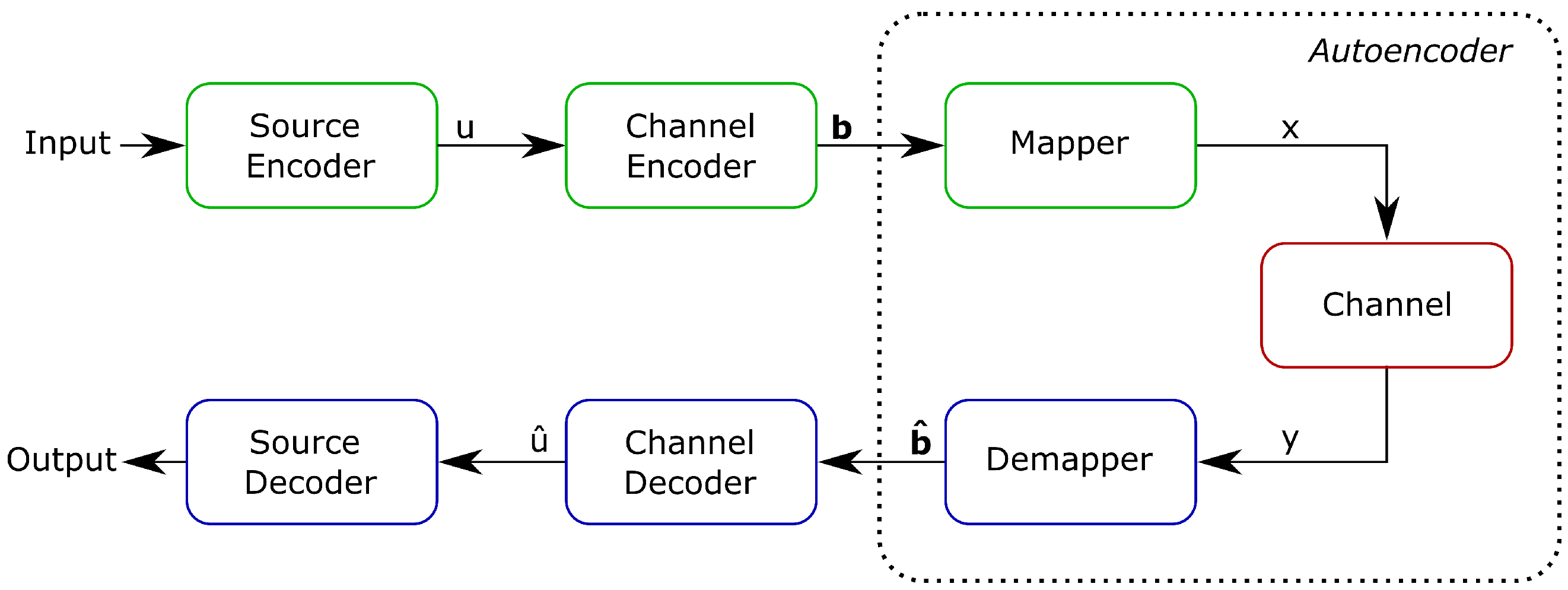
3.1. Communication System
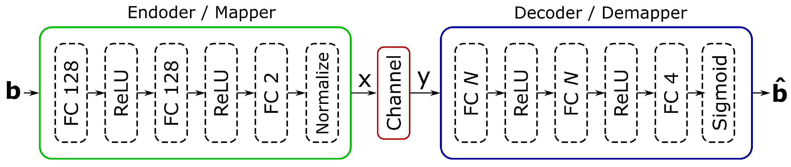
A digital communication system consists of a transmitter and a receiver with the goal of reliably transmitting information over a noisy channel, as seen in Figure 1.
Transmitter and receiver comprise several building blocks to compress the source information (source encoder, source decoder), overcome the distortion and noise introduced by the channel by increasing redundancy (channel encoder, channel decoder), and to convert the signal to a more robust representation (mapper, demapper). In this work, we focus on mapper and demapper blocks. At the transmitter side, multiple information bits b are commonly mapped to a complex symbol x that is transmitted over the channel. The received symbol y is then demapped to bits b ^ at receiver side. In the case of four bits per symbol, the 16-quadrature amplitude modulation (QAM) constellation is widely used in conventional systems, where the constellation points are arranged in a square grid with equal vertical and horizontal spacing.
For evaluation of a communication system, abstract channel models are used to mimic the characteristics of a real channel. The most basic model is the additive white Gaussian noise (AWGN) channel, where uncorrelated Gaussian noise n C N ( 0 , σ 2 ) with noise power N 0 = σ 2 is added to the input message x to obtain y = x + n . Here, the SNR determines the ratio between the average signal power E s = E x 2 and the noise power. In our case, where we focus on m = 4 bit per complex-valued symbol, the SNR corresponds to the energy per bit E b = E s / m per noise power spectral-density and is defined as
S N R = E b N 0 .
To measure the final reliability of a communication chain (after the decoder), hard-decided BER, as well as BLER, can be used, giving either the amount of incorrectly predicted bits or incorrectly predicted bit block sequences. However, as today’s communication chains usually rely on practical BMD receivers, which process soft bit estimates, i.e., logarithmic likelihood ratio (LLRs), the optimal BMD-based metric for the output of the demapper is bitwise mutual information (MI) [32] which refers to the average amount of information one gains in comparison with the originally transmitted bits when observing the received symbols. The bitwise MI is given as
BMI H ( B ) j = 1 m H ( B j | Y )
where B denotes the binary random variable providing the input bits b of length m, H denotes the entropy, and Y denotes the random variable associated with the received symbol y. We estimate the bitwise MI in the following via Monte Carlo simulation of large numbers of bits.

3.2. Autoencoder

As it is described in Section 1, an AE refers to a trainable end-to-end communication system, consisting of ANNs at transmitter and receiver side and a differentiable channel model in between. This work focuses on implementing the mapper and demapper blocks of the communication chain as ANN, as shown in Figure 1.
The mapper defines a building block that takes an input vector consisting of m bits (or as one-hot-coded input vector of length M = 2 m ) and maps it to a complex-valued constellation symbol, which is then transmitted over a channel. The goal of the mapper is to find a symbol constellation that conveys the maximal amount of information at the given system settings. Subsequently, the demapper receives the corresponding complex symbol that is impaired by the noise of the channel. Its goal is to provide the most reliable estimate of the originally transmitted bits in form of m output probabilities.
Similar to [10], our mapper and demapper ANNs comprise three fully connected layers, each followed by rectified linear unit (ReLU) activation functions except for the final mapper and demapper layers which are linear and sigmoid-activated, respectively, as shown in Figure 2.
The number of neurons of the encoder is set to 128 for the first two layers and to 2 (real and imaginary part) for the output layer to generate the complex-valued constellation points x corresponding to the input bits b . After average power normalization is applied, the normalized message x is transferred over the channel model to obtain the noisy message y. The following decoder’s first two fully connected layers consist of N neurons while the size of the output layer is fixed to m = 4 , whereby each output corresponds to the probability of one specific bit of the predicted symbol.

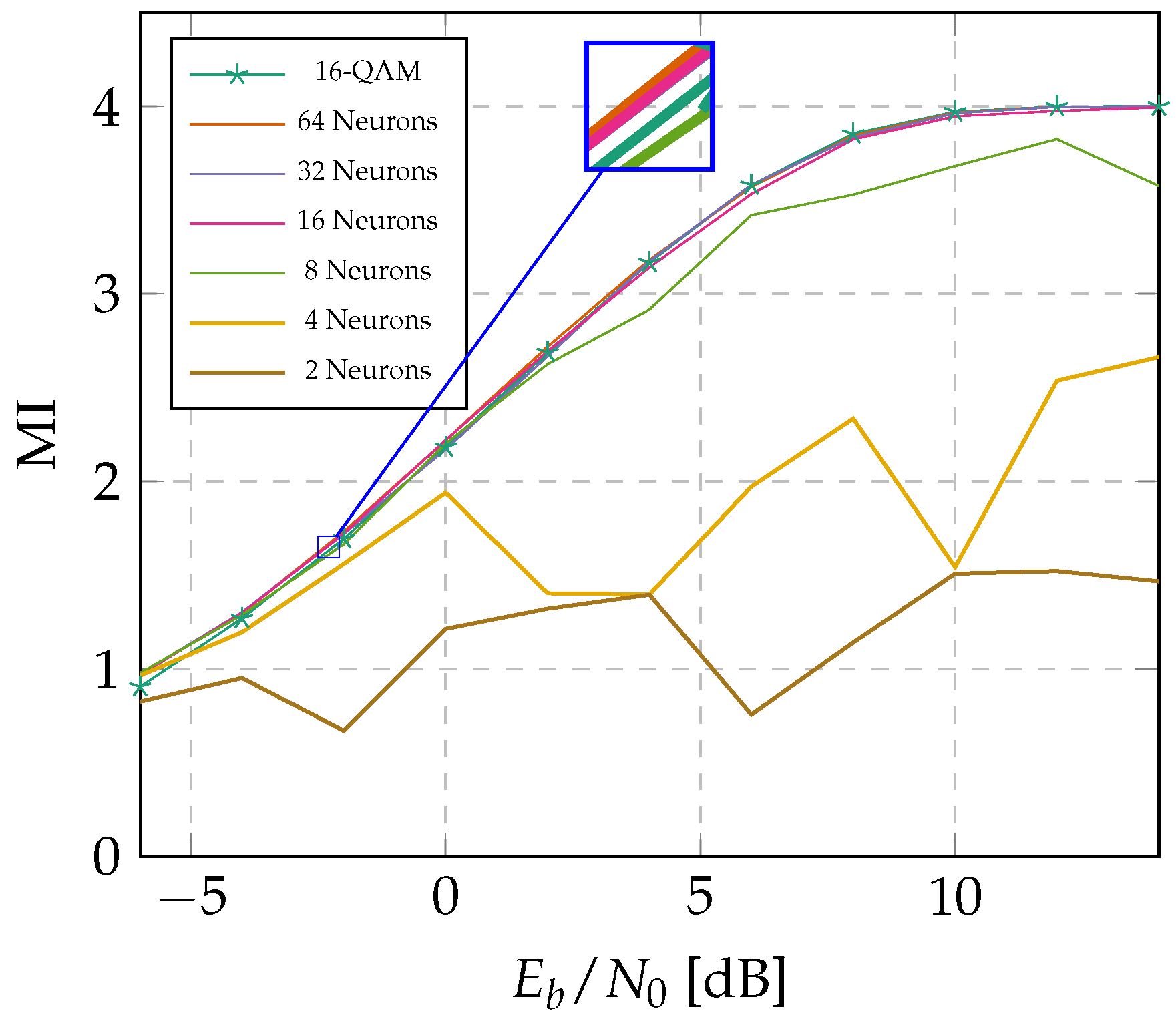
3.3. Topology Optimization Using Cross-Layered Analysis

The number of neurons per layer, denoted by N, is a parameter that affects the communication systems performance (i.e., the MI) and the hardware implementation efficiency (power consumption and latency). Therefore, it is important to select N in a way to optimize the hardware implementation while not degrading the system-level performance. On the one hand, if we focus only on the system performance and forget about the impact of N on the hardware side, we are satisfied as long as N is providing similar bitwise MI as the conventional QAM techniques. On the other hand, if we focus on the hardware implementation, the number of multiply-accumulate (MAC) operations of the ANN grows quadratically with respect to N. Thus, depending on the selected DOP, either the power consumption or the latency will increase.
Since we are adopting a cross-layer approach for our implementation, we aim to select the best model by decreasing the neurons per layer up to the minimum that does not result in degradation of the MI. Therefore, we design a framework that continuously reduces the number of neurons, retrains the network for multiple SNRs and evaluates the bitwise MI for each trained model. Using this approach, we were able to reduce the number of neurons down to N = 16 while keeping the performance stable over the whole SNR range. This way, we can even achieve higher MI compared to 16-QAM for low SNRs while obtaining similar performance for higher SNRs, as show in Figure 3.

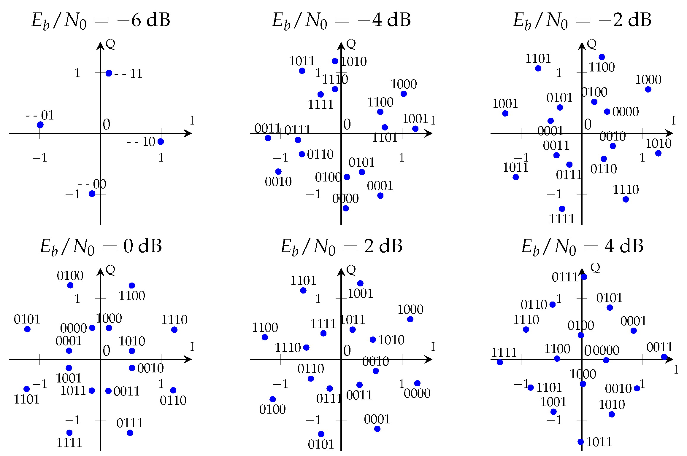
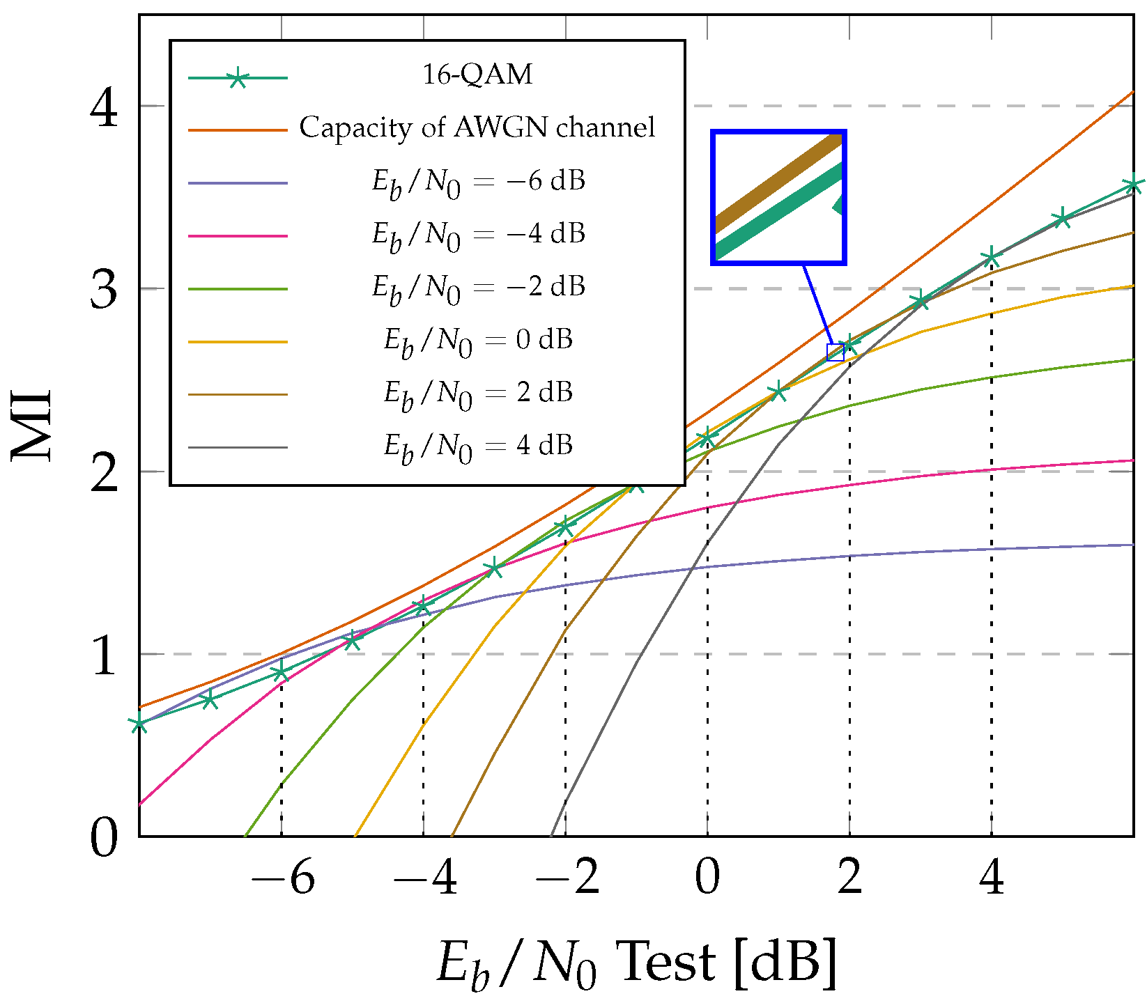
3.4. Training Results

We train the AE shown in Figure 2 in an end-to-end manner through the channel model to minimize the binary cross-entropy loss, which was shown to maximize the bitwise MI [10]. The system is trained for various SNRs to obtain different mapper constellations. As framework for the initial system, we use PyTorch together with the Adam optimizer [33] and AMSgrad [34]. The learning rate is fixed to 0.01 while the training iterations are set to 2000 and 200 for batch size 10,000 and 100,000, respectively. The model is trained for SNRs starting from 6 to 4 dB in steps of two. The resulting constellation diagrams obtained at the mapper’s output are shown in Figure 4. We only trained the model for up to 4 dB as for higher SNR the constellations are similar to 16-QAM.
As can be seen, the higher the SNR the more similar the learned constellation is to a conventional 16-QAM. With lower SNR, the spacing between each point becomes non-uniform, up until multiple messages are mapped to the same symbol for E b / N 0 = 6  dB. This can be explained by the fact that the AE is trained to optimize the bitwise MI; therefore, it increases the reliability for specific bit channels in the low-SNR-region by maximizing the spacing between them, taking into account the information loss for other bit channels that cannot be conveyed reliably at low SNR anyway.
The gain of the AE’s constellations becomes clear when observing the MI as shown in Figure 5. It can be seen that the maximum MI for the given test-SNR is always achieved by the constellation that is also trained for this SNR. The learned constellations consistently outperform the conventional 16-QAM at the SNR they are optimized for. In further analysis, we validate the functionality of our hardware implementation described in Section 4 by reproducing the software results of Figure 5 on FPGA. However, it should be noted that the advantage of the AE compared to conventional systems is not only the gain observed by comparing the MI but primarily the possibility to adapt to varying channel conditions during runtime.

4. Hardware Implementation

In this work, we design an efficient FPGA architecture for the bitwise AE described in Section 3 with focus on low-latency and low-power. To reduce the bandwidth and eliminate the communication overhead of a feedback channel from receiver to transmitter, we fix the constellations of the transmitter after training in software and implement only the receiver as trainable ANN on FPGA. The justification of such a system in terms of communication performance is given in Section 4.1. In summary, the AE system is jointly trained in software but can be fine-tuned and adapted to real channel conditions by re-training the demapper in hardware.

4.1. Reasonability of Demapper Fine-Tuning

As most previous works analyze the communication performance of the complete end-to-end AE system, the question arises how much gain can be achieved by fine-tuning the receiver for channel fluctuations during runtime. In [21], an end-to-end system is trained over an AWGN-based channel model. Afterward, it is tested in a real-world scenario using SDRs in combination with fine-tuning of the receiver. The results show that for over-the-air fine-tuning, it can improve the BLER by up to 1 dB, compared to an AE that is only trained for the channel model. Furthermore, in [35], it is shown that fine-tuning increases the communication performance by up to 1 dB, which can be explained by quantization noise, phase offset, and hardware impairments not considered in the channel model. Those works indicate that the adaption of the receiver to a real channel leads to significant gains and therefore justifies the implementation of a trainable receiver ANN.

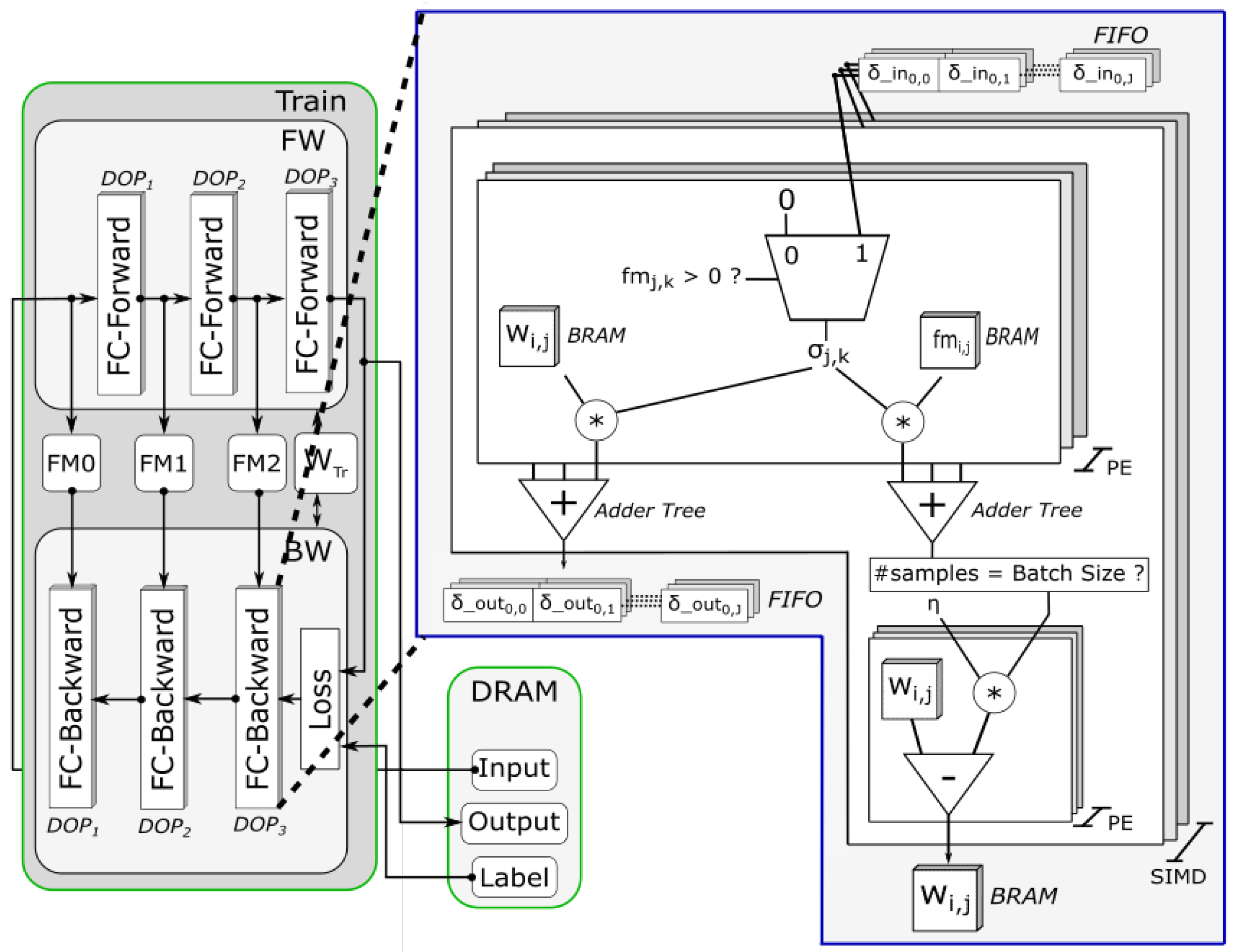
4.2. Hardware Architecture

As a target platform, we choose the Ultra96-V2, as it is low-power, low-cost, and features the Xilinx ZU3EG with 16 nm FinFET technology along with an ARM-Cortex A53 CPU. In the following, we refer to the CPU as processing system (PS) and the ZU3EG FPGA as programmable logic (PL). We use the processing system (PS) to create inputs for the receiver ANN by generating random bit vectors which are mapped to a complex symbol that is determined by the constellation of the trained mapper and propagated over a channel model. Additionally, the PS provides labels for training and calculates the achieved BER and MI. The data are transferred between PS and PL by using the shared dynamic random access memory (DRAM). The hardware design consists of two separate modules for inference and training, respectively. The inference module takes the noisy input message and predicts a corresponding output message, whereas the training module additionally gets the label as input and adjusts the weights using backpropagation and gradient descent. In practice, the labels for retraining are either provided as pilot symbols or by using an outer error correction code (ECC) [36].

4.2.1. Architecture Overview

The look-up tables (LUTs) corresponding to the trained mapper as well as the trainable parameters of the demapper are extracted from the PyTorch design and included in the hardware implementation. In general, both inference and training module are designed as pipelined architecture using Vivado high-level synthesis (HLS) 2019.2 and parts of Xilinx FINN library [37]. Due to the low-complexity, ANN topology with only 388 trainable parameters, all weights can be stored on-chip, resulting in minimal memory overhead and reduced latency. All fully connected layers are implemented as separate hardware modules and operate in a pipelined fashion; thus, a layer can already start its calculation after the first inputs are received. In this way, the overall latency of the complete module is approximately the same as the latency of the slowest layer. The hardware modules for training and inference access the input and output data in DRAM by using memory-mapped AXI interfaces that are internally converted to AXI streams. The DOP can be adjusted for each layer individually to trade-off resource usage against latency. It can be modified by setting the parallelism on a fine-grained level (single instruction multiple data (SIMD)), corresponding to the number of inputs that one neuron calculates in parallel, as well as on a coarse-grained level (processing element (PE)) specifying the number of neurons that are concurrently processed. The DOP can be separately set for the inference and training module to optimally fit the needs of the application and meet the given constraints. To reduce memory resources and computational complexity, we implement all datatypes using a fixed-point format with arbitrary width for fraction and integer part. The integer bit-width for the activations, MAC units, and gradients are adjusted to cover the full range of values, which is determined by simulating 10,000 input samples. The fraction bit-width is set to the minimal value without a loss in accuracy. In particular, the activations are quantized between 11 and 15 bits, the weights to 9 bits, and the gradients to 13 bits.
For the inference module, the input is propagated through the fully connected layers by multiplying with the corresponding weights and adding up the bias to produce the output. As the implementation of ANN-training on FPGA has higher implementation complexity compared to the inference, it is explained in more detail in Section 4.2.2. It is to note that in theory, it is also possible to discard the inference module and use the forward-pass of the training module for inference. In contrast, we have decided to use separate modules for two main reasons:
  • It allows us to set the DOP separately for inference and training module to partition the resources according to the requirements as described in Section 4.3;
  • We are able to operate on a reduced bit-width during inference as compared to training, to save power and energy during inference while keeping high precision during training.

4.2.2. Training Module

The hardware design of the training module is illustrated in Figure 6. As it is shown, it is divided into the forward-pass to calculate the output and the backward-pass to compute the gradient and update the weights. Analogically to the inference module, it operates in a pipelined fashion, starting from the first layer in the forward-pass and from the last layer in the backward-pass. The forward-pass is similar to the inference module with the sole difference that the feature maps between the layers are stored to calculate the gradients during backpropagation. The architecture includes an adjustable batch size, corresponding to the number of samples that are forward-propagated before the update of weights is applied, which is kept very small for the low-latency AE implementation. The backpropagation itself starts by calculating the error term δ j of the loss function depending on the current output a j and the corresponding label y j , as:
δ j = a j y j
Based on this error, the error for each fully connected layer followed by a ReLU layer, up until the first one is calculated, determined by current weight and the error of the following layer, as:
δ j = k σ j , k w i , j with σ j , k = δ j , k if fm j , k 0 0 otherwise
where k corresponds to the following layer’s neuron, j corresponds to the current layer’s neuron and i corresponds to the previous layer’s neuron. This equation is implemented as multiplexer, followed by an adder tree, where parallelization can be adjusted by PE. Based on the error δ j , the weights can be updated as:
Δ w i , j = η k σ j , k fm i , j with σ j , k = δ j , k if fm j , k 0 0 otherwise
where η refers to the learning rate, and fm to the feature map saved by the forward-pass. This is again implemented in hardware using an adder tree. After one batch is processed, all trainable parameters are individually updated by subtracting Δ w i , j from the corresponding weight w i , j . The calculation of the error term δ j and the update of the weights for a fully connected layer followed by a ReLU activation function is depicted on the right side of Figure 6. As shown, the error term is propagated between different layers using FIFOs while the weights are stored in block RAM (BRAM). The weights are partitioned in a way to allow accessing s i m d * p e weights in one clock cycle to not slow down the computation. To allow for different DOP of inference and training module, the weights are transformed corresponding to the partition scheme when exchanged between the modules. In general, the DOP can be calculated as the product of SIMD and PE, referring to input and output parallelism, as shown in Figure 6. In contrast to the inference module, the weights of the training module need to be quantized with up to 14 bits. The main reason for the higher bit-width is that for each training iteration, only a small adaption of the weights is performed; so, higher precision is needed to track this update of the weights. After backpropagation is applied for multiple iterations, the difference becomes significant enough to be also representable by the lower bit-width used during inference. In summary, the novelties of our architecture compared to the related work discussed in Section 2.2 are:
  • Separately adjustable DOPs for inference and train module allow to adapt to application requirements and objectives, which is exploited by our framework as described in Section 4.3;
  • Fully pipelined, on-chip architecture achieves low-latency and high-throughput even for applications that rely on small batch size;
  • Different weight-width for inference and training enables training with higher precision while minimizing resources for inference.

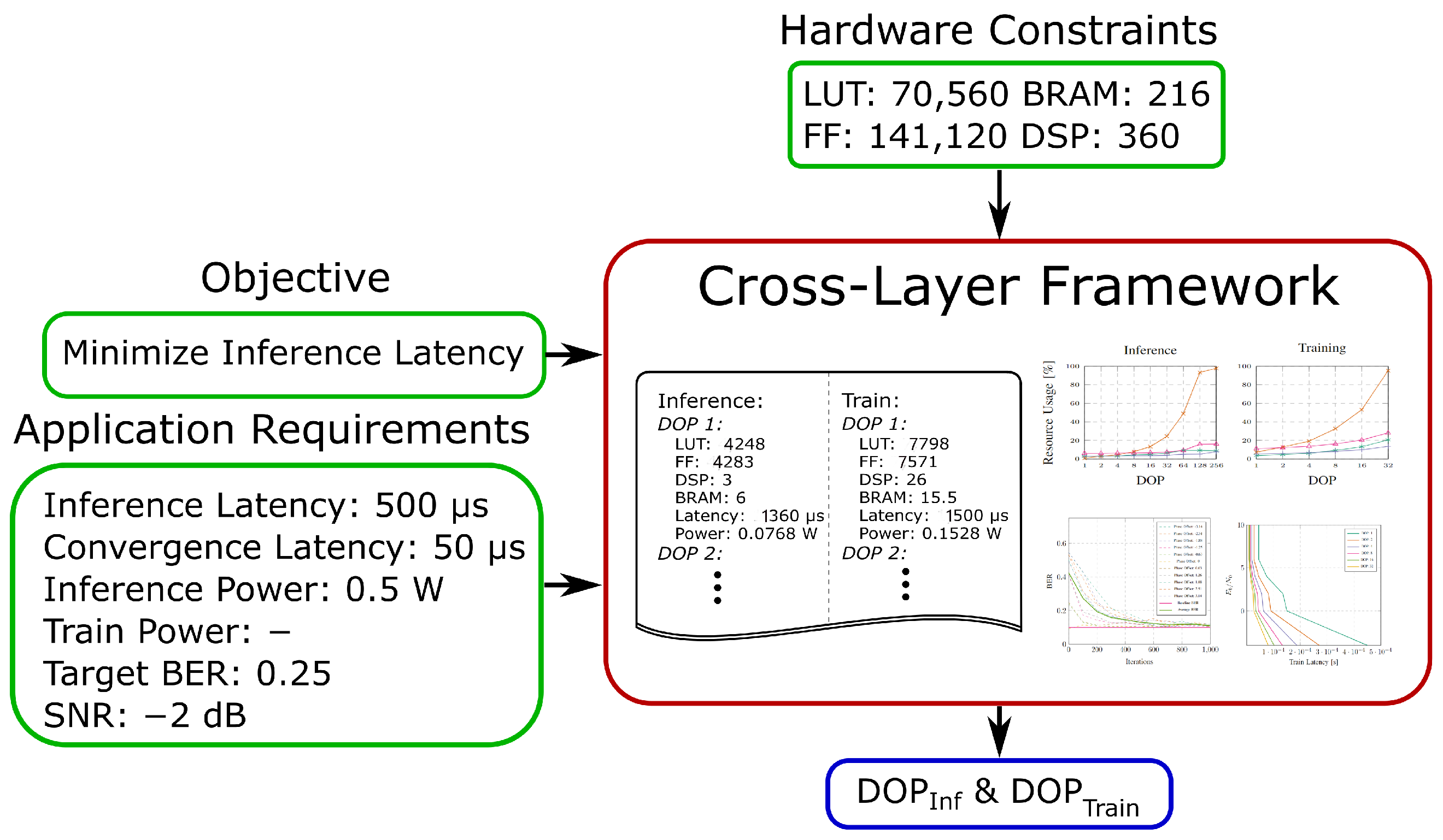
4.3. Cross-Layer Exploration Framework

One of the primary goals of our hardware design is to provide high flexibility, which allows to jointly partition the resources used for inference and training module depending on the environmental conditions (e.g., channel fluctuations) and requirements of the application (e.g., latency, throughput). For example, the frequency of channel variations might increase, therefore faster convergence for the retraining of the network is needed, and the latency of the training module needs to be decreased by utilizing more resources, either through partial reconfiguration or reloading of the bitstream. Theoretically, the reconfiguration of the inference module could even be accomplished without any downtime of the communication by temporally using the resources of the training module as follows:
  • Initial configuration: initial inference module, initial training module;
  • Temporal configuration: initial inference module, new inference module;
  • New configuration: initial training module, new inference module.
To fully exploit the potential of our architecture and to bridge the gap between the communication layer and the hardware layer, we propose a framework that can be executed on the PS of the FPGA to automatically calculate the optimal DOP for inference and training module for requirements such as inference latency or convergence latency for a specific target BER. The pseudo-code implemented in the framework to determine the DOPs is given in Algorithm 1, where R e q ( x ) is defined by the application requirements, and R e s ( x ) of the inference and training module for the different DOPs is obtained by extracting the implementation results for the different configurations from Vivado after place and route.
The objective can either be hardware-related, e.g., minimize power or even take the communication layer into account, e.g., minimize inference latency while satisfying convergence latency requirements for a target BER and an estimated SNR. The algorithm calculates the ideal DOPs by first satisfying the application requirements and afterward optimizing for the given objective under consideration of the available resources given by the hardware constraints.
Using this algorithm, the framework can load the bitstream corresponding to the calculated parallelization degrees during runtime to adapt to the changing requirements.
A sample configuration of the framework for the proposed AE is given in Figure 7.
The framework receives as inputs:
  • The objective, e.g., min. inference latency, min. convergence latency, min. inference power or min. training power;
  • Application requirements in form of latency and power demands and, optionally, a target BER for an estimated SNR;
  • Hardware constraints based on the available resources of the target platform.
Algorithm 1: DOP Calculation.
Electronics 11 01138 i001
The outputs of the framework are the DOPs for the inference and training module that are optimized for the given objective and satisfy the application requirements.
To link the communication-related metrics such as SNR and BER to actual properties of the underlying hardware, the framework internally accesses a database of pre-evaluated characteristics of the hardware modules. Those characteristics include hardware-related properties, such as resource usage, latency and power, as well as a link to the communication layer by mapping different DOPs to convergence times and SNRs, which is further described in Section 5.5.
This way, our design provides two different levels of flexibility:
(1)
Environmental Adaption: The receiver can be fine-tuned to compensate variations of the communication channel by retraining the ANN;
(2)
Requirement Adaption: The FPGA can be reconfigured to satisfy changing application requirements by adapting the DOP of inference and training module.

5. Results and Discussion

In the following, we compare the resource utilization and latency of the inference and training module for multiple DOPs corresponding to different settings of requirements and objectives in our framework. We report the utilization after place and route for the complete inference or training module. The latency is measured on the board for multiple iterations to calculate the average latency for processing one sample. The DOP is increased either until the module is fully parallelized or the requirement cannot be satisfied because the resource limit is reached on the Ultra96-V2. We were able to increase the PL frequency up to 300 MHz without violating timing constraints.

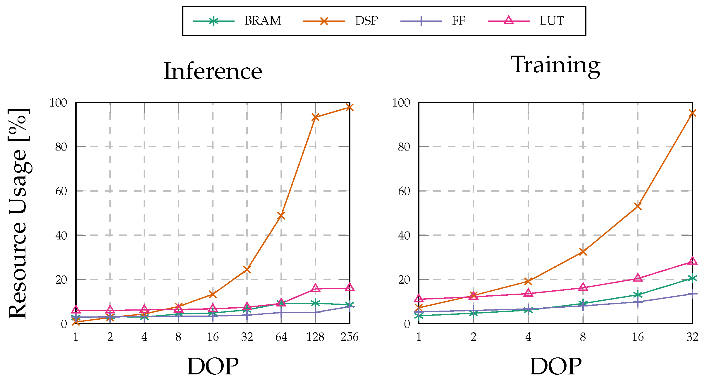
5.1. Resource Utilization
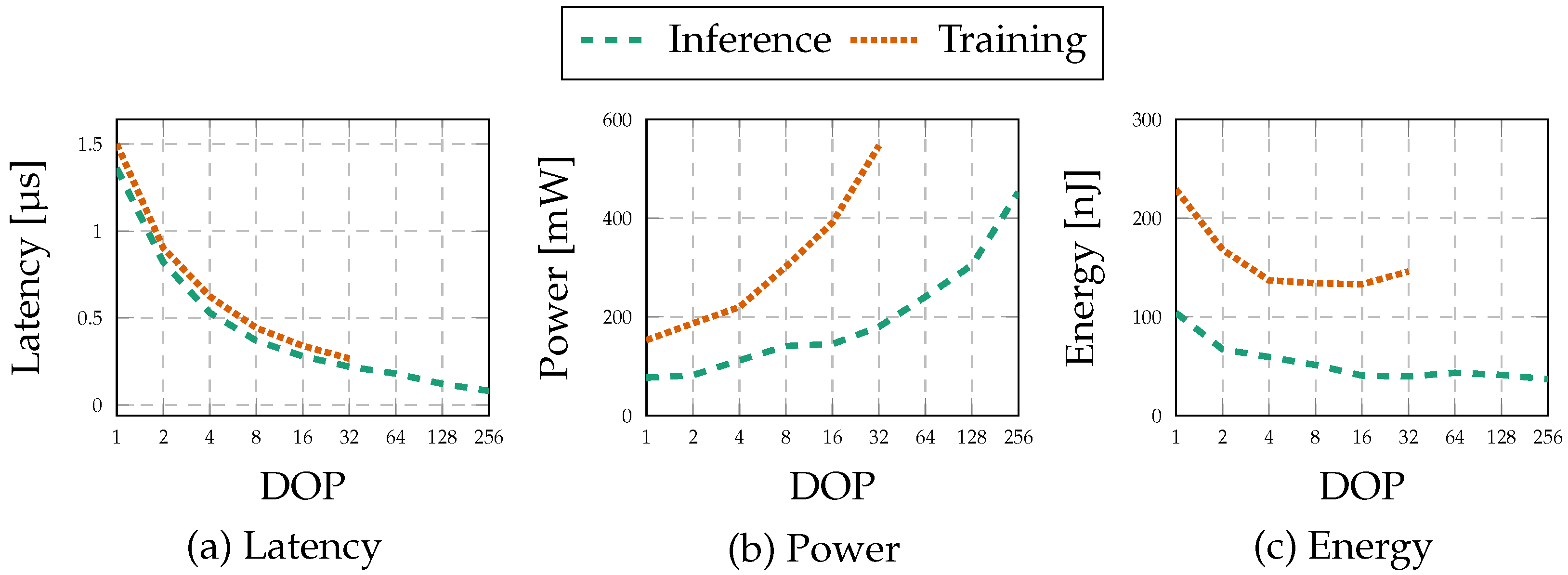
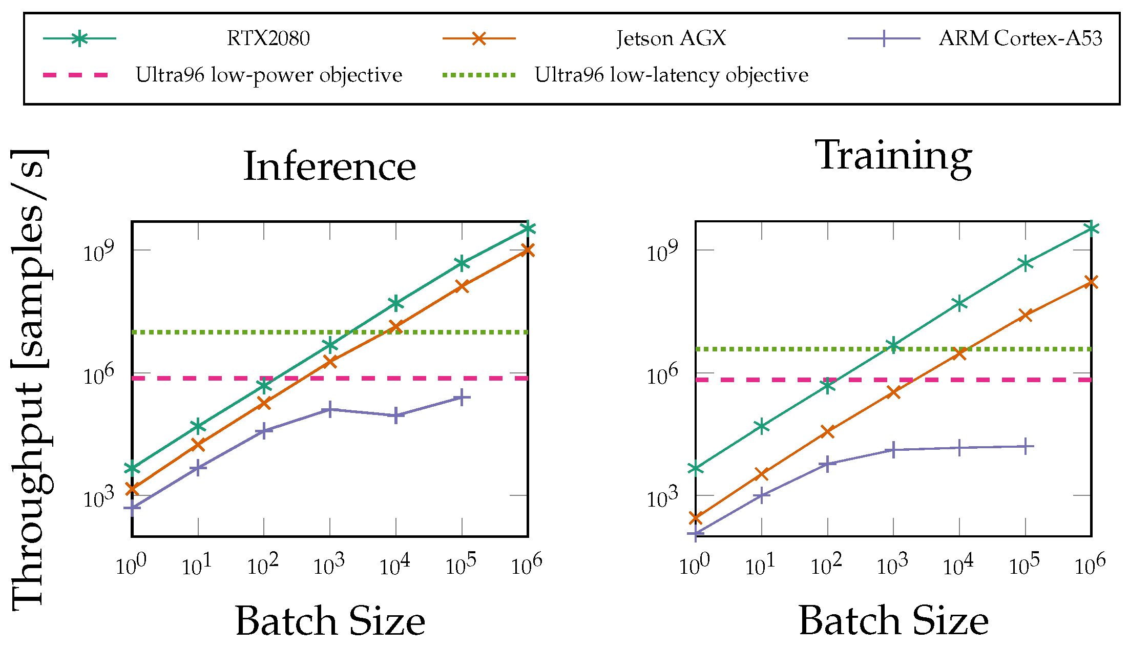
In Figure 8, the resource utilization is shown for DOPs up to 256 for the inference module and 32 for the training module. It can be seen that the resource type with the highest utilization for both modules are digital signal processor (DSP)-units. The inference module can be fully parallelized with a factor of 256, corresponding to the 16 inputs (SIMD) for each of the 16 neurons (PE) of the bottleneck layer.
In contrast, the highest DOP for the training module is 32. If the DOP is further increased, either DSP-units or LUTs exceed the available resources of the board. The higher complexity of this module can primarily be explained by the existence of forward and backward-pass for the training, higher quantization of the weights, and the need to save feature maps for the gradient calculation.
To summarize, it can be seen that it is feasible to implement the inference and training of our ANN with high parallelism even on a low-cost FPGA. Using an FPGA with more available resources would allow for further parallelization, either by increasing the DOP of the training module or by using multiple instances of the modules to increase the throughput.

5.2. Latency

The latency of the two modules for the different DOPs is shown in Figure 9a. For the training module, we report the latency of the backward pass only, as the latency of the forward pass is the same as for the inference module. As expected, the latency decreases with higher DOP up to a minimum of only 81 ns for the inference module and 267 ns for the backward pass. It is to note that the latency does not decrease linearly with the DOP, because, even though the computations of the ANN layers themselves are accelerated, there exists a static component resulting from communication overhead and data transfer between the layers. Additionally, the higher parallelism increases the number of operations of the critical path; thus, Viviado HLS inserts additional registers which increase the latency.
In summary, the latency of our implementation satisfies the constraints of most communication scenarios. For instance, in ultra reliable low-latency communication (uRLLC), end-to-end latencies as low as 5 ms are required. As there are many other, more complex processing blocks in a baseband processing system, the latency overhead of our demapper is negligible, and thus, it could be integrated in such a system without violating the timing constraints.

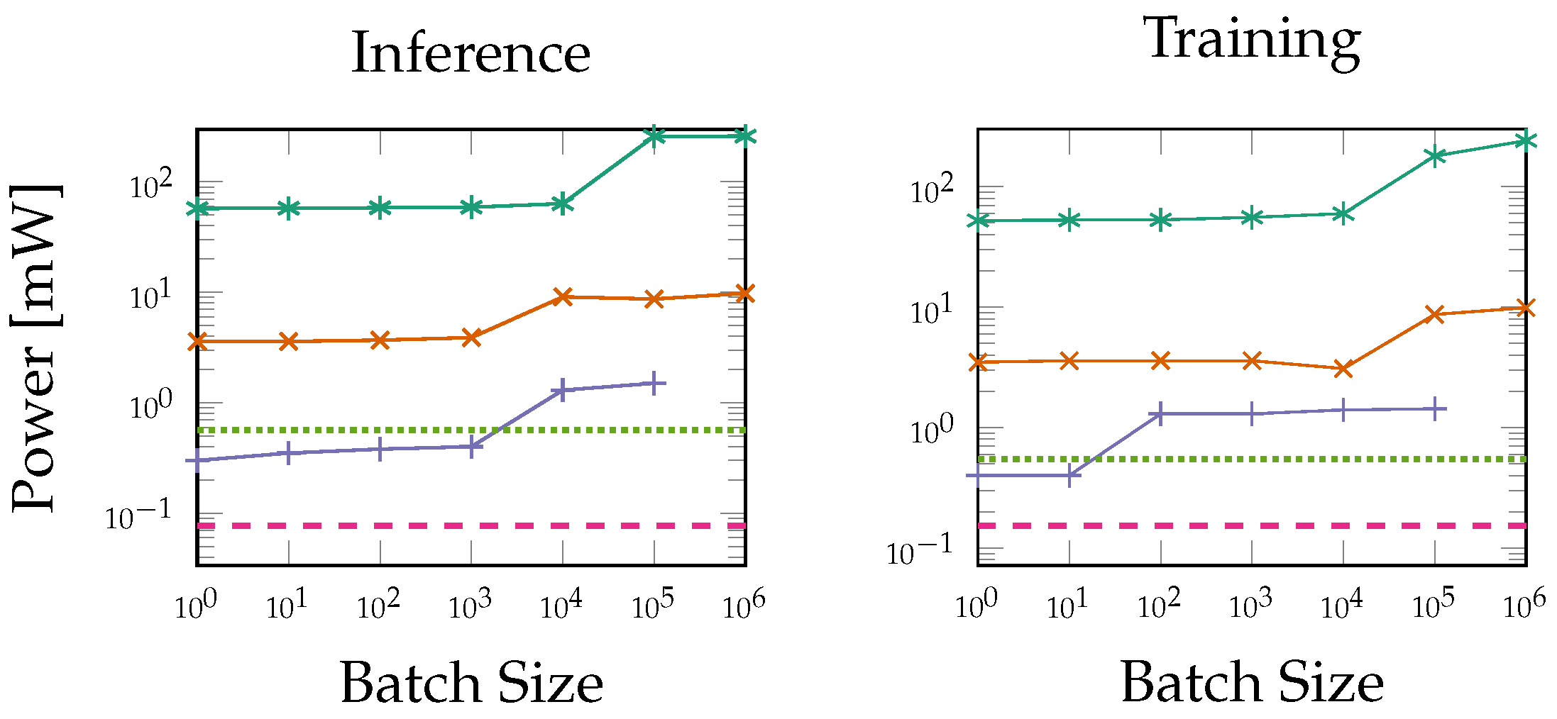
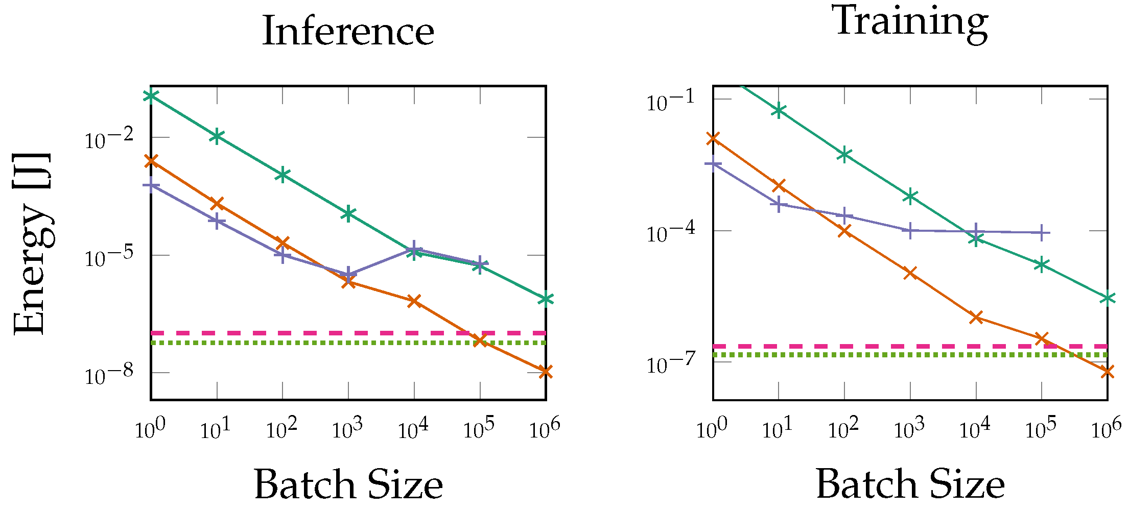
5.3. Power and Energy

To demonstrate the efficiency of our implementation, we measure power and energy for the different DOPs. The power is obtained with the external power meter VOLTCRAFT VC 870. It is measured when the PL is idle as well as during processing of the samples. We report the dynamic power consumption as the difference between idle and processing power. To obtain the energy consumption, we multiply the dynamic power by the average runtime for processing one sample. Figure 9b,c illustrates how the DOP influences the power and energy consumption. In general, the power rises with higher resource utilization, while the energy has fewer deviations because the increasing power consumption is compensated by the lower runtime for high DOPs.
The results illustrated in this section provide the basis for our parallelism exploration framework. Especially the trade-off between low-latency and low-power can be exploited to satisfy the requirements of the application by separately adjusting DOPs for inference and training module. For instance, minimal DOP corresponds to the low-power objective while maximal DOP corresponds to low-latency.
All in all, the presented analysis demonstrates the high flexibility and efficiency of our design. This flexibility is shown in terms of resource requirements and regarding the latency, power and energy trade-off. This is highly important for our application as it provides a solution to adapt to the different requirements introduced by the variety of baseband processing systems and it shows that our solution is not only optimized for one specific use-case.

5.4. Performance Demonstration

To demonstrate the performance of our AE implementation, we show how the receiver can adapt to a varying phase offset of the channel. Therefore, we train the AE for a standard AWGN channel with zero phase-offset. Afterward, the trainable receiver is implemented in hardware, and we modify the channel conditions by changing the phase offset of the channel model by drawing from a uniform distribution from π to π for an E b / N 0 of 2 dB. Subsequently, fine-tuning of the receiver is applied by retraining for the new channel characteristics. It is to note that phase offset is a simple example of the adaptability of our architecture; in theory, it can also adapt to more complex channel fluctuations which will be further explored in future work. Figure 10 shows the convergence of the demapper ANN for the described scenario, including the BERs of the different phase offsets, the average BER and the baseline BER corresponding to an AWGN channel without phase offset.
It can be seen that for all phase offsets, the BER of the demapper ANN converges to that of the baseline. The convergence process is nonlinear, the gain is the highest for the first iterations and it decreases during the training. For instance, the average BER is reduced by a factor of 2.2 during the first 200 iterations. For small phase offsets of ± 0.63 , 200 iterations are even enough to approach the baseline BER. Figure 10 provides a first step towards connecting the communication layer to the hardware layer which will be described in more detail in Section 5.5.
In Figure 11, the average BER of the training process for multiple phase offsets is plotted over different SNRs for various number of training iterations. This illustrates how the convergence varies for different SNRs.
The gap between the baseline AWGN channel and the average BER of the phase offset channel is fairly small for low SNRs after training for an appropriate number of iterations. This gap increases for larger SNRs. The behavior can be explained by the fact that for high SNRs, the target BER is much lower, and therefore, small fluctuations of the learned decision regions (DRs) from the optimal ones are directly reflected in the BER. This problem can be solved by reducing the learning rate of the AE for higher SNRs with the drawback of an increased convergence time.
It is worth mentioning that in Figure 11, we do not intend to show the communication performance on the system-level. Since our work focuses on the implementation of the trainable demapper, we are evaluating the performance of this block, without including post-processing steps (channel decoding and soft-decisions) that are necessary to improve the BER of the overall system. As shown, with higher number of iterations, we are getting the same performance as the conventional technique. However, the main goal at this stage is to have a deeper look at the interrelations between the different layer’s parameters, i.e., the number of iterations needed for convergence with respect to a system performance metric which is the BER in our case for different SNRs.

5.5. Interaction of Design Layers

The proposed work of designing an FPGA-based AE for communication can be divided into three main design layers: communication systems, ANN design and hardware implementation. Those layers are not independent but highly influence each other; therefore, a joint analysis is of high importance for efficient cross-layer design. We go one step further towards this design methodology as shown in Figure 12, by relating metrics of all design layers: SNR (communication layer), training latency (ANN design layer, hardware implementation layer) and DOP (hardware implementation layer).
Figure 12 shows the training latency needed to reach a target BER of 0.25 over different SNRs for multiple DOPs. The latency to obtain the target BER increases with lower DOP and lower SNR. With higher SNRs, the number of iterations needed to get to a target BER will be reduced. Therefore, we can see in Figure 12 that for any given DOP, higher E b / N 0 reduces the training latency for the fine-tuning. Nevertheless, this latency reduction is not linear and is dependent on the DOP used. By having a closer look at the region when the E b / N 0 is smaller than 0 dB, the training latency for the fine-tuning increases exponentially when the DOP is reduced from 32 to 1. The difference in latency between different DOPs decreases for higher E b / N 0 regimes (from 0 to 5 dB) and becomes much smaller in the regime when E b / N 0 is between 5 dB and 10 dB. For E b / N 0 higher than 6 dB, the increase in the DOP from 8 to 32 brings negligible improvement in terms of latency. Therefore, whenever communicating in high SNR regimes, we can simply release the adopted DOP on hardware to reduce the power consumption, since keeping high DOP configuration will not bring improvement on the ANN performance in terms of the latency reduction. However, when operating in low SNR regimes, it is very critical to increase the DOP on hardware because this will reduce the training latency more than 5 times as seen at –5 dB when going from DOP = 1 to 32.
The data visualized in Figure 12 are also one main building block of our cross-layer framework. Based on those evaluations, the framework is able to calculate the optimal DOPs for the application constraints such as target BER and training latency.

6. Comparison

6.1. Comparison to State of the Art FPGA-Based Training

As discussed in Section 2.2, there already exist some frameworks to efficiently map the ANN training flow to FPGA. The hardware metrics of the presented works are shown in Table 1. From the shown results, we can directly tell that [22,23,29,30] target applications, where the main focus is to increase the throughput of the accelerator, result in high dynamic power consumption. This would violate the requirements of our application, because many communication algorithms are implemented on power-constrained embedded systems with limited energy budget, such as smartphones or internet of things (IoT) devices. The only related work that could satisfy the constraints of our application is [31]. Although its focus is on CNNs while our ANN architecture is based on fully-connected layers, it is still comparable to our approach as it targets low-latency and low-power. Based on the presented results, they report higher power consumption (0.67 compared to 0.568 W), lower throughput (4.39 compared to 5.28 GOPS) and 67% lower energy efficiency compared to our approach.

6.2. FPGA Performance Compared to General-Purpose Processors

To demonstrate the advantage of our FPGA design, we compare our implementation to the same network executed on general-purpose processors. As target platforms, we choose the high-performance GPU Nvidia RTX 2080, the embedded GPU Nvidia Jetson AGX and the embedded CPU ARM Cortex-A53. For a fair comparison, we implement only the decoder part of the AE on the general-purpose processors in a PyTorch environment. We compare throughput, energy efficiency and power consumption for inference and training. In contrast to our FPGA architecture, the throughput of those platforms increases dramatically with higher batch size; thus, we increase the batch size up until the device runs out of memory. It is to note that for the application of demapping communication symbols in low-latency communication, such high batch sizes are not practical, because the data enter the system sequentially and waiting for a complete batch would result in high latencies. However, for the sake of completeness and to give a baseline for other use cases, we also provide results for high batch sizes.
Figure 13 shows the throughput of the high-performance GPU, embedded GPU, and embedded CPU compared to the power- and latency-optimized FPGA implementation. For a batch size of one, the throughput of the ARM Cortex-A53 is 495 samples/s for inference and 118 samples/s for backpropagation. The graphics processor units (GPUs) Jeston AGX and Nvidia RTX 2080 achieve 1450 and 4670 samples/s for inference as well as 282 and 978 samples/s for training. In contrast, the FPGA outperforms the high-performance GPU for very small batch sizes with 1.23 · 10 7 samples/s for inference and 3.75 · 10 6 samples/s for backpropagation by a factor of 2000 and 3800, respectively. The high parallelism of the RTX 2080 is only exploited with increasing batch size and leads to higher throughput than the FPGA starting from batch size 10,000, which is far from being practical for low-latency communication systems.
The power measurements are based on nvidia-smi for the graphics processor units (GPUs) and obtained with an external power meter for the CPU. Similar to the FPGA, the idle power is subtracted from the processing power to compute the dynamic power consumption. As shown in Figure 14, the FPGA consumes between 0.077 W and 0.568 W of power, whereas the high-performance GPU draws up to 259 W and the embedded GPU up to 9.8 W. Only the embedded CPU’s power consumption lies in the same order of magnitude as the FPGA’s, with 0.4 to 1.4 W.
The dynamic energy consumption is calculated as the product of dynamic power and the average runtime of one sample. As illustrated in Figure 15, the FPGA outperforms all other platforms up to batch size 100,000, where only the Nvidia Jetson AGX is more energy efficient. For very small batch sizes, there is a huge gap between the Ultra96 and all other platforms. It consumes around 5000 times less energy than the embedded CPU.
Those results show that general-purpose processors do not always provide an optimal platform for the inference and training of ANNs. In contrast to central processing units (CPUs) and graphics processor units (GPUs), the flexibility of FPGAs enables a high level of specialization, because the DOP can be adapted to the constraints and requirements, which is exploited by our framework. Especially in the case of energy-constrained embedded devices or in applications where data arrive sequentially and processing in large batches is not possible, FPGAs provide outstanding performance in terms of latency, power consumption, and energy efficiency.

6.3. ANN Solution vs. Conventional Systems

Currently, the practical application of machine learning algorithms in the area of communication systems is fairly low. To analyze if there is potential of the ANN-based AE to replace highly-optimized traditional communication algorithms and to show pros and cons, we provide a short discussion in the following.
Therefore, we implement the suboptimal soft-demapping algorithm proposed in [38] which replaces exponential and logarithmic functions by simplified calculations according to:
l l r ( b k | s r ) = 1 2 σ 2 . min i ( s r c i , k = 0 ) 2 min i ( s r c i , k = 1 ) 2
where b k is the k-th bit, s r is the received symbol and c i , k = 0 and c i , k = 1 represent the constellation symbols whose k-th bits are ‘0’ and ‘1’, respectively. A comparison to the ANN-based demapper is given in Table 2.
By comparing the conventional soft-demapper implementation to the AE-based solutions, it becomes clear that the implementation complexity of a conventional demapper on FPGA is much lower compared to a system based on ANNs. Nevertheless, the results show that the AE can achieve comparable performance when optimized for the respective metric. The latency-optimized AE implementation achieves a latency in the same order of magnitude as the conventional soft-demapper. The same applies to the power-optimized AE when comparing its power consumption to that of the soft-demapper. However, the throughput of the soft-demapper is much higher compared to the AE and it could even be increased further by instantiating multiple modules in parallel, which is possible due to the low resource utilization. This shows that FPGA implementations of ANN-based systems currently lag behind highly-optimized traditional systems in terms of implementation complexity when considering the demapping only. Nevertheless, various works demonstrated that an AE-based system is able to also perform much more complex tasks of the communication chain. For example, the authors of [39] showed that a small ANN of only two convolutional layers is able to perform blind channel equalization. Moreover, the authors of [40] demonstrated that even a complex Wiener filter can be outperformed by an ANN-based approach. Those results show that also more complex communication tasks can be fulfilled by an end-to-end AE system, which might result in a more competitive hardware implementation as further processing blocks are implicitly included in the AE. Additionally, end-to-end trainable systems have advantages in specific application scenarios for multiple reasons. To build a traditional communication system for a real-world scenario, it is essential to have a channel model that represents the real channel as close as possible. If there are large deviations between generic model and reality, the performance of the system suffers dramatically in certain conditions. In addition, even if the channel is known precisely, adjusting the parameters of the different communication blocks requires much development time and the knowledge of a communication expert. In contrast, an end-to-end trainable system does not need detailed information about the underlying channel but is able to correct deviations of the model by fine-tuning during runtime. Moreover, an extensive parameter search is not necessary, as it is implicitly included in the training of the network.

7. Conclusions

We have presented a hardware architecture of an AE-based communication system that is able to fine-tune for channel fluctuations in the form of phase offset variations, by retraining the receiver-ANN during runtime. Our FPGA implementation is ideally suited for low-power and low-latency communication scenarios as it operates on a small batch size and is designed as a pipelined on-chip architecture. Additionally, the design is highly flexible as it supports variable quantization and a DOP that can be configured individually for inference and training. Furthermore, we propose a framework that bridges the gap between the communication system layer and the hardware layer by adjusting the DOP depending on application requirements and hardware constraints. We have demonstrated the advantages of our hardware architecture and FPGA as an implementation platform by comparing it to different general-purpose processors. As a result our FPGA-based AE implementation achieves 2000× higher throughput than a high-performance GPU, draws 5× less power than an embedded CPU, and is 5800× more energy efficient compared to an embedded GPU, for small batch size.

8. Future Work

We believe that the presented work is not only about the ability to efficiently implement an ANN topology for a communication system on an FPGA, but rather, it is an actual step towards bridging the gap between the communication system layer and the hardware implementation layer for ANN-based designs. There are still many challenges to tackle in terms of system performance improvement, ANN optimization, and efficient hardware implementation. However, we believe that providing a cross-layer analysis approach is critical for any research advancement towards implementable algorithms.
At the communication system layer, the future work will include modeling real non-static channels that vary with time and evaluate how it affects the performance of the trainable demapper. In addition, an adaptable constellation scheme based on the channel state could be developed to improve the performance of the system. On the ANN layer, there are further possibilities to improve the selection of hyperparameters (number of layers, type of the neurons, etc.). On the hardware layer, future research could focus on the adaptation of resources in a feedback loop to drive the system automatically and dynamically towards optimal implementations. This future work should be studied again in a cross-layer approach to increase the understanding of the impact of each layer on other layers and to show their hidden interdependencies.

Author Contributions

Funding acquisition, S.t.B. and N.W.; investigation, B.H.; methodology, B.H., S.D., M.H. and J.C.; project administration, M.H., S.t.B. and N.W.; software, J.N.; Supervision, S.t.B. and N.W.; validation, J.N. and S.D.; writing—original draft, J.N., S.D. and J.C.; writing—review and editing, B.H., M.H., S.t.B. and N.W. All authors have read and agreed to the published version of the manuscript.

Funding

This work was partly funded by the German ministry of education and research (BMBF) under grant 16KIS1185 (FunKI) and under grand 16KISK004 (Open6GHuB).

Conflicts of Interest

The authors declare no conflict of interest.

References

  1. Zehavi, E. 8-PSK trellis codes for a Rayleigh channel. IEEE Trans. Commun. 1992, 40, 873–884. [Google Scholar] [CrossRef]
  2. Sethuraman, T.; Elias, S.; Ashok, A. A Machine Learning based M-ary Amplitude Modulated Visible Light Communication System. In Proceedings of the 2020 International Conference on COMmunication Systems & NETworkS (COMSNETS), Bengaluru, India, 7–11 January 2020; pp. 694–695. [Google Scholar]
  3. Gao, B.; Bu, B.; Zhang, W.; Li, X. An Intrusion Detection Method Based on Machine Learning and State Observer for Train-Ground Communication Systems. IEEE Trans. Intell. Transp. Syst. 2021, 1–13. [Google Scholar] [CrossRef]
  4. Mahmood, M.R.; Matin, M.A. A Design of Extreme Learning Machine Based Receiver for 2 × 2 MIMO-OFDM System. In Proceedings of the 2021 IEEE International Conference on Communication, Networks and Satellite (COMNETSAT), Purwokerto, Indonesia, 17–18 July 2021; pp. 367–370. [Google Scholar]
  5. Kim, H.; Moon, S.; Hwang, I. Machine Learning-based Channel Tracking for Next-Generation 5G Communication System. In Proceedings of the 2021 Twelfth International Conference on Ubiquitous and Future Networks (ICUFN), Jeju Island, Korea, 17–20 August 2021; pp. 267–269. [Google Scholar]
  6. O’Shea, T.; Hoydis, J. An Introduction to Deep Learning for the Physical Layer. IEEE Trans. Cogn. Commun. Netw. 2017, 3, 563–575. [Google Scholar] [CrossRef] [Green Version]
  7. Karanov, B.; Chagnon, M.; Thouin, F.; Eriksson, T.A.; Bulow, H.; Lavery, D.; Bayvel, P.; Schmalen, L. End-to-End Deep Learning of Optical Fiber Communications. J. Light. Technol. 2018, 36, 4843–4855. [Google Scholar] [CrossRef]
  8. Zhu, Z.R.; Zhang, J.; Chen, R.H.; Yu, H.Y. Autoencoder-Based Transceiver Design for OWC Systems in Log-Normal Fading Channel. IEEE Photonics J. 2019, 11, 1–12. [Google Scholar] [CrossRef]
  9. Mohamed, S.; Dong, J.; Junejo, A.R.; Zuo, D.C. Model-Based: End-to-End Molecular Communication System Through Deep Reinforcement Learning Auto Encoder. IEEE Access 2019, 7, 70279–70286. [Google Scholar] [CrossRef]
  10. Cammerer, S.; Aoudia, F.A.; Dörner, S.; Stark, M.; Hoydis, J.; ten Brink, S. Trainable Communication Systems: Concepts and Prototype. IEEE Trans. Commun. 2020, 68, 5489–5503. [Google Scholar] [CrossRef]
  11. Ibnkahla, M. Applications of neural networks to digital communications—A survey. Signal Process. 2000, 80, 1185–1215. [Google Scholar] [CrossRef]
  12. Bkassiny, M.; Li, Y.; Jayaweera, S.K. A survey on machine-learning techniques in cognitive radios. IEEE Commun. Surv. Tutor. 2012, 15, 1136–1159. [Google Scholar] [CrossRef]
  13. Zorzi, M.; Zanella, A.; Testolin, A.; De Grazia, M.D.F.; Zorzi, M. Cognition-based networks: A new perspective on network optimization using learning and distributed intelligence. IEEE Access 2015, 3, 1512–1530. [Google Scholar] [CrossRef]
  14. Kim, M.; Kim, N.I.; Lee, W.; Cho, D.H. Deep learning-aided SCMA. IEEE Commun. Lett. 2018, 22, 720–723. [Google Scholar] [CrossRef]
  15. Karanov, B.; Liga, G.; Aref, V.; Lavery, D.; Bayvel, P.; Schmalen, L. Deep learning for communication over dispersive nonlinear channels: Performance and comparison with classical digital signal processing. In Proceedings of the 2019 57th Annual Allerton Conference on Communication, Control, and Computing (Allerton), Monticello, IL, USA, 24–27 September 2019; pp. 192–199. [Google Scholar]
  16. Umuroglu, Y.; Fraser, N.J.; Gambardella, G.; Blott, M.; Leong, P.; Jahre, M.; Vissers, K. FINN: A Framework for Fast, Scalable Binarized Neural Network Inference. In Proceedings of the 2017 ACM/SIGDA International Symposium on Field-Programmable Gate Arrays, Monterey, CA, USA, 22–24 February 2017; pp. 65–74. [Google Scholar] [CrossRef] [Green Version]
  17. Zhang, X.; Wang, J.; Zhu, C.; Lin, Y.; Xiong, J.; Hwu, W.m.; Chen, D. DNNBuilder: An Automated Tool for Building High-Performance DNN Hardware Accelerators for FPGAs. In Proceedings of the 2018 IEEE/ACM International Conference on Computer-Aided Design (ICCAD), San Diego, CA, USA, 5–8 November 2018; pp. 1–8. [Google Scholar] [CrossRef]
  18. Fahim, F.; Hawks, B.; Herwig, C.; Hirschauer, J.; Jindariani, S.; Tran, N.; Carloni, L.P.; Guglielmo, G.D.; Harris, P.C.; Krupa, J.D.; et al. hls4ml: An Open-Source Codesign Workflow to Empower Scientific Low-Power Machine Learning Devices. arXiv 2021, arXiv:2103.05579. [Google Scholar]
  19. Goodfellow, I.; Bengio, Y.; Courville, A. Deep Learning; MIT Press: Cambridge, MA, USA, 2016; Available online: http://www.deeplearningbook.org (accessed on 23 February 2022).
  20. Alberge, F. Deep Learning Constellation Design for the AWGN Channel with Additive Radar Interference. IEEE Trans. Commun. 2019, 67, 1413–1423. [Google Scholar] [CrossRef] [Green Version]
  21. Dörner, S.; Cammerer, S.; Hoydis, J.; ten Brink, S. Deep Learning Based Communication Over the Air. IEEE J. Sel. Top. Signal Process. 2018, 12, 132–143. [Google Scholar] [CrossRef] [Green Version]
  22. Geng, T.; Wang, T.; Sanaullah, A.; Yang, C.; Xu, R.; Patel, R.; Herbordt, M. FPDeep: Acceleration and Load Balancing of CNN Training on FPGA Clusters. In Proceedings of the 2018 IEEE 26th Annual International Symposium on Field-Programmable Custom Computing Machines (FCCM), Boulder, CO, USA, 29 April–1 May 2018; pp. 81–84. [Google Scholar] [CrossRef]
  23. Luo, C.; Sit, M.K.; Fan, H.; Liu, S.; Luk, W.; Guo, C. Towards efficient deep neural network training by FPGA-based batch-level parallelism. J. Semicond. 2020, 41, 022403. [Google Scholar] [CrossRef]
  24. Nakahara, H.; Sada, Y.; Shimoda, M.; Sayama, K.; Jinguji, A.; Sato, S. FPGA-based Training Accelerator Utilizing Sparseness of Convolutional Neural Network. In Proceedings of the 2019 29th International Conference on Field Programmable Logic and Applications (FPL), Barcelona, Spain, 8–12 September 2019; pp. 180–186. [Google Scholar] [CrossRef]
  25. Krizhevsky, A.; Sutskever, I.; Hinton, G.E. ImageNet Classification with Deep Convolutional Neural Networks; Advances in Neural Information Processing Systems; Pereira, F., Burges, C.J.C., Bottou, L., Weinberger, K.Q., Eds.; Curran Associates, Inc.: Red Hook, NY, USA, 2012; Volume 25. [Google Scholar]
  26. Simonyan, K.; Zisserman, A. Very Deep Convolutional Networks for Large-Scale Image Recognition. arXiv 2014, arXiv:1409.1556. [Google Scholar]
  27. Howard, A.G.; Zhu, M.; Chen, B.; Kalenichenko, D.; Wang, W.; Weyand, T.; Andreetto, M.; Adam, H. MobileNets: Efficient Convolutional Neural Networks for Mobile Vision Applications. arXiv 2017, arXiv:1704.04861. [Google Scholar]
  28. Di Cecco, R.; Sun, L.; Chow, P. FPGA-based training of convolutional neural networks with a reduced precision floating-point library. In Proceedings of the 2017 International Conference on Field Programmable Technology (ICFPT), Melbourne, Australia, 11–13 December 2017; pp. 239–242. [Google Scholar] [CrossRef]
  29. Liu, Z.; Dou, Y.; Jiang, J.; Wang, Q.; Chow, P. An FPGA-based processor for training convolutional neural networks. In Proceedings of the 2017 International Conference on Field Programmable Technology (ICFPT), Melbourne, Australia, 11–13 December 2017; pp. 207–210. [Google Scholar] [CrossRef]
  30. Venkataramanaiah, S.K.; Ma, Y.; Yin, S.; Nurvitadhi, E.; Dasu, A.; Cao, Y.; Seo, J. Automatic Compiler Based FPGA Accelerator for CNN Training. arXiv 2019, arXiv:1908.06724. [Google Scholar]
  31. Hong, J.; Arslan, S.; Lee, T.; Kim, H. Design of Power-Efficient Training Accelerator for Convolution Neural Networks. Electronics 2021, 10, 787. [Google Scholar] [CrossRef]
  32. Böcherer, G. Achievable Rates for Probabilistic Shaping. arXiv 2017, arXiv:1707.01134. [Google Scholar]
  33. Kingma, D.P.; Ba, J. Adam: A Method for Stochastic Optimization. In Proceedings of the 3rd International Conference on Learning Representations, ICLR 2015, San Diego, CA, USA, 7–9 May 2015. [Google Scholar]
  34. Reddi, S.J.; Kale, S.; Kumar, S. On the Convergence of Adam and Beyond. arXiv 2019, arXiv:1904.09237. [Google Scholar]
  35. Dörner, S.; Henninger, M.; Cammerer, S.; ten Brink, S. WGAN-based Autoencoder Training Over-the-air. arXiv 2020, arXiv:2003.02744. [Google Scholar]
  36. Schibisch, S.; Cammerer, S.; Dörner, S.; Hoydis, J.; ten Brink, S. Online Label Recovery for Deep Learning-based Communication through Error Correcting Codes. arXiv 2018, arXiv:1807.00747. [Google Scholar]
  37. Labs, X.R. FINN HLS Library. Available online: https://github.com/Xilinx/finn-hlslib (accessed on 22 January 2022).
  38. Robertson, P.; Villebrun, E.; Hoeher, P. A comparison of optimal and sub-optimal MAP decoding algorithms operating in the log domain. In Proceedings of the IEEE International Conference on Communications ICC ’95, Seattle, WA, USA, 18–22 June 1995; Volume 2, pp. 1009–1013. [Google Scholar] [CrossRef]
  39. Caciularu, A.; Burshtein, D. Blind Channel Equalization using Variational Autoencoders. arXiv 2018, arXiv:1803.01526. [Google Scholar]
  40. Fischer, M.B.; Dörner, S.; Cammerer, S.; Shimizu, T.; Cheng, B.; Lu, H.; ten Brink, S. Wiener Filter versus Recurrent Neural Network-based 2D-Channel Estimation for V2X Communications. arXiv 2021, arXiv:2102.03163. [Google Scholar]
Figure 1. Digital communication chain.
Electronics 11 01138 g001
Figure 2. Overview of the AE ANN structure.
Electronics 11 01138 g002
Figure 3. ANN topology optimization for different number of neurons compared to 16-QAM.
Electronics 11 01138 g003
Figure 4. Constellations learned by autoencoder for 4 bits per symbol.
Electronics 11 01138 g004
Figure 5. MI of autoencoder constellations compared to channel capacity and 16-QAM.
Electronics 11 01138 g005
Figure 6. FPGA design of the training module.
Electronics 11 01138 g006
Figure 7. Exploration Framework.
Electronics 11 01138 g007
Figure 8. Resource utilization on Ultra96-V2.
Electronics 11 01138 g008
Figure 9. Latency, power and energy on Ultra96-V2.
Electronics 11 01138 g009
Figure 10. Convergence of phase offset for E b / N 0 = 2 .
Electronics 11 01138 g010
Figure 11. BER over SNR for different number of training iterations.
Electronics 11 01138 g011
Figure 12. Influence of DOP on convergence latency for a target BER of 0.25.
Electronics 11 01138 g012
Figure 13. Throughput comparison.
Electronics 11 01138 g013
Figure 14. Power comparison.
Electronics 11 01138 g014
Figure 15. Energy comparison.
Electronics 11 01138 g015
Table 1. Comparison to state-of-the-art FPGA training frameworks.
Batch
Size
Power
[W]
Throughput
[GOPS]
Efficiency
[GOPS/W]
[22]12824.7122038.13
[23]12812.4276.722.3
[29]1614.2486.126.05
[30]4050.54799.49
[31]10.674.396.55
Ours10.5685.289.656
Table 2. Comparison of AE-based inference to conventional soft demapping.
BRAMDSPFFLUTLatency
[s]
Throughput
[bit/s]
Power
[W]
AE low-power objective63428342481.36 · 10 6 2.94 · 10 6 7.68 · 10 2
AE low-latency objective18.535210,89511,3438.10 · 10 8 4.92 · 10 7 4.53 · 10 1
Conventional demapper01104211075.33 · 10 8 3.00 · 10 8 5.5 · 10 2
Publisher’s Note: MDPI stays neutral with regard to jurisdictional claims in published maps and institutional affiliations.

