1. Introduction
DC-DC converters are widely used in various electronic systems because of their high conversion efficiency, low power dissipation, large drive capability, and so on [
1,
2]. The trend of electronic systems developing towards high reliability and low power puts forward higher requirements for power supply systems. Nowadays, the reliable design of converters faces many challenges. The large initial current [
3] and the voltage overshoot [
4] of the DC-DC boost converter during the start-up phase will have a negative impact on the subsequent circuit. At the same time, both the large current caused by the output short circuit and the voltage overshoot caused by the short-circuit recovery are also important factors that cannot be ignored regarding the system failure and large power dissipation [
5]. Therefore, how to reduce inrush current and voltage overshoot is important to converters. Meanwhile, the short-circuit protection technology of the converter is also one of the recent research hot spots.
There have been many studies on how to reduce the inrush current during the start-up phase of the converter. Aiming at the energy transfer characteristics of the boost converter, there was a soft-start structure in [
6], which reduces the inrush current to a certain extent, but in the stage of
<
, the inrush current still exists. In [
7], they proposed a two-stage circuit startup structure, which further reduces the inrush current. Some other methods are also used to reduce the initial inrush current. For example, in the start-up phase, an adaptive resistor is connected in series with the load capacitor to suppress the charging current at the load, thereby limiting the inductor current [
8], but this method requires the design of a complex control circuit to control the resistance. There are some other methods for reducing the inrush current, but there are few methods that can effectively suppress the initial inrush current of the inductor without adding additional pins and while being easy to implement.
There are also many studies on short-circuit protection technology. The over-current limiting technology proposed by studies [
9,
10] have certain protective effects on the system. However, the output current during the short circuit is relatively large, which leads to high power dissipation. The methods proposed in [
11] can maintain a low output current, but it ignores the voltage overshoot caused by short-circuit recovery. In addition, in [
12,
13], they proposed an improved short-circuit protection technology based on hiccup mode, which effectively reduces the voltage overshoot after short-circuit recovery, but the power dissipation of converters during short circuit is still a problem. In [
14,
15], although the power dissipation during short circuit is reduced by sleep time, the output current is still large during the detection of whether the output returns to normal.
The pre-charge circuit proposed in this paper can suppress the initial inrush current well in the circuit startup stage. At the same time, a short-circuit protection technique based on hiccup mode can reduce the inductor current to nearly zero during the short-circuit phase. The converter only consumes a small amount of current in the process of detecting whether the short circuit is recovered, which greatly reduces the power dissipation during the short-circuit period. In addition, the circuit can restart normally after the short circuit is recovered, and there is no voltage overshoot. In
Section 2, the causes of both initial inrush current and voltage overshoot are briefly introduced, and the working principle of the conventional short-circuit protection technology based on hiccup mode is introduced at the same time. In
Section 3, the pre-charge circuit is given, and the working principle of the proposed hiccup mode is analyzed. The simulation results are given in
Section 4. Finally, the conclusion is given in
Section 5.
2. Analysis of Inrush Current and Overshoot and Introducing the Conventional Hiccup-Mode Technique
The conventional structure of Peak-Current-Mode-Control (PCMC) Pulse-Width-Modulation (PWM) boost converter is shown in
Figure 1a. Energy is transformed from supply to output by charging and discharging the inductor L. The error amplifier EA amplifies the difference between the output feedback voltage
and the reference voltage
, and the output result is compared with the slope-compensated current signal to obtain the clock signal, which is driven by logic to control the on and off of the power transistors
and
. In the soft-start phase of the converter, the linearly increasing
replaces
to guide
to increase slowly, which is a popular way to reduce the output voltage overshoot.
2.1. Principle of Inrush Current and Output Voltage Overshoot
The large initial inrush current has always been a problem for boost converters, and this phenomenon has its inherent reasons. At the beginning of the converter power up,
>
, as shown in
Figure 1b, the converter operates in the
phase, and the slope of
can be expressed as follows:
In the
phase, as shown in
Figure 1c, it can be expressed as follows:
This means that the inductor will always be charged. In other words, the inductor current
will rise continuously, and the result is a large initial current, as shown in
Figure 1d. In order to solve this problem, pre-charge has been proposed, and it has a good effect in reducing inrush current. In the pre-charge phase, the oscillator of the converter does not operate, and the on and off of the power transistors are controlled by the pre-charge. At this time, the pre-charge provides a low-level signal to control
off and
on. The conventional pre-charge method keeps
off and
on to allow
to be charged until it is greater than
. The converter always operates in the
phase and the function of
is equivalent to that of a resistor. This does reduce the inrush current, but
still maintains an upward trend during the process, and the inrush current still exists, as shown in
Figure 1e.
Output voltage overshoot is also a problem during short-circuit recovery, especially. When the circuit is short-circuited, the output current becomes very large, and a large amount of energy is stored in the inductor. When the short circuit is recovered, the energy in the inductor is transferred to the load in the form of current, which results in a large output voltage overshoot inevitably. The inductance value, load capacitance and short-circuit current all affect the magnitude of the overshoot voltage.
2.2. The Conventional Hiccup-Mode Short-Circuit Protection Technique
In the normal operation of the converter, a mechanism is required to protect the circuit when the circuit is short-circuited, such as shutting down the converter and restarting the converter after the short circuit is recovered. Hiccup mode is a commonly used short-circuit protection technique.
The conventional mode is shown in
Figure 2.
,
and
are generated by the reference circuit.
is the charging capacitor used to generate a linearly increasing soft-start voltage
. Transistor
is used as a discharge switch to discharge capacitor
to restart soft-start. When the converter is short-circuited, the feedback voltage
drops sharply. When it is lower than the reference voltage
, the comparator outputs the identification voltage to allow the hiccup-mode controller to operate. The controller generates a pulse to briefly turn on
to discharge
. Due to the existence of the reference current
and the shutdown of
,
rises slowly from zero again in an attempt to restart the circuit. When the short circuit is not recovered, this process will be repeated, so it is also called hiccup mode. Some methods start hiccup mode by detecting the fall of
or
, as is shown in
Figure 2a,b, respectively.
However, the power dissipation of hiccup mode is a problem that cannot be ignored. When the hiccup-mode controller tries to detect whether the short circuit is recovered, it needs to open the circuit. In this process, the controller attempts to restart the circuit. Although there is a peak current limit, the current at this time is still very large, as is shown in
Figure 2c. At the same time, as previously analyzed, a larger current is also the main cause of voltage overshoot during short-circuit recovery. Therefore, how to reduce the current in hiccup mode has great significance.
3. Proposed Boost DC-DC Converter with Hiccup-Mode Short-Circuit Protection Technique
The top level of the proposed boost converter is shown in
Figure 3a. Compared with
Figure 1a, it adds hiccup-mode short-circuit protection technique in the start-up module. The converter is composed of a power stage and a feedback control system. The power stage consists of a main PMOS transistor
and a synchronous rectification NMOS transistor
. In addition, an inductor L and a capacitor C form a filter network. Particularly,
is the supply voltage of the internal module, such as EA (error amplifier), CS (current sensing), oscillator and so on.
The power-on phase of the converter can be divided into three stages. Stage 1: when < , PG is low and = . Pre-charge module starts to operate and provides a stable charging current for the load capacitor, and increases. Stage 2: when < < 5 V (the output of the converter during normal operation is 5 V), PG is high and = . Pre-charge module closes and soft-start module starts to operate. Linearly increasing voltage produced by soft-start module is used to avoid overshoot of output voltage. Meanwhile, the bandgap starts to operate and the oscillator begins providing the converter with a clock frequency. Stage 3: = = 5 V, the difference between the feedback voltage and the reference voltage is amplified by the error amplifier, and the result is compared with the current sensing signal , and finally, a control signal for controlling the power transistors on and off is obtained.
The slope compensation signal is added in
Figure 3a to avoid sub-harmonic oscillation, which is well-known when the duty cycle is larger than 0.5. The start-up circuit integrates the short-circuit protection technique. When the converter is short-circuited,
decreases sharply, PG becomes low, the the converter enters hiccup mode to implement short-circuit protection and can restart the converter after short-circuit recovery.
3.1. Proposed Start-Up Circuit with Hiccup-Mode Circuit-Short Protection Technique
The proposed start-up circuit is shown in
Figure 3b. The start-up circuit consists of power-sel module, pre-charge module, a comparator, a 1:16 divider, a charge capacitor
, a discharge NMOS
and some other logic gates. The power-sel module realizes the function of selecting the internal power supply voltage
and giving the identification signal PG. The details are as follows: when
<
,
=
and PG = 0; when
>
,
=
and PG = 1. When the converter is powered on,
<
, so PG is low and
is equal to
, respectively. The pre-charge module starts to operate and provides a stable charge current for the load capacitor by controlling GP. This stable charge current avoids larger initial inrush current in the pre-charge phase. Meanwhile, the comparator is enabled and CLK1 is low, because
is smaller than
(
is generated by the reference circuit to determine the peak of
in hiccup mode). As the load capacitor is charged,
increases linearly. When
>
, PG is high and
is equal to
. At this time, both the comparator and pre-charge module are off, then CLK1 is low and GP is controlled by logic controller, respectively. There is a logic circuit named one-shot circuit, whose function is that
will open for a short time to discharge C1 while PG changes from low to high. Then,
increases linearly, and the converter operates in soft-start state normally.
increases by following
until that
=
, as shown in
Figure 3a. Finally,
keeps stable and
=
.
When the output is shorted,
falls quickly and PG becomes low. Meanwhile, the pre-charge module operates to avoid large load current. CLK1 is high and
discharged, because
is larger than
. In order to ensure that the capacitor can fully discharge, enough delay time is designed. Although pre-charge operates,
remains low because of short circuit. So, PG remains low and the comparator keeps operating.
increases until it is equal to
, then CLK1 becomes high and C1 discharges again. If the short circuit persists, this process is repeated. The result is that CLK1 becomes a clock signal and the converter waits for staring-up again, and the converter operates in hiccup mode. Now the load current is also large, and if short circuit lasts for a long period of time, power dissipation is high. In order to minimize power dissipation, a 1:16 divider is designed to make sure that the converter operates in sleep mode for most of the time when output is shorted. When SSA (Sleep-Switch Auto, enables signal for entering sleep mode) is low, the pre-charge module stops operating and makes GP high to ensure PMOS power transistor closes. At this time, load current approaches zero. The corresponding waveform is shown in
Figure 4. We can know from the figure that
drops to zero when the output is short-circuited. This achieves short-circuit protection. The converter does not restart until both short-circuit recovery is established and SSA is high. When
>
, PG is high,
drops to zero and re-increases to ensure that the converter can soft-start smoothly. The restart process is the same as the power-on start-up process, and
can rise to the normal voltage.
3.2. The Schematic of Proposed Pre-Charge
The proposed pre-charge circuit is shown in
Figure 5. The circuit in the dotted box belongs to the external circuit and
is PMOS power transistor.
When PG is low, transmission gate TG1 is on and TG2 is off. At this time, GP is controlled by pre-charge module instead of logic. The operational amplifier operates properly to stabilize GP, and the virtual short of the op amp makes
=
, so
can be expressed as:
At first,
is small and feedback does not work. At this time, both
and
work in the saturation region. They form a current mirror and
is as follows:
W represents the channel width of MOS and L represents the effective channel length of MOS, respectively. Then,
increases and
works in linear region. In order to ensure that the current is as stable as possible, the feedback path is designed. When
increases,
increases and
increases, and the result is that
increases as
increases.
declines and
declines, then GP declines to make sure
is stable. Finally, the circuit can provide the load capacitor with a stable current. There is only a small drop in current when
is close to
. When SSA is low, GP is high and
is off. Meanwhile, the converter works in the sleep mode and output current falls to zero. In particular, when PG is high, transmission gate TG1 is off and TG2 is on. At this time, GP is controlled by logic instead of the pre-charge module.
4. Simulation Results
The proposed hiccup-mode short-circuit protection technique is designed with the 0.35 standard CMOS process. The layout of the proposed boost converter is shown in
Figure 6, and the die size is about 2 × 1.6 mm
. The external inductance is 4.7 uH and the filter capacitor is 10 uF during the simulation. The converter output voltage is 5 V, and the input voltage range is 2 V to 3.5 V. The total feedback resistance is 100 k
, and the built-in reference is set to 0.5 V.
Figure 7 presents initial inrush current of both the conventional pre-charge and the proposed pre-charge. It can be seen from
Figure 7 that the conventional pre-charge has a peak current of 2 A due to the inductance being continuously charged, while the proposed pre-charge has a peak current of only about 200 mA. Under the same conditions, thanks to the controllable gate voltage of the power transistor, the proposed pre-charge circuit can effectively suppress the initial inrush current, which is reduced by 90%.
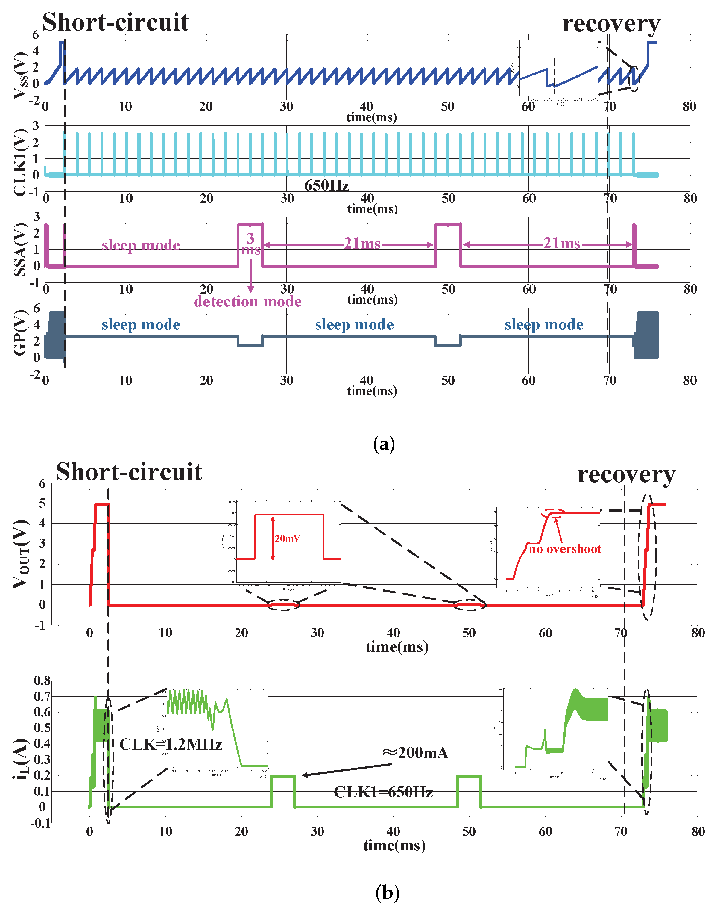
Figure 8 presents the simulation results of proposed hiccup-mode short-circuit protection technique. The results of
Figure 8a show that when short circuit occurs,
drops to 0 and repeatedly works in the form of a triangular wave, and is compared with a reference voltage to generate a clock CLK1 with a frequency of about 650 Hz. During the short-circuit period, the converter has a sleep period of about 21 ms, named sleep mode. At this time, the N and P power transistors are in the off state. After the sleep mode, there is about 3 ms to turn on the pre-charge module to detect whether the short circuit is recovered, named detection mode. When short-circuit recovery occurs in detection mode, the converter restarts directly. In particular, if the short-circuit recovery occurs during sleep mode, the converter will restart at the beginning of the detection mode.
Figure 8b presents the curve of
and inductor current
during short circuit. The working frequency of the converter is 1.2 MHz during normal operation, and the working frequency is only 650 Hz during the short-circuit period. At the same time, the inductor current is close to 0, which is only 200 mA in the detection mode, which is also far smaller than the inductor current during normal operation. Therefore, the power dissipation during the short circuit is very low. Meanwhile, when the short circuit is recovered, the converter restarts normally and there is no voltage overshoot. This is because the inductor current is very small before restarting, and there is almost no stored energy in the inductor, so there is no voltage overshoot. In fact, the restart process of the converter is similar to the process of power-on startup.
Figure 8 shows the corresponding simulation results when the short-circuit recovery occurs during sleep mode, while
Figure 9 shows the relevant simulation results when the short-circuit recovery occurs during detection mode. It can be seen from
Figure 9 that when the converter is in the detection mode, once the short circuit recovers, the circuit can be restarted immediately. The inductor current at this time charges the load through a continuous current of about 200 mA. Whenever the short circuit recovers, there is no voltage overshoot when the circuit restarts. This is because
will decrease to 0 immediately before the restart, which ensures the soft start works normally and
can always rise slowly.
Table 1 summaries the performance of the proposed boost converter. The effective power during the short-circuit period is 0, so the power consumed by the converter can be expressed as:
where
is equal to 2.5 V and
is equal to 5 V. When the converter is in detection mode,
is approximately equal to 200 mA. This is approximately equal to the inductor current, and the current consumed by the internal module is much less than 200 mA, which is almost negligible when calculating the power dissipation. The power dissipation at this time is as follows:
When the converter is in sleep mode, the converter has only a few modules that consume current,
is approximately equal to 280 uA, and the power dissipation at this time is as follows:
The time ratio between sleep mode and detection mode is 7:1, so the average power dissipation during short circuit is as follows:
It can be seen that the short-circuit power dissipation is very low.
Table 2 gives the comparison of the proposed converter with state-of-the-art converters. The inrush current of [
8] is greater than that of its normal current, while inrush current of this work is only 40% of normal current. When the converter is short-circuited, other works reduce the short-circuit current to a reasonable range. Among them, ref. [
12] reduces it to about 55% of the normal current, while this work reduces it to 40% of the normal current. This greatly reduces the short-circuit power dissipation. At the same time, the working frequency of the proposed converter during short circuit is only 0.55% of the normal frequency, which also reduces the short-circuit power dissipation.


