Article

Design of a Broadband MMIC Driver Amplifier with Enhanced Feedback and Temperature Compensation Technique

1
Communication Center, Institute of Microelectronics, Chinese Academy of Sciences, Beijing 100029, China
2
University of Chinese Academy of Sciences, Beijing 101408, China
3
Beijing Key Laboratory of New Generation Communication RF Technology, Beijing 100029, China
*
Author to whom correspondence should be addressed.
Electronics 2022, 11(3), 498; https://doi.org/10.3390/electronics11030498
Submission received: 5 January 2022 / Revised: 30 January 2022 / Accepted: 5 February 2022 / Published: 8 February 2022
(This article belongs to the Section Microelectronics)

Abstract

:
This paper presents a broadband GaN pseudo high-electron-mobility transistor (pHEMT) two-stage driver amplifier based on an enhanced feedback technique for a wideband system. Through well-designed parameter values of the feedback and the matching structure of the circuit, a relatively flat frequency response was obtained over a wide frequency band. Simultaneously, in order to reduce the fluctuation of current caused by the environmental temperature, a bias circuit with quiescent current temperature compensation was designed. The driver power amplifier, which was implemented in the form of a monolithic microwave integrated circuit (MMIC), was designed to drive a broadband high-power amplifier. The designed broadband driver amplifier for the 6 GHz to 20 GHz frequency band had a very small die size of 1.5 × 1.2 mm 2 due to the use of an optimized impedance matching structure. It exhibited a small-signal gain of 12.5 dB and output power of 26 dBm. The flatness of this driver amplifier for gain and output power was achieved as ±2.5 dB and ±1 dB over the entire frequency band, respectively. The experimental results showed up to 35 dBm in the OIP3, and the current variation range was ±5 mA after using the temperature compensation bias circuit.

1. Introduction

With the growth of wireless applications and broadband system applications, the demand for fully integrated, broadband high-power, low-cost power amplifiers is increasing, especially in modern communications, radio links, measuring equipment and military microwave systems that require a large number of radio frequency devices [1,2,3,4]. Broadband systems have better scalability in terms of potential compatibility with future wireless communication standards. With the large-scale deployment of new wireless applications, the demand for the development of high-integration and low-cost broadband MMIC power amplifier circuits from the C-band to the Ku-band is increasing, and there are already many related applications [5,6,7,8,9,10]. Many pivotal points in the design of broadband PAs need special attention. Related indicators include gain, power, flatness, input and output reflection coefficients, chip area and linearity [11]. Therefore, it is very challenging to design a broadband drive amplifier that meets actual application requirements.
Broadband MMIC amplifiers are widely used due to their small size, low cost and high reliability. Generally speaking, these chips require low return loss, good gain flatness and high broadband output power in a wideband range. In order to achieve these goals, feedback amplifiers, distributed amplifiers, lossy matched amplifiers and balanced amplifiers are widely used [11,12,13,14,15]. Feedback amplifiers establish a feedback loop between the input and output, feed back a part of the output signal to the input and realize bandwidth expansion by sacrificing part of the low-frequency gain. At the same time, they can adjust the input and output impedance. Therefore, it is easier to obtain broadband matching performance [11]. Distributed amplifiers rely on the parameters of transistors to absorb parasitic capacitance into the artificial transmission line, and ultrawideband can be realized [12,15]. Due to their structural characteristics, efficiency is particularly low. Meanwhile, the broadband characteristics of distributed amplifiers depend on more stages, and the size of distributed amplifiers is bigger. Reactive matched power amplifiers can expand bandwidth depending on the reduction of the matching Q value. They are easy to cascade, but the introduction of more resistances leads to an increase in the overall power consumption and a deterioration in noise performance [13]. Balanced amplifiers use coupling and other methods to combine two or more power amplifier signals at the input and output ports. Due to the characteristics of the coupler, the signal reflected by the port cancels out, which makes the standing wave of this structure better than other types [14]. Balanced amplifiers can achieve a wider bandwidth, but they also have disadvantages such as a huge area and a high power consumption.
In this paper, a broadband driver amplifier covering the 6–20 GHz band is designed by using an enhanced feedback structure and a series RC stable network. Using the combination of a highpass and lowpass matching network and the reasonable design of each component in the matching network, a flat frequency response is obtained. In order to reduce current fluctuations in microwave-system-level applications, a temperature compensation bias circuit is designed to realize the stability of quiescent current when the temperature changes greatly. This design adopts a 0.25 μ m GaN pHEMT process based on a SiC substrate. Compared with GaAs and CMOS, this process has the advantages of a high power density, high characteristic frequency and high breakdown voltage. This process is suitable for broadband design [16,17], which is widely used in high-power, high-voltage applications scenarios. In this paper, the performance evaluation uses a continuous wave and a two-tone signal with a tone spacing of 1 MHz. The experimental results are summarized and compared with previously reported works.

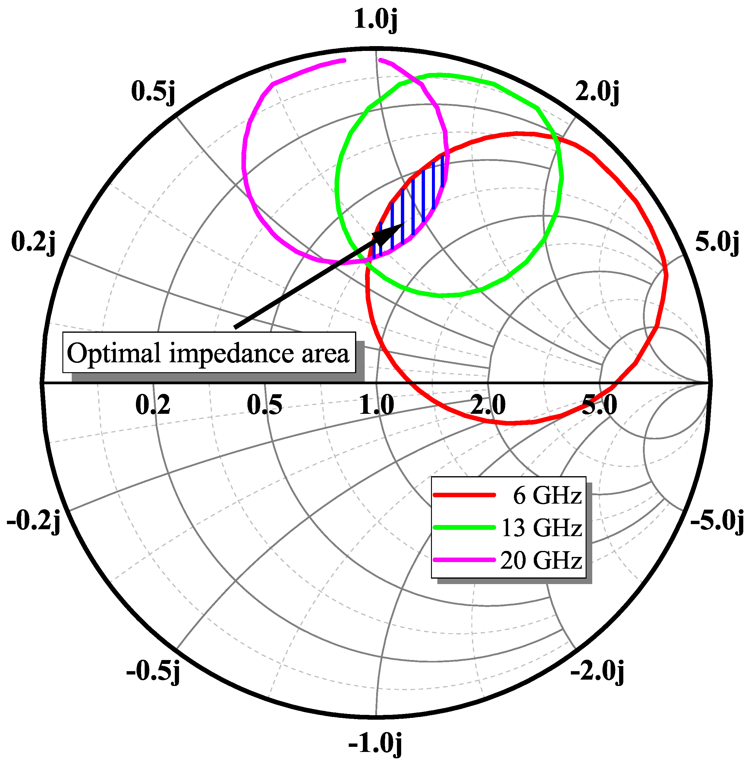
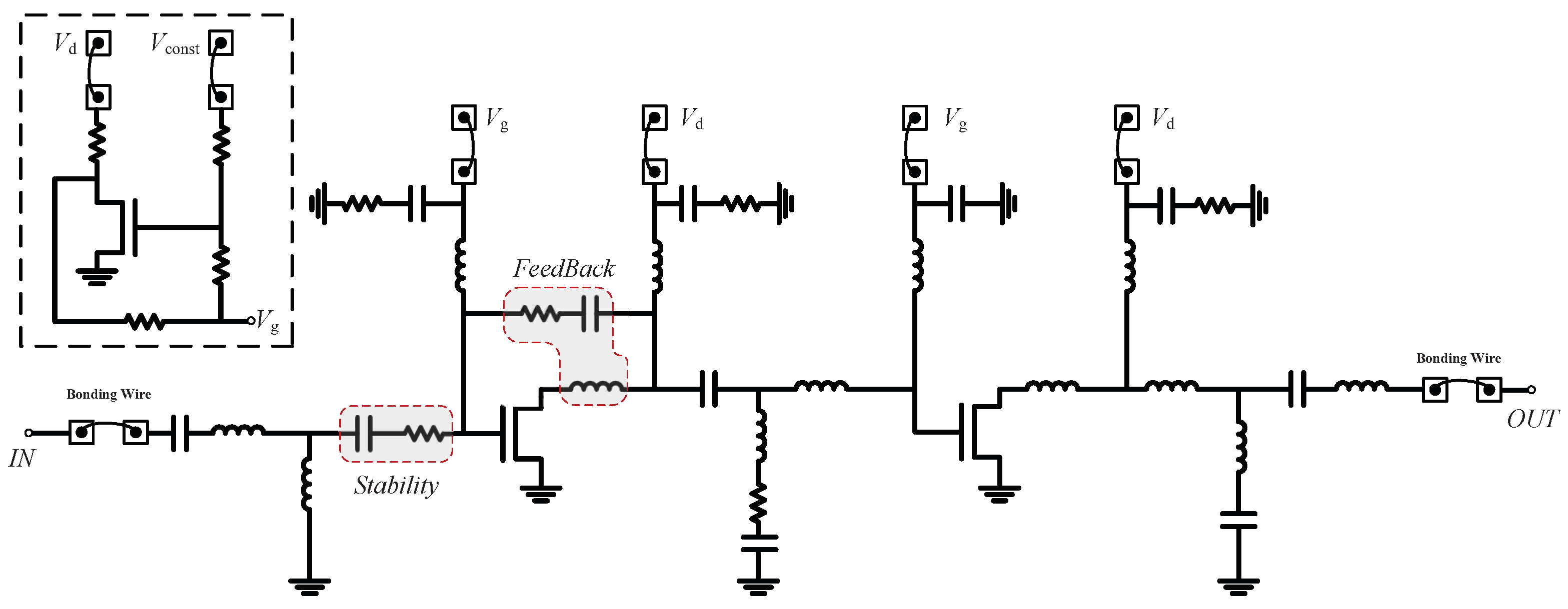
2. Broadband Driver Amplifier Design

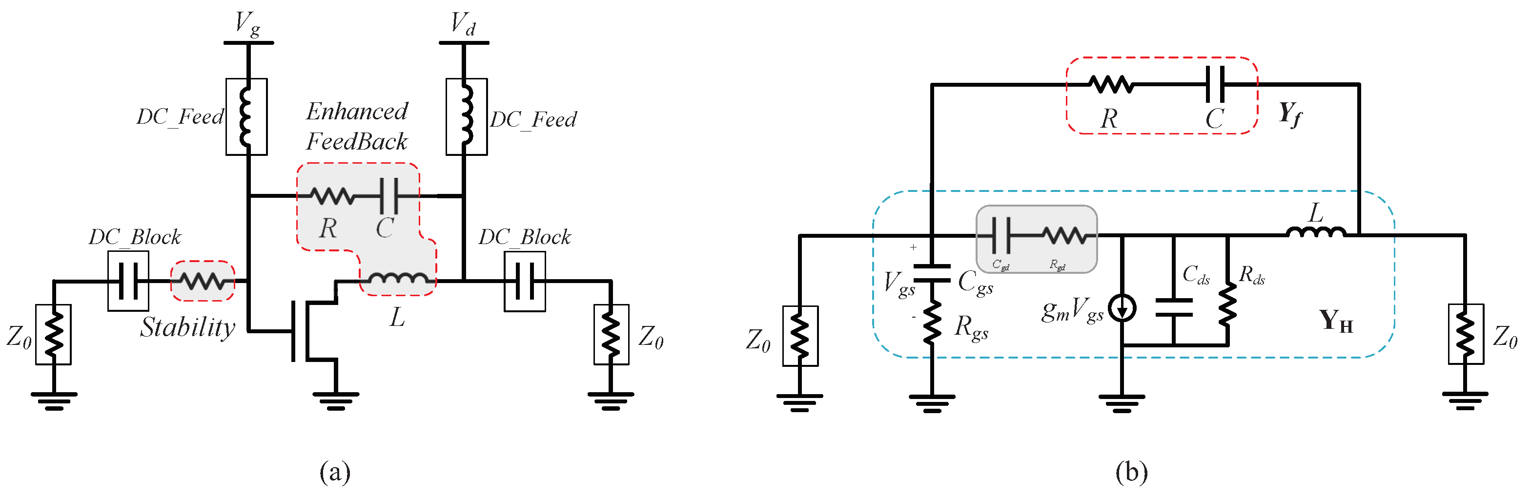
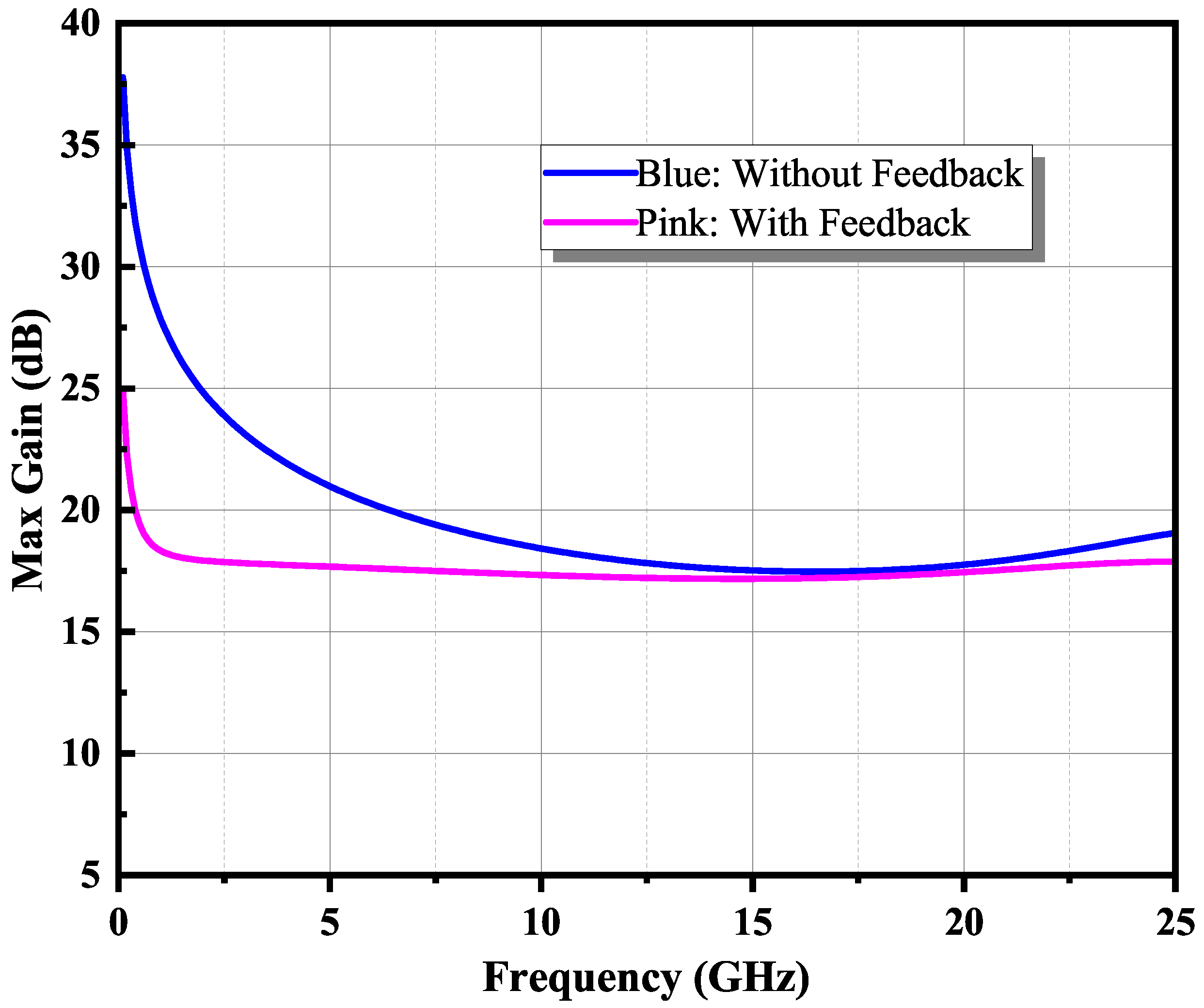
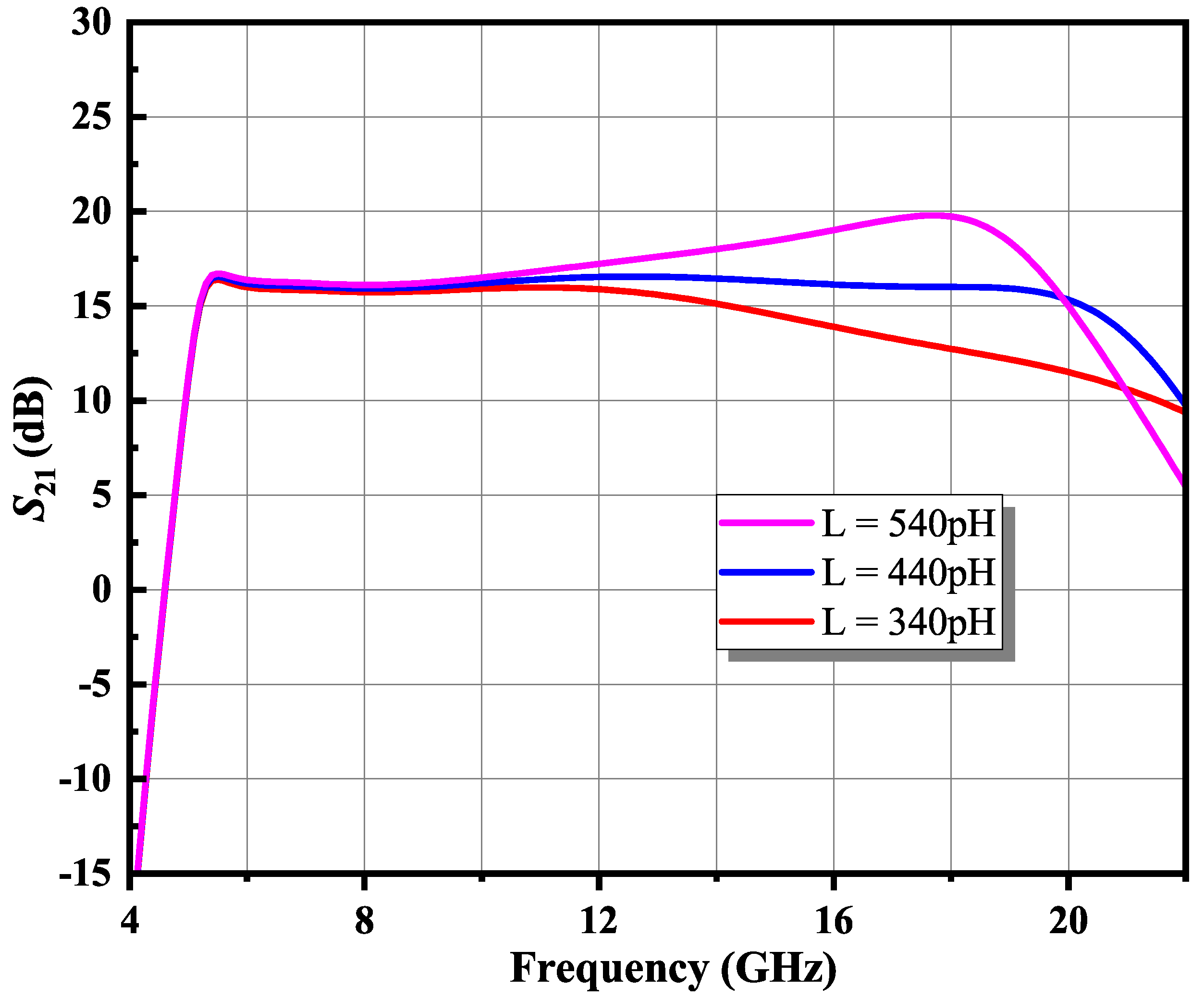
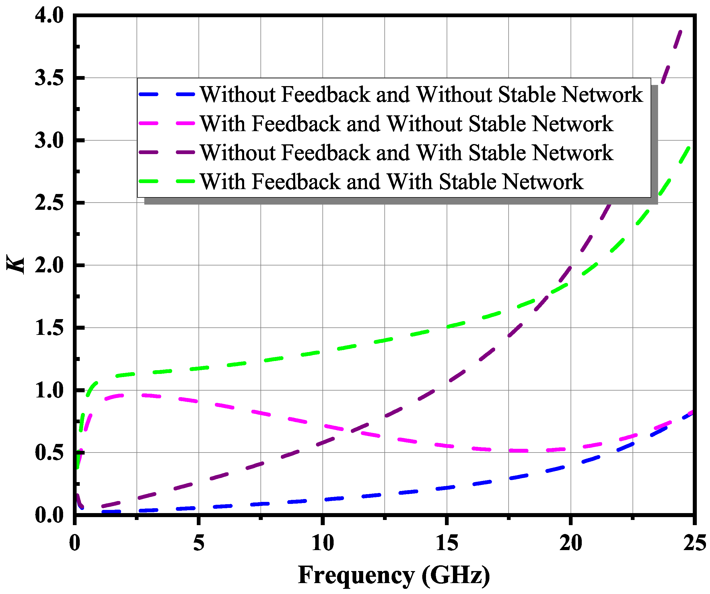
2.1. Enhanced Feedback

The driver amplifier has a two–stage cascade structure. The first stage adopts an enhanced feedback structure with a gate width of 4 × 40 μ m to achieve a flat gain in the wideband range. The second stage, which is based on output power and area requirements, has a gate width of 4 × 80 μ m, and the second stage adopts a common source structure. The choice of transistor takes into account both gain and power output, while reducing the influence of parasitic parameters [16,18]. The supply voltage for gates and drains of the two stages was −2 V and 28 V, respectively.
Advanced Design System (ADS) 2016 was utilized to simulate the performance of the driver amplifier. In order to obtain a more accurate design, all passive components were simulated using the electromagnetic (EM) simulation of ADS. The source-pull and load-pull setup of the first stage is shown in Figure 1a. In the entire frequency band, the difference between high- and low-frequency maximum stable gain (MSG) is considerable. For the purpose of achieving a good gain flatness in the broadband, an enhanced negative feedback structure was adopted. The application of the feedback circuit can obtain a flatter frequency response. Meanwhile, the feedback circuit can reduce the influence of the gain roll-off characteristics of the device itself and lower the MSG value of the low-frequency band to a certain extent [19]. A traditional feedback structure can effectively reduce the low-frequency gain, but it inevitably sacrifices part of the high-frequency performance and limits the gain bandwidth of the power amplifier. In the enhanced feedback structure adopted in this article, an RC network was connected in series between the gate and the drain, and an inductor L was connected to the drain of the transistor. The resistor was used to adjust the depth of the negative feedback and the resistance value was determined by the size and bandwidth of the gain. The capacitor C was used to isolate the DC signal to prevent the deviation of the static operating point and to adjust the phase and amplitude of the feedback signal. The inductor L was placed at the output of the transistor as a part of the feedback circuit to improve the flatness of the low-frequency gain while reducing the impact on the high-frequency gain. On one hand, considering the influence of the output capacitance of the transistor, the inductor was used to compensate the output capacitance C d s of the transistor. The inductor can reduce the amount of feedback at the high frequency and improve the matching characteristics. On the other hand, in view of the compactness of the layout, this structure removed the feedback inductance between the gate and drain. The inductance can be used as a part of the matching circuit, reducing the complexity of the entire circuit. A reasonable adjustment of the feedback components can obtain the desired gain response and stability enhancement [20]. The feedback network can shrink the distance between the center of each frequency point on the smith chart and make it easier to perform impedance matching. As shown in Figure 2, the MSG diagram with and without a feedback structure were demonstrated. The addition of a feedback structure can improve the gain flatness and system stability.
The impedance matrix of the transistor with feedback circuit can be obtained from the small-signal-equivalent model shown in Figure 1b, written as
Z H = Z 11 Z 12 Z 21 Z 22 = 1 j ω C g s + R g s 0 g m ( 1 j ω C g s + R g s ) ( R d s / / 1 j ω C d s ) j ω L + ( R d s / / 1 j ω C d s )
The output impedance Z H , O can be obtained from Equation (1):
Z H , O = j ω L + ( R d s / / 1 j ω C d s ) = j ω ( L C d s R d s 2 1 + ω 2 C d s 2 R d s 2 ) + R d s 1 + ω 2 C d s 2 R d s 2
The output resonance frequency of the transistor with feedback structure is ω and it can be expressed as:
ω = 1 C d s R d s C d s R d s 2 L 1
It can be seen from the Z matrix of Equation (1) that the addition of the feedback inductance can offset the influence of the output capacitance C d s to a certain extent. Meanwhile, the inductance reduces the Q value of the output impedance. From Equation (3), the resonance point is introduced at high frequency and the inductance value is adjusted reasonably to obtain a flat gain at high frequency.
The total admittance of transistor with the enhanced feedback circuit is written as:
[ Y ] t o l = [ Y ] H + [ Y ] f = Z 22 | Z | + y f Z 12 | Z | y f Z 21 | Z | y f Z 11 | Z | + y f
The admittance y f is given by:
y f = ( R + 1 j ω C ) 1
Thus, the overall stability factor K and small-signal gain S 21 [19,21] after adding the feedback network can be obtained, and Y 0 is the characteristic admittance.
K = 2 R e ( Y 11 ) R e ( Y 22 ) R e ( Y 12 Y 21 ) | Y 12 Y 21 |
S 21 = 2 Y 21 Y 0 Δ Y = 2 Y 21 Y 0 ( Y 11 + Y 0 ) ( Y 22 + Y 0 ) Y 12 Y 21
On one hand, the introduction of the feedback network makes the low-frequency gain response flatter as shown in Figure 2. On the other hand, as shown in Figure 3, the inductor L is connected in series with the parasitic capacitance at the output of the transistor. It can be seen from Equation (3) that increasing the value of inductance can reduce the frequency of the high-frequency resonance point. Conversely, the resonant frequency can be increased by reducing the inductance value. Thus, the bandwidth expansion and gain adjustment are realized by introducing the high-frequency resonance point. The transistor of this process has a very poor stability and has a high MSG value. So the stability network is very significant. The simulated K factor is shown in Figure 4. From the simulation data, the K factor is less than 1 in the broadband. Only adding a feedback network can not guarantee the stability of the circuit in the whole frequency band. Consequently, the designed driver amplifier adopts an RC series structure to adjust the stability. This stable network can better stabilize the circuit in this case and the K factor remains greater than 1 in a wide band after the stable network is added.
The second stage adopts a common-source structure to achieve broadband power output. An RLC network connected to the ground was adopted for the interstage matching network to minimize the impact on the output power. This RLC network can adjust stability. Simultaneously, it can participate in matching and reduce the low-frequency gain [22]. The selection of the matched impedance was determined by the optimal impedance space. The optimal impedance area was the junction area of the power contours of the high and low intermediate frequency points to ensure that the output power can meet the requirements in the broadband range, as shown in Figure 5. The power contours of Figure 5 were obtained through the simulation of ADS’s load-pull system. It was drawn by scanning the power at different frequencies. In this area, a demand output power greater than 25 dBm in the broadband was reached. The impedance point was selected at the center of the optimal impedance space to provide the maximum impedance optimization space, and the impedances thus selected are listed in Table 1.

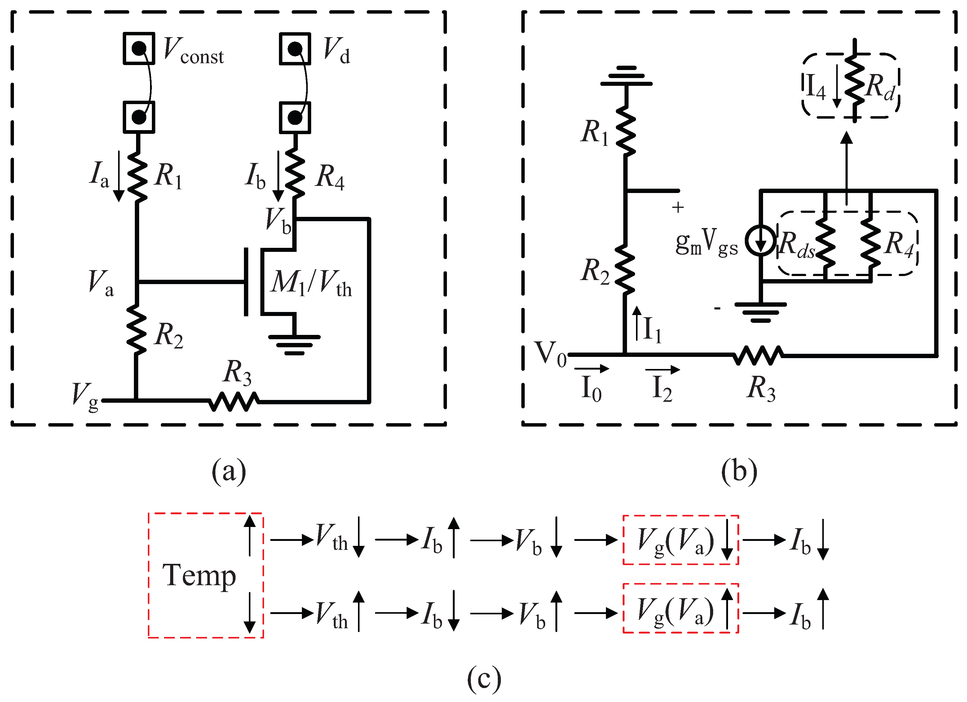
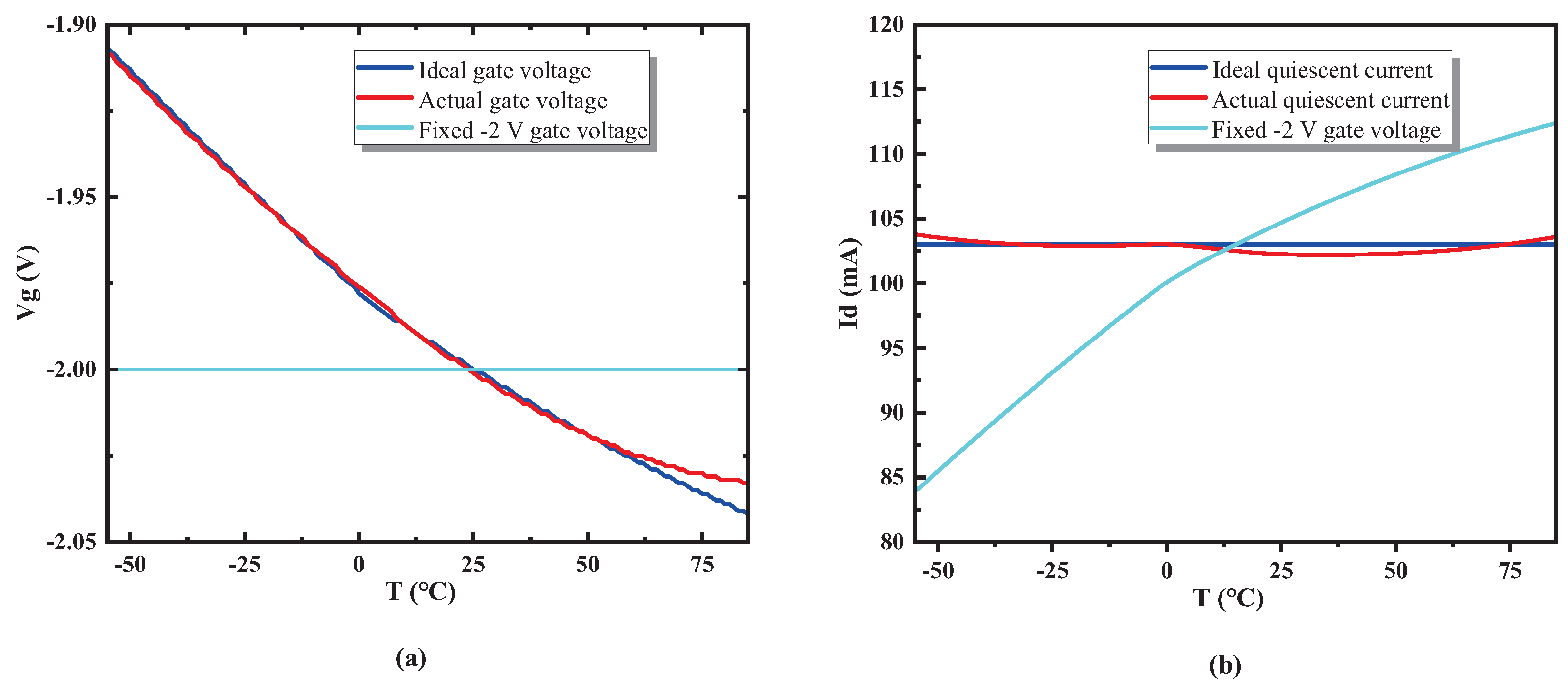
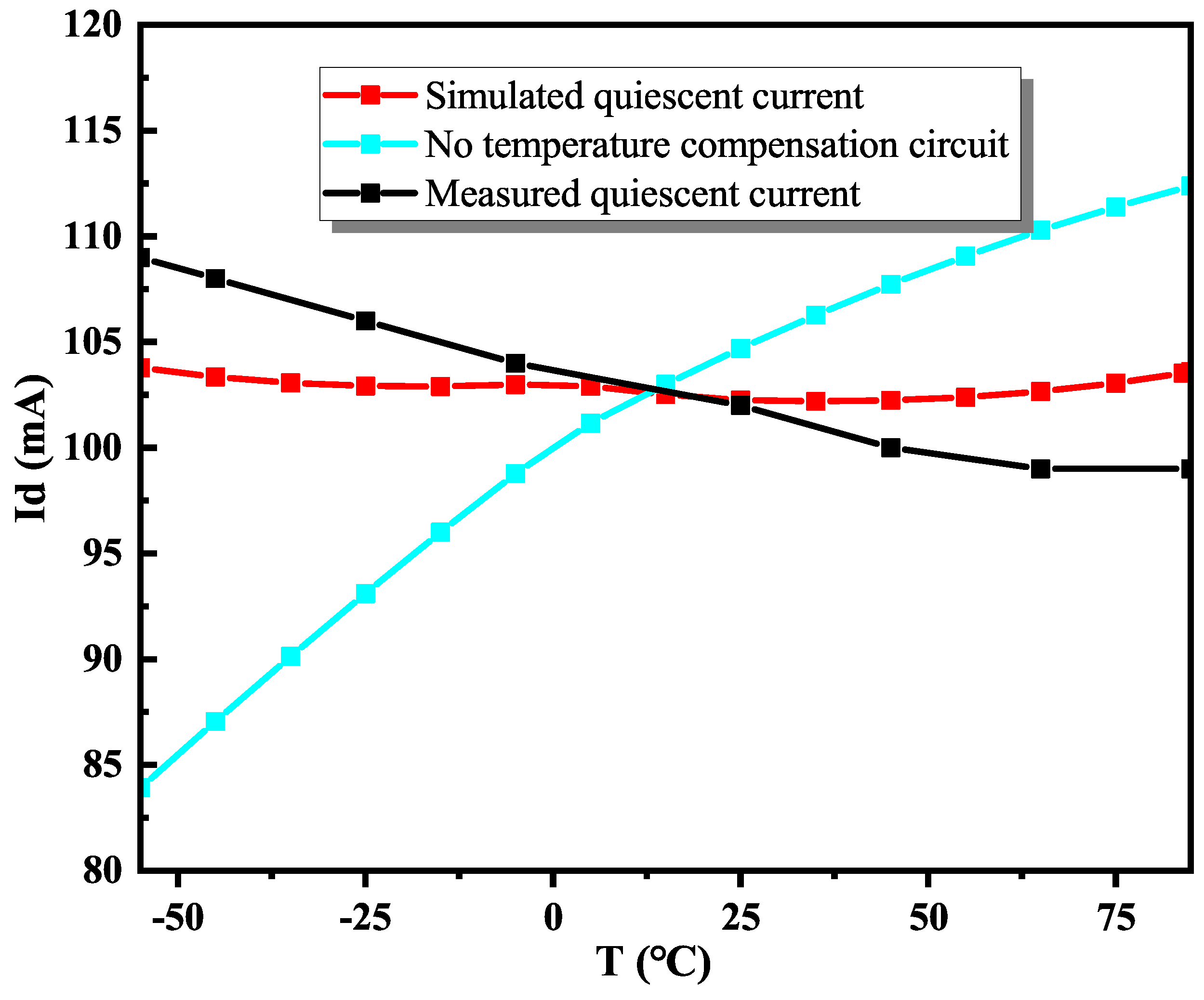
2.2. Temperature Compensation Bias Circuit

As a system-level application, a power amplifier has a significant impact on the entire system. A fluctuating current of the power amplifier affects other components. The change of ambient temperature has a significant impact on the static bias of the transistor [23,24,25,26]. With the aim of improving the influence of temperature changes on the bias state, we first analyzed the characteristics of the transistor with temperature changes under the process. Then, we designed an active temperature compensation bias circuit to improve the bias state and achieve the stability of the quiescent current.
The change in circuit performance was mainly due to the difference in transistor threshold voltage caused by temperature changes. The gate voltage was reversely compensated by a suitable circuit to offset the influence of the threshold voltage variation at different temperatures, so that the stable current state was maintained. The topological structure of the designed temperature compensation bias circuit is shown in Figure 6a. The bias circuit is composed of a transistor M1 and a corresponding voltage divider resistor. M1 is used to replicate the state of the main signal path, and the smallest size (2 × 15 μ m) in the process design kits was selected to reduce the impact on the overall circuit current. The TFR resistor was selected, which changes very little with temperature. Benefiting from the consistency of transistors manufactured on the same wafer, the threshold voltage of the bias circuit M1 had the same change as that of the transistor in the main signal path, and a negative feedback network was used to achieve a stable current control. Figure 6b shows the equivalent small-signal model of the temperature compensation bias circuit. Figure 6c shows the procedure of the voltage of each node and the branch current of the temperature compensation bias circuit with the change of temperature. It is a change process of negative feedback, and finally, the stable control of gate voltage and current on the main signal circuit is maintained.
The temperature compensation circuit must provide approximate currents at different temperatures. To achieve a relatively constant current in the power amplifier over a wide temperature range, the output voltage V 0 of the bias circuit must correspond to the variation of the temperature. As shown in Figure 7a, the blue line is an ideal gate voltage variation curve with temperature, which can realize current stability over a wide temperature range. According to the working state of the main signal circuit, the temperature compensation bias circuit needs to generate a voltage of −2 V at the central temperature, and the parameter values of the initial resistance are given by Equations (8)–(10).
g m V a = V d V b R 4 + V c o n s t V b R 1 + R 2 + R 3
V a = V c o n s t V b R 1 + R 2 + R 3 ( R 2 + R 3 ) + V b
V g = V c o n s t V b R 1 + R 2 + R 3 R 3 + V b
The temperature compensation bias circuit is regarded as a voltage source to provide the main signal circuit with a gate voltage that changes with temperature. The output impedance of the bias circuit can be obtained from the small-signal equivalent circuit shown in Figure 6b.
V g s = V 0 R 1 R 1 + R 2
I 2 = g m V g s + I 4
V 0 = I 4 R d + I 2 R 3
V 0 = I 1 ( R 1 + R 2 )
The solved output impedance R o of this temperature compensation bias circuit can be expressed as in Equation (15) from Equations (11) to (14). Compared with the traditional passive bias temperature compensation network, which adjusts the gate voltage of the transistor through the series voltage divider of the resistor [27], the output impedance of the bias network is adjusted by changing the bias state of M1 and the reasonable resistance value. By reducing the output impedance of the temperature compensation circuit, the load capacity of the circuit is increased, and the influence of the impedance change of the main circuit on the power supply is reduced.
R 0 = V 0 I 0 = ( R 1 + R 2 ) ( R 3 + R d ) ( R 1 + R 2 ) + ( R 3 + R d ) + ( g m R 1 R d )
Figure 7 shows the working state of the above-mentioned temperature compensation bias circuit under different temperatures. It can be seen that the temperature is within the range of −55 C to 85 C. As shown by the red line in Figure 7a, the bias voltage provided by the bias circuit varies within ±0.1 V. The current variation range is ±2 mA after using the temperature compensation bias circuit, and the fixed gate voltage current variation is about ±14 mA, as illustrated in Figure 7b. The temperature compensation bias circuit greatly improves the temperature characteristics of the overall circuit current and enhances the stability of the system application.

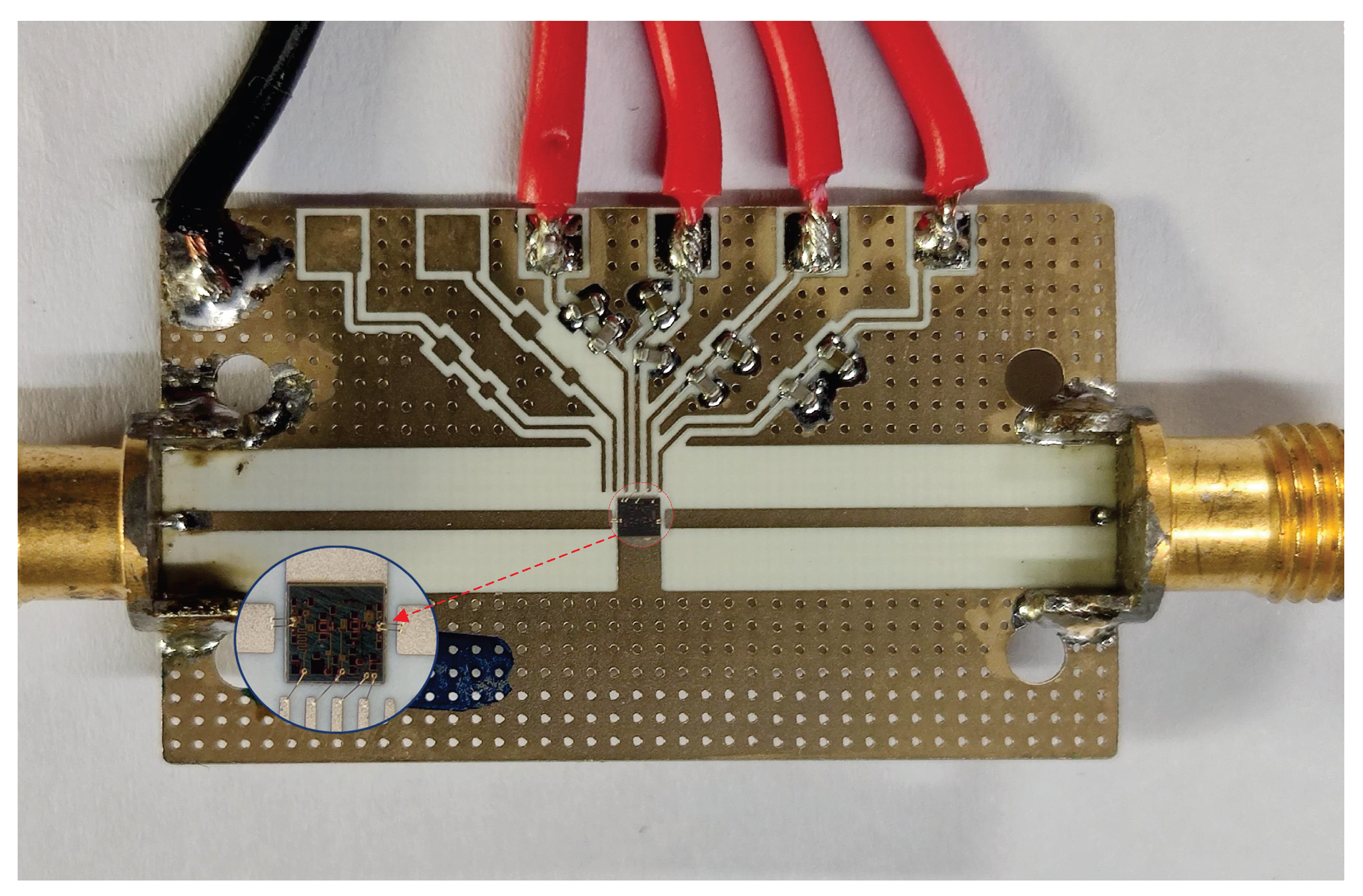
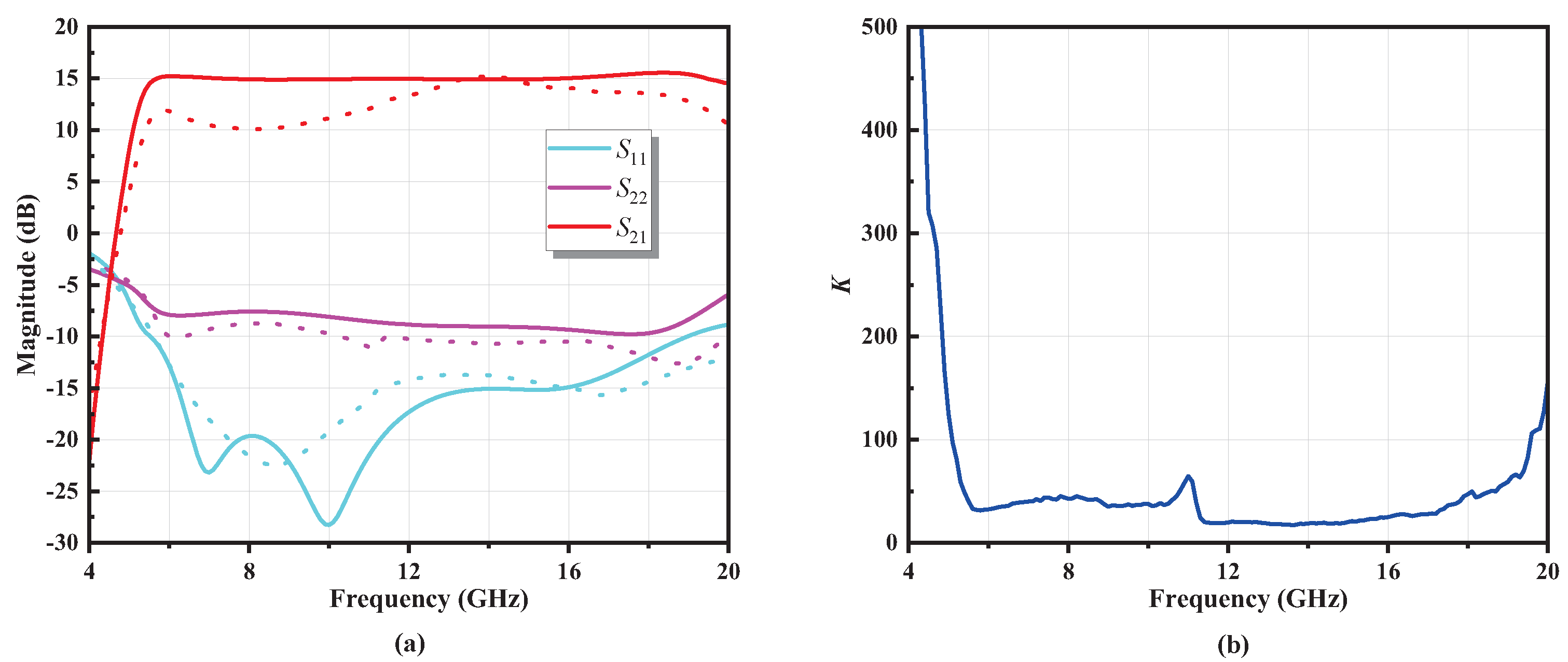
3. Experimental Results

Figure 8 shows the overall schematic diagram of the proposed broadband driver amplifier based on the enhanced feedback and temperature compensation circuits. In order to achieve better performance and simplify the matching network, a bandpass network based on the different characteristics of inductance and capacitance was adopted [28].
Figure 9 is a photograph of the proposed broadband driver amplifier chip, and the red dotted line refers to the enlarged bare die. This design adopts a 0.25 μ m GaN pHEMT process, which is very suitable for high-power and high-voltage applications because it provides a depletion transistor with a breakdown voltage of up to 120 V. By adopting an enhanced feedback structure and a simple bandpass matching form, as well as an optimized layout, the two-stage driver amplifier chip area is only 1.5 × 1.2 mm 2 . The drain supply voltage of this design is 28 V, and the quiescent current of the two stages is 33 mA and 68 mA, respectively.
Figure 10 shows the measurement results of the proposed broadband driver amplifier using a vector network analyzer on the cascaded probe station. Off-chip bypass capacitors are wire-bonded to each power supply bias pad to suppress potential self-oscillation at low frequencies. Measured S parameters which has a slight difference with the simulation results are presented in Figure 10a. In the 6 GHz–20 GHz band, the average gain is 12.5 dB with a flatness within ±2.5 dB, while the input return loss is better than −14 dB and the output return loss is lower than −8dB. For the frequency band from 6 GHz to 20 GHz, a K factor of much greater than 1 can be observed from Figure 10b. Therefore, the drive amplifier can maintain a very stable state in practical use. Figure 11a shows the large-signal measurement results that were performed at room temperature. The output power is higher than 25 dBm and the power flatness is ±1 dB. The measurement results using a two-tone signal with a tone spacing of 1 MHz are shown in Figure 11b. When the output power is 5 dBm/tone, performance of the output third-order intercept point (OIP 3 ) up to 35 dbm is obtained. Figure 12 shows the measured quiescent current of the driver amplifier, as a function of temperature. The current variation range is ±5 mA after using the temperature compensation bias circuit, and the current variation is reduced by about half compared to that without the addition of a temperature compensation circuit.
In order to obtain accurate measurement data, the loss of the measurement fixture was de-embedded during the calibration process. The difference between the simulation and measurement results can be attributed to two reasons. The first reason is that the transistor datum used in the simulation was the scaling equation extrapolation value, which was slightly different from the measured data. The second reason is that the temperature rise caused by the poor heat dissipation of the chip during the actual measurement deteriorated the performance of the chip. Due to the fabrication error, the measured quiescent current was slightly different from the simulation results, but the deviation of the quiescent current was effectively adjusted, and the slope of the quiescent current will be improved in subsequent versions.
In Table 2, the measured performance is compared to that of published broadband driver amplifier from recent years. The designed 6–20 GHz broadband driver amplifier has a smaller input reflection coefficient than other driver power amplifiers of the same type, and has a higher output power in the same frequency band, which has a wide range of applications. Compared with the distributed structure, the proposed driver amplifier has a smaller size and is suitable for miniaturized applications.

4. Conclusions

In this paper, a two–stage broadband driver amplifier was designed using a 0.25 μ m GaN process. The proposed driver amplifier works in the frequency band of 6–20 GHz. For the purpose of achieving a flat gain, the optimal transistor size was adopted. The enhanced feedback structure was used to expand the bandwidth, while improving the gain flatness and reducing the chip area. The impedance selection adopted the optimal impedance area to achieve the best broadband matching results while meeting the high power output. Meanwhile, a temperature compensation bias circuit was designed to deal with the current fluctuation in system-level applications.
The chip size of the driver amplifier was only 1.5 × 1.2 mm 2 . The fabricated driver amplifier exhibited an average gain of 12.5 dB, input reflection coefficient of smaller than −14 dB, output reflection coefficient of no larger than −8 dB. The driver amplifier exhibited a saturated output power of 26 dBm, and OIP3 figures of up to 35 dBm at 5 dBm output power in a wideband range. The fluctuation of the quiescent current with temperature was greatly reduced after adding the temperature compensation bias circuit. The discrepancies between simulations and measurements were mainly caused by the deviation in fabrication and the device model. Measurement results showed that the driver amplifier was suitable for practical broadband system applications.

Author Contributions

Conceptualization, S.Z., J.W. and X.L.; methodology, S.Z., J.W., J.Z., Z.Y. and X.L.; software, S.Z., J.W. and X.L.; validation, S.Z., J.W., J.Z. and Z.Y.; data curation, S.Z. and J.W; writing—original draft preparation, S.Z., J.Z. and Z.Y.; writing—review and editing, J.W., X.L. and Y.Y.; funding acquisition, X.L. and Y.Y.; project administration, J.W., X.L. and Y.Y. All authors have read and agreed to the published version of the manuscript.

Funding

This research was funded by Key R&D Programs in Jiangsu Province, grant number BE2018083.

Conflicts of Interest

The authors declare no conflict of interest.

References

  1. Chen, Y.F.; Quan, J.H.; Liu, Y.G.; Hu, L.L. A 6–18 GHz broadband power amplifier MMIC with excellent efficiency. J. Semicond. 2014, 35, 015007. [Google Scholar] [CrossRef]
  2. Meghdadi, M.; Medi, A. Design of 6–18-GHz High-Power Amplifier in GaAs pHEMT Technology. IEEE Trans. Microw. Theory Tech. 2017, 65, 2353–2360. [Google Scholar] [CrossRef]
  3. Oreja-Gigorro, E.; Pascual, E.D.; Sánchez-Martínez, J.J.; Gil-Heras, M.L.; Bueno-Fernández, V.; Bódalo-Marquez, A.; Grajal, J. A 6–18 GHz GaN on SiC high power amplifier MMIC for electronic warfare. In Proceedings of the 2018 13th European Microwave Integrated Circuits Conference (EuMIC), Madrid, Spain, 23-25 September 2018; pp. 85–88. [Google Scholar]
  4. Sutbas, B.; Ozipek, U.; Gurdal, A.; Ozbay, E. A 6–18 GHz GaN Power Amplifier MMIC with High Gain and High Output Power Density. In Proceedings of the 2019 European Microwave Conference in Central Europe (EuMCE), Prague, Czech Republic, 13–15 May 2019; pp. 2–5. [Google Scholar]
  5. Lee, H.; Lee, W.; Kim, T.; Helaoui, M.; Ghannouchi, F.M.; Yang, Y. 6–18 GHz GaAs pHEMT Broadband Power Amplifier Based on Dual-Frequency Selective Impedance Matching Technique. IEEE Access 2019, 7, 66275–66280. [Google Scholar] [CrossRef]
  6. Mohammadi Shirkolaei, M. A New Design Approach of Low-Noise Stable Broadband Microwave Amplifier Using Hybrid Optimization Method. IETE J. Res. 2020, 2020, 1–7. [Google Scholar] [CrossRef]
  7. Santhakumar, R.; Thibeault, B.; Higashiwaki, M.; Keller, S.; Chen, Z.; Mishra, U.K.; York, R.A. Two–Stage High–Gain High–Power Distributed Amplifier Using Dual–Gate GaN HEMTs. IEEE Trans. Microw. Theory Tech. 2011, 59, 2059–2063. [Google Scholar] [CrossRef]
  8. Kerherve, E.; Demirel, N.; Ghiotto, A.; Larie, A.; Deltimple, N.; Pham, J.M.; Mancuso, Y.; Garrec, P. A Broadband 4.5–15.5–GHz SiGe Power Amplifier With 25.5–dBm Peak Saturated Output Power and 28.7% Maximum PAE. IEEE Trans. Microw. Theory Tech. 2015, 63, 1621–1632. [Google Scholar] [CrossRef]
  9. Jeong, J.C.; Yom, I.B.; Kim, J.D.; Lee, W.Y.; Lee, C.H. A 6–18–GHz GaAs Multifunction Chip With 8–bit True Time Delay and 7-bit Amplitude Control. IEEE Trans. Microw. Theory Tech. 2018, 66, 2220–2230. [Google Scholar] [CrossRef]
  10. Lee, S.; Park, H.; Kim, J.; Kwon, Y. A 6–18 GHz GaN pHEMT power amplifier using non-foster matching. In Proceedings of the 2015 IEEE MTT-S International Microwave Symposium (IMS2015), Phoenix, AZ, USA, 17–22 May 2015; pp. 1–4. [Google Scholar]
  11. Oh, S.; Yoo, E.; Oh, H.; Koo, H.; Shin, J.; Hwang, K.C.; Lee, K.Y.; Yang, Y. Frequency Selective Degeneration for 6–18 GHz GaAs pHEMT Broadband Power Amplifier Integrated Circuit. Electronics 2020, 9, 1588. [Google Scholar] [CrossRef]
  12. Chang, H.Y.; Liu, Y.C.; Weng, S.H.; Lin, C.H.; Yeh, Y.L.; Wang, Y.C. An Ultra–wideband GaAs pHEMT Distributed Power Amplifier. In Proceedings of the 2019 IEEE 4th Advanced Information Technology, Electronic and Automation Control Conference (IAEAC), Chengdu, China, 20–22 December 2019; pp. 2144–2147. [Google Scholar]
  13. Lin, Q.; Wu, H.F.; Hua, Y.N.; Chen, Y.J.; Hu, L.L.; Liu, L.S.; Chen, S.J. A 2–20-GHz 10–W High–Efficiency GaN Power Amplifier Using Reactive Matching Technique. IEEE Trans. Microw. Theory Tech. 2020, 68, 3148–3158. [Google Scholar] [CrossRef]
  14. Pang, J.Z.; Chu, C.H.; Li, Y.; Zhu, A. Broadband RF–Input Continuous Mode Load Modulated Balanced Power Amplifier With Input Phase Adjustment. IEEE Trans. Microw. Theory Tech. 2020, 68, 4466–4478. [Google Scholar] [CrossRef]
  15. Shin, D. H; Yom, I.B.; Kim, D.W. 6--GHz--to--18--GHz AlGaN/GaN Cascaded Nonuniform Distributed Power Amplifier MMIC Using Load Modulation of Increased Series Gate Capacitance. ETRI J. 2017, 39, 737–745. [Google Scholar] [CrossRef]
  16. Hamza, K.H.; Nirmal, D. A review of GaN HEMT broadband power amplifiers. AEU-Int. J. Electron. Commun. 2020, 116, 153040. [Google Scholar] [CrossRef]
  17. Florian, C.; Traverso, P.T.; Santarelli, A. A Ka-Band MMIC LNA in GaN-on-Si 100-nm Technology for High Dynamic Range Radar Receivers. IEEE Microw. Wirel. Compon. Lett. 2021, 31, 161–164. [Google Scholar] [CrossRef]
  18. Marsh, S.P. MMIC power splitting and combining techniques. Des. Rfics Mmics 1997, 391, 1–6. [Google Scholar]
  19. Peng, L.; Chen, J.; Zhang, Z.; Huang, Y.; Wang, T.; Zhang, G. Design of broadband high-gain GaN MMIC power amplifier based on reactive/resistive matching and feedback technique. IEICE Electron. Express 2021, 18, 20210313. [Google Scholar] [CrossRef]
  20. Kim, K.; Seo, M.; Jeon, J.; Kim, M.; Kim, H.; Lim, H.; Park, C.; Yang, Y. Design of a broadband power amplifier using an optimized feedback network. Microw. Opt. Technol. Lett. 2011, 53, 2846–2851. [Google Scholar] [CrossRef]
  21. Pozar, D.M. Microwave Engineering, 4nd ed.; John Wiley & Sons: Hoboken, NJ, USA, 2011; pp. 154–196. [Google Scholar]
  22. Bahl, I. Fundamentals of RF and Microwave Transistor Amplifiers; John Wiley & Sons: Hoboken, NJ, USA, 2009; pp. 479–490. [Google Scholar]
  23. Zhang, J.; Liu, T.J.; Ye, Y.; Peng, Y.; Zhang, Y.; Lin, H. Automatic temperature compensation software for RF power amplifiers. In Proceedings of the 2011 International Conference on Electronics, Communications and Control (ICECC), Ningbo, China, 9–11 September 2011; pp. 1909–1912. [Google Scholar]
  24. Li, W.T.; Wang, S.M.; Lin, G.C. A WLAN RF CMOS power amplifier with power detector, high harmonic suppression, and temperature compensation. In Proceedings of the 2015 European Microwave Conference (EuMC), Paris, France, 7–10 September 2015; pp. 436–439. [Google Scholar]
  25. Chen, C.; Xu, X.; Yang, X.; Sugiura, T.; Yoshimasu, T. A 20–30 GHz high efficiency power amplifier IC with an adaptive bias circuit in 130-nm SiGe BiCMOS. In Proceedings of the 2017 IEEE 17th Topical Meeting on Silicon Monolithic Integrated Circuits in RF Systems, Phoenix, AZ, USA, 15–18 January 2017; pp. 88–90. [Google Scholar]
  26. Gaddour, A.; Dghais, W.; Hamdi, B.; Ben Ali, M. Temperature Compensation Circuit for ISFET Sensor. J. Low Power Electron. Appl. 2020, 10, 2. [Google Scholar] [CrossRef] [Green Version]
  27. Tian, Y.; Wang, G.; Yang, J.; Tong, W.; Cao, Y.; Chen, Y.J.; Yang, G.; Song, Y.X. A Ka–band TDD front–end chip with 24.7% bandwidth and temperature compensation technology. IEICE Electron. Express 2017, 14, 20170350. [Google Scholar] [CrossRef] [Green Version]
  28. Bowick, C. RF Circuit Design; Elsevier: Amsterdam, The Netherlands, 2011; pp. 447–468. [Google Scholar]
Figure 1. (a) The source and load-pull setup of the proposed structure. (b) Equivalent circuit model of the proposed structure.
Electronics 11 00498 g001
Figure 2. Simulated maximum gain of the first stage with and without enhanced feedback structure.
Electronics 11 00498 g002
Figure 3. Simulation of the dependence of the S 21 for different feedback inductance values.
Electronics 11 00498 g003
Figure 4. Simulated stability factor K with and without the insertion of feedback and stable networks.
Electronics 11 00498 g004
Figure 5. Optimal impedance area in power contours of different frequency.
Electronics 11 00498 g005
Figure 6. (a) Schematic of the temperature compensation bias circuit. (b) Equivalent small-signal model of the temperature compensation bias circuit. (c) Current and voltage change direction with temperature.
Electronics 11 00498 g006
Figure 7. Simulation results of the temperature compensation bias circuit. (a) Temperature compensation circuit output voltage. (b) Quiescent current of the drive amplifier.
Electronics 11 00498 g007
Figure 8. Complete schematic diagram of the designed broadband driver amplifier.
Electronics 11 00498 g008
Figure 9. Photograph of the implemented broadband driver amplifier.
Electronics 11 00498 g009
Figure 10. Experimental results of the proposed driver amplifier. (a) Comparison between simulated (solid line) and measured (dash line) small-signal performance. (b) Measured stability factor of the driver amplifier.
Electronics 11 00498 g010
Figure 11. Experimental results of the proposed driver amplifier. (a) Comparison between simulated and measured large-signal results. (b) OIP3.
Electronics 11 00498 g011
Figure 12. Comparison between simulated and measured quiescent current.
Electronics 11 00498 g012
Table 1. Optimal impedance values for the first and second stage of the transistors.
StageFirst StageSecond Stage
Size ( μ m)4 × 404 × 80
Z L , o p t ( Ω )38 + j*4235 + j*29
Z S , o p t ( Ω )18 + j*2510 + j*12
Table 2. Comparison with previously published broadband amplifiers.
ReferenceProcessStructureFreq (GHz)BW (%)Gain (dB)IRL (dB)ORL (dB)Pout (dBm)Size (mm 2 )
[5]0.15 μ m GaAsTwo-stage6–1810017.4<−8N/A19.21.2 × 0.82
[7]0.2 μ m GaNDistributed2–1816019.5<−14<−5264 × 2
[9]0.25 μ m GaAsTwo-stage6–1810012<−10<−9155 × 2
[19]0.1 μ m GaNTwo-stage22–2720.124<−9<−10301.8 × 0.87
This work0.25 μ m GaNTwo-stage6–2010812.5<−14<−8261.5 × 1.2
Publisher’s Note: MDPI stays neutral with regard to jurisdictional claims in published maps and institutional affiliations.

