1. Introduction
As decarbonization requires a higher share of electric power, the importance of power electronics also increases. Most power electronics use switching transistors, and the application of new types of transistors such as silicon-carbide (SiC) and gallium-nitride has led, due to the possibility of much faster switching and, consequently, less heat dissipation, to a significant volume reduction in power electronic systems. However, fast switching comes at the cost of higher electromagnetic emissions: a factor of 10 faster rise time results in 20 dB more emissions at large frequencies [
1].
To avoid expensive redesigns when emission requirements are not met, computer simulation has become an indispensable tool in designing and optimizing the electronic and electromagnetic properties of power electronics. Often, circuit simulations are used, which are augmented by parasitic elements to include electromagnetic properties of the electromechanical setup of the test system.
Rondon-Pinilla et al. [
2] used this approach to model a buck converter with an SiC junction-gate field-effect transistor (JFET). To predict its conducted emissions up to 30 MHz, they propose to model the parasitics by means of impedance-measurement-based circuit models, whereas a behavioral model based on known physical properties was used to model the transistor. Conducting time domain simulations, the authors achieved deviations between measurement and simulation below 5 dB up to 10 MHz and up to 10 dB between 10 MHz and 30 MHz.
In [
3], Ishii et al. propose a similar strategy to model the parasitics, but they used a measurement-based behavioral model for their transistors. Similar deviations are observed up to 10 MHz, whereas higher deviations, as in [
2], are reported for frequencies between 10 MHz and 30 MHz.
In contrast to the two previously summarized papers, Chen et al. [
4] propose developing circuit model descriptions for the paracitics of a switched-mode power supply by means of 3D full-wave finite element (FE) simulations. However, they restrict their FE simulations to the description of the mutual coupling of specific components. It turns out that for frequencies up to 10 MHz, good agreement between simulation and measurement is observed. For higher frequencies, deficiencies in their models are given.
Schröder et al. [
5] investigate the switching behavior of a power module in a double-pulse setup. They compare the impact of three different FE simulation-based models: two models developed at fixed frequencies (10 Hz and 1 MHz) and a broadband macro-model based on vector fitting (VF) [
6]. A significant impact from the model types is reported. The parasitics model obtained from the 10Hz simulation in particular is not able to predict prominent effects such as skin effects. Furthermore, it is reported that for frequencies higher than 100 MHz, the used transistor models are insufficient.
Zhang et al. [
7] report the radiated electromagnetic interference of a 7.2 W dual active bridge DC–DC converter. The circuit model, which is used to prescribe the emissions, is developed by means of measurements of the entire setup in an anechoic chamber. The switching device is characterized by measurements, too. Up to frequencies of 500 MHz, this solely measurement-based model of a DC–DC converter is able to predict the radiated emissions with a 5 dB deviation from the measurement.
A similar approach is used in [
8] to predict the radiated emissions of an automotive converter up to 500 MHz. In addition to the measurement-based models of cabling, etc., an FE simulation-based model of the converter’s PCB is incorporated in the model-based EMI prediction. The main advantage of this approach is that the impact of changes in the layout can easily be investigated. Nevertheless, coupling effects between components on the PCB are not taken into account.
The RF interference in mobile platforms caused by switched-mode power supplies is addressed in [
9,
10]. Here, current paths that enable the transistor to create noise are identified and modeled using HSPICE circuit descriptions. The transistor is also modeled in HSPICE, which requires corresponding libraries.
In [
11], the radiated emissions analysis of switching regulators used in laptops is performed on the basis of simulation only. The PCB is modeled using the 3D solver of the CST Studio Suite
® [
12]. This software uses vector fitting to obtain a circuit representation of the computed structure, which is then solved in a transient simulation. With the known currents and voltages at the circuit ports, the radiated fields around the 3D structure can be computed. The authors use a SPICE model of the switches and investigate resonances in the radiated fields up to 1 GHz.
The same approach is chosen in [
13], where Ansys tools [
14] are used for a power module with wide band-gap SiC MOSFETs of 1200 V/36 A. A behavioral model of the transistors is created based on data-sheet information. This model is used in a circuit simulation, which is complemented by circuit parasitics obtained from a 3D electromagnetic solver, and a comparison to measurements is made up to 100 MHz. It is reported that the frequencies of the spectral peaks are approximately matched, but the amplitude differs by several orders of magnitude.
Whereas modeling electromagnetic emissions in the range of up to 100 MHz is well-established, we conclude that above 100 MHz, many different approaches exist. Lots of effort is spent on the examination of the impact of the 3D geometry and on modeling the transistor as noise source. References to the measurement of the device under test are needed to verify assumptions and calibrate the computer model.
In this paper, we develop a universally valid approach to simulate the conducted electromagnetic interference (EMI) of power systems. According to the standard CISPR25 [
15], conducted emission measurements are performed up to a frequency of 108 MHz to cover the FM radio range. However, comparably new services are found at higher frequencies (e.g., Digital Audio Broadcasting (DAB) is performed between 170 MHz and 230 MHz), and conducted measurements are often performed far beyond 108 MHz to obtain an estimate of the emission. For this reason, our model aims to extend the very high-frequency (VHF) band which ends at 300 MHz [
16].
We particularly pick up on the description of the impact of the 3D geometry and on transistor models. As a demonstration, we use a four-layer printed circuit board (PCB) with a halfbridge composed of two gallium-nitride (GaN) semiconductors, which drive a resistive–inductive load. We show that the PCB can be completely modeled in a 3D simulator without any further, time-consuming simplifications. Additionally, we propose a simple model that accurately describes the GaN semiconductor based on datasheet information and the measurement of the switching event. More precisely, we answer the following questions:
Which parts of the system are best characterized by solving Maxwell’s Equations, and which method must be to solve them?
Which parts of the system must be characterized by measurement?
What is needed to efficiently generate a transistor model, and what are its accuracy limits?
With which method are all the above-mentioned components combined into a system simulation that predicts emissions?
Answering these questions, we establish a 10-point procedure using the CST Studio Suite that allows us to conveniently set up robust simulation models for many types of power electronic systems. We validate our model by measurements up to a frequency of 400 MHz.
3. Modeling
In this section, the development of a numerical 3D model of the DUT and the measurement setup presented above is discussed. These models can be utilized to predict the conducted EMC behavior from 9 kHz up to 400 MHz.
3.1. Three-Dimensional EM Model of PCB and Measurement Setup
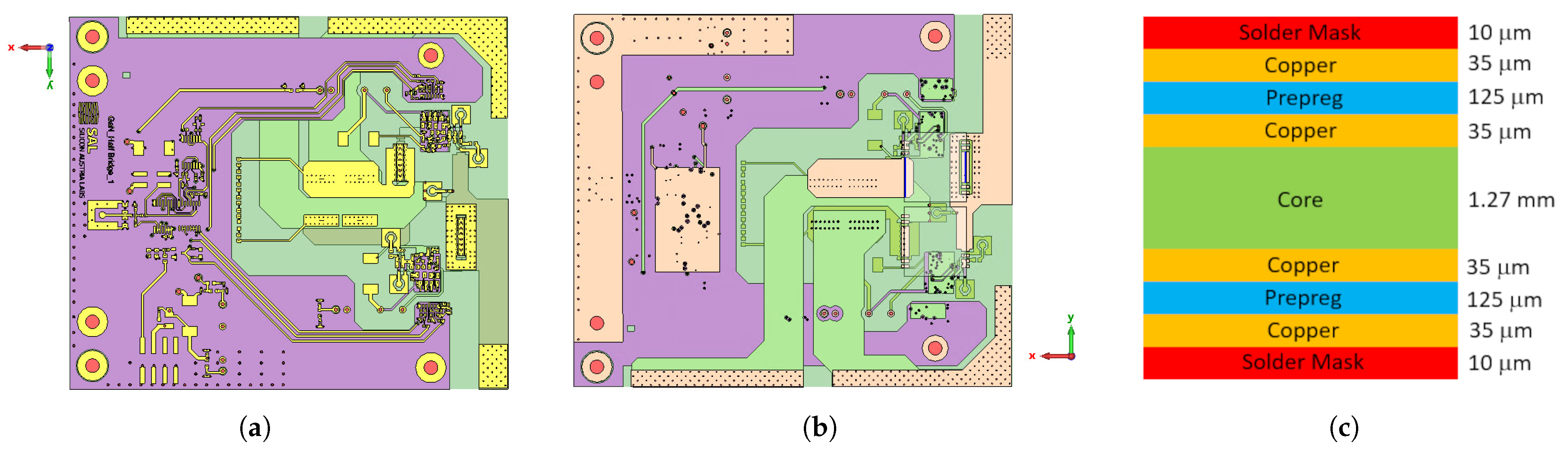
First, a 3D model of the PCB is generated by importing the respective ODB++ data files into the CST Studio Suite. The result is depicted in
Figure 7a,b. The board comprises four conductive copper layers, a substrate core material, and two prepreg insulation layers (see
Figure 7c). The PCB material parameters are summarized in
Table 1, where the values for the relative permittivity of the substrate core material, the dielectric prepreg, and the solder mask are manufacturer recommendations.
The conducting layers are modeled by using a surface impedance material model available in the CST Studio Suite [
20]. This model significantly reduces the computational effort because it only requires numerical solutions on the conductor surface. Hence, there is no discretization of the region needed within the conductor. However, this surface impedance model is only accurate if the skin depth within the conductor is smaller than its thickness. Therefore, one must estimate the model inaccuracies exhibited by this simplified material model where the skin depth exceeds the conductor’s thickness. For our simulations, we considered that copper exhibits a conductivity
=
and a relative permittivity
= 1; hence, one can calculate the lower frequency limit of the surface impedance model as follows:
where
d is the conductor thickness. By substituting the values from
Figure 7c and
Table 1 for
d,
, and
, one obtains a lower frequency limit of
= 14.26 MHz; hence, the conductor losses are not estimated properly up to 14.26 MHz by the surface impedance model. However, these losses were investigated by means of numerical simulations, and they do not exceed 10 m
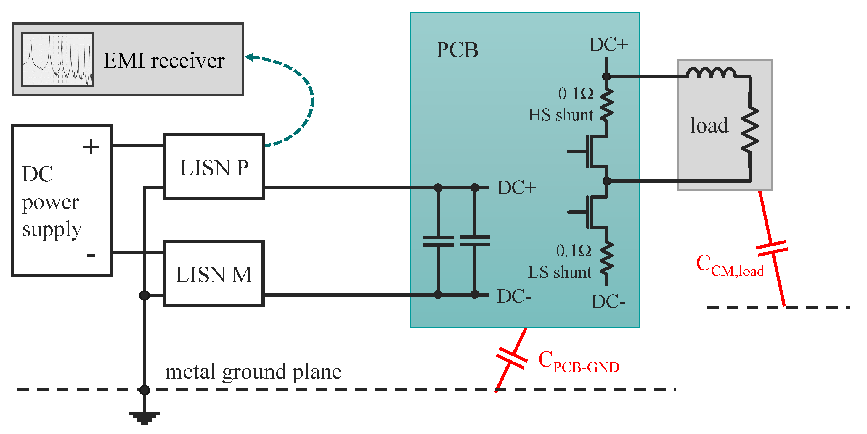
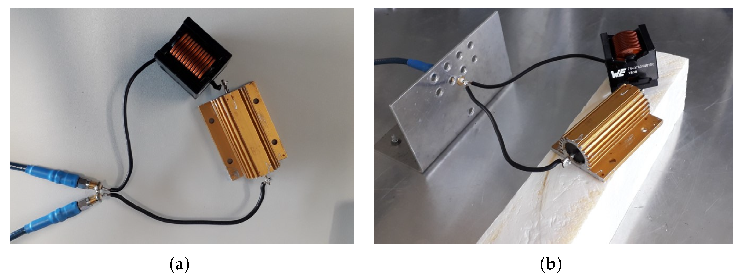
. Therefore, they are presumed negligible compared to the losses caused by the external shunt resistors mounted on the PCB (see
Figure 2).
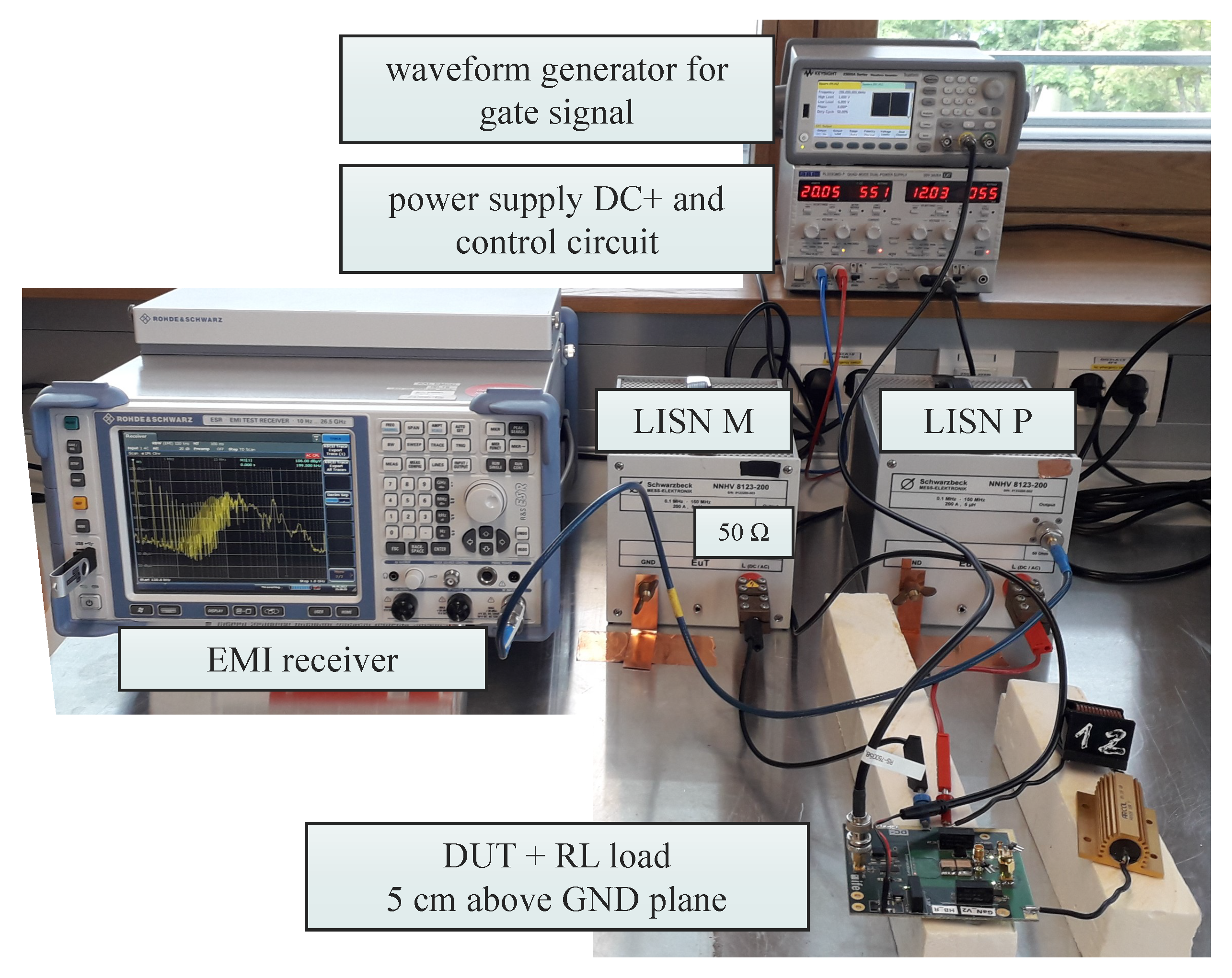
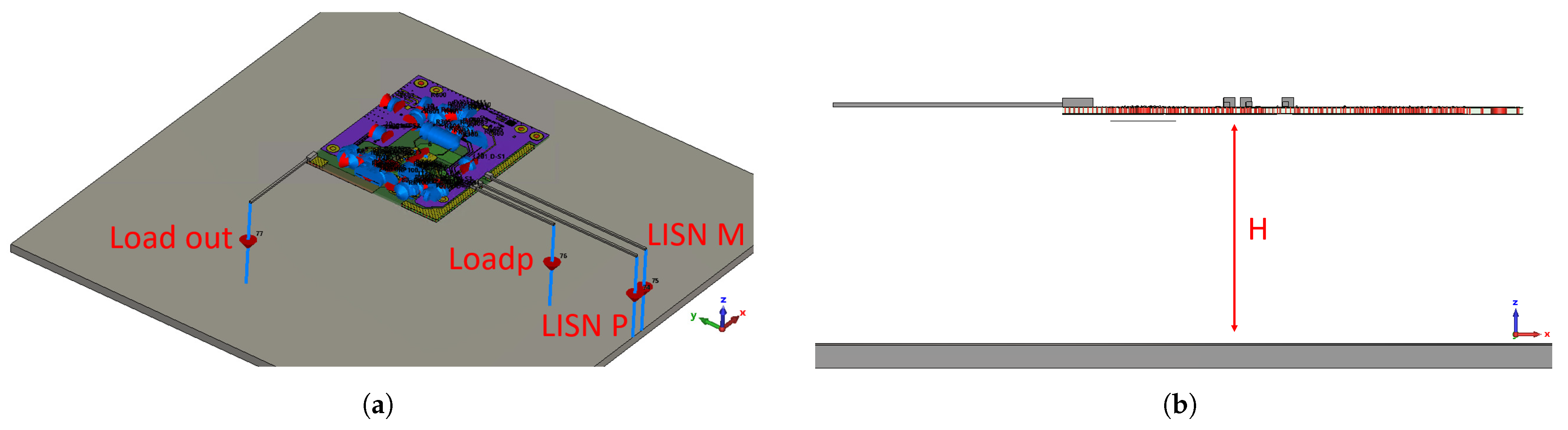
To obtain simulation results that are comparable to CISPR25 [
15] measurements, one has to model not only the investigated PCB but also the test bench setup, including the metal reference table and supply cables connected to the LISN networks (see
Figure 8a, LISN M/P) and the load (see
Figure 8a, Load out/p), respectively. This work considers a test setup, where the PCB is placed 50mm above a metal table, as shown in
Figure 5.
3.2. Component Modeling
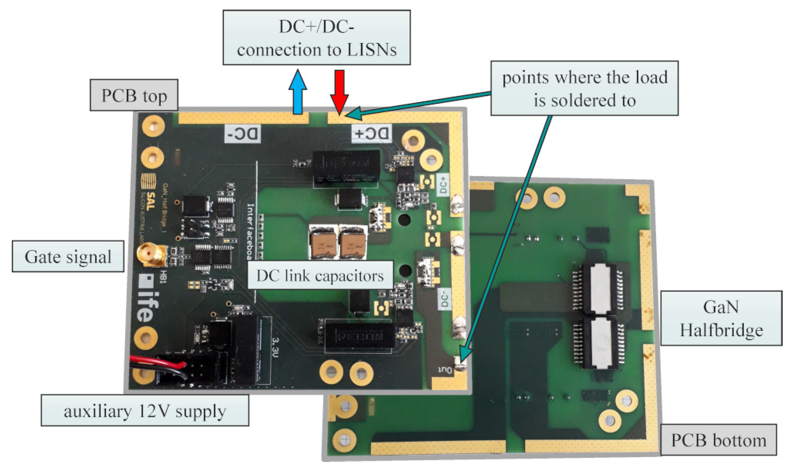
To fully characterize the behavior of a PCB, one must also consider the electromagnetic behavior of external components which are mounted on the PCB to operate the circuit. The investigated test PCB has in total 176 mounted components (see
Figure 1) which may influence the conducted EMC’s behavior. One may investigate the influence of all single components on the overall EMC behavior, but this approach is computationally very expensive; therefore, it is not feasible. The presented approach categorizes the components into two groups. The components which are not part of the halfbridge circuit shown in
Figure 2 comprise the first group. These components do not experience fast-switching, high-load currents; therefore, it is presumed in a first approximation that their impact on the conducted emissions due to parasitic and non-linear effects is negligible for the frequency range of interest.
The components which are part of the halfbridge circuit (see
Figure 2) comprise the second group, and they are considered critical since they experience fast switching load currents; hence, their impact on the conducted EMC behavior is investigated very carefully. An exception are the shunt resistors present in the halfbridge circuit since the manufacturer ensures a tolerance of 1% and a high reliability [
21]. Therefore, these resistors are included in the first component group.
The two component groups are treated differently in the 3D model. The electromagnetic behavior of the first component group is considered directly in the 3D FEM simulation in terms of impedance boundary conditions (face lumped elements). Therefore, component variations are not considered in the simulations. The electromagnetic behavior of the critical components is not directly considered in the 3D FEM simulation. Instead, an interface to a SPICE simulation framework is defined (face lumped port) for each of these components where arbitrary external circuit elements can be attached. The two modeling approaches for the components are discussed in detail in
Section 3.2.1 and
Section 3.2.2.
3.2.1. Face Lumped Elements
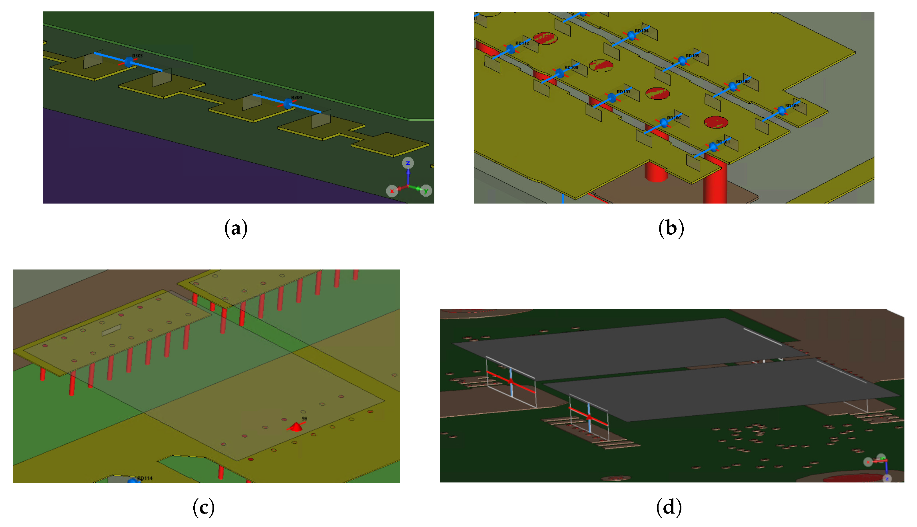
All components that are part of the first component group are treated as ideal components; hence, they are modeled as face lumped elements with ideal electrical behavior, as depicted in
Figure 9a,b. With this modeling approach, one can consider the electrical R, L, and C behaviors of the corresponding component within the 3D simulation using surface impedance boundary conditions. Although the simulated parasitic self-inductance of these lumped element models, as well as their mutual inductive coupling, exhibits certain inaccuracies. they are still feasible to approximate parasitic inductive effects, as discussed in [
22]. The significant advantage of these models is their simplicity in terms of computational effort and that they can be generated automatically from the imported odb++ database in the CST Studio Suite. Therefore, a large number of external components can be considered with very low modeling and computational effort.
3.2.2. Face Lumped Ports
The components that are part of the second component group are of special interest since it is presumed that they dominate the conducted EMC characteristics up to 400 MHz due to fast switching load currents through the devices. To verify this presumption, we modeled these components with face lumped ports (see
Figure 9c,d) to investigate their impact on the overall conducted EMC characteristics. These face lumped ports enable an interface between 3D FEM simulation and SPICE simulation; hence, arbitrary circuit models of the components can be attached to identify the source of conducted emission peaks. The CST Studio Suite provides a feature that allows the automatic generation of such face lumped ports from the imported odb++ database. The generation of face lumped ports is very similar to the generation of face lumped elements, and hence their modeling effort is also low. However, the number of ports significantly influences the computational effort since each port must be excited by the electromagnetic solver to determine its reflection and transmission behavior. Therefore, one should keep the number of ports as small as possible to facilitate a computationally efficient 3D simulation.
3.3. EM Solver and Computational Effort
The 3D numerical simulations were performed in the CST Studio Suite using the finite element method (FEM) in the frequency domain with tetrahedral mesh cells. In the frequency domain, the Maxwell’s equations are [
23]:
where
and
are the electric and magnetic field strengths, respectively;
is the angular frequency;
is the total current density comprising conduction current density
and source current density
;
and
are the electric and magnetic flux density, respectively; and
is the electric charge density. The constitutive equations are as follows [
23]:
where
and
are the permeability and permittivity of free space, respectively;
is the relative permeability;
is the relative permittivity; and
is the conductivity.
Combining Equations (
2) and (
3) with the constitutive equations lead to the wave equation for the electric field intensity
:
that is solved in its weak form by the FEM Solver provided in CST. The 3D model is discretized by using a hp adaptive mesh refinement [
24] for tetrahedral elements. The adaptive mesh procedure calculates an estimation error of the field solution and improves the mesh quality where the estimation error is high until a convergence criterion is reached [
12]. A convergence criterion of 0.04 was recommended by the CST support. The equation system was solved by a direct solver, and a broadband convergence criterion was satisfied after calculating 13 frequency samples.
Table 2 summarizes the computational effort for mesh generation and for solving the equation system. As shown, the 3D simulations are computationally comparably expensive; hence, it is not feasible to consider the impact of component variations directly in the 3D simulation model. However, the expensive 3D simulation needs to be run only once, and hence this approach is also valid for electronic-based systems which are more complex than the one investigated in this paper since a computation time of several hours up to one night does not slow down product development time.
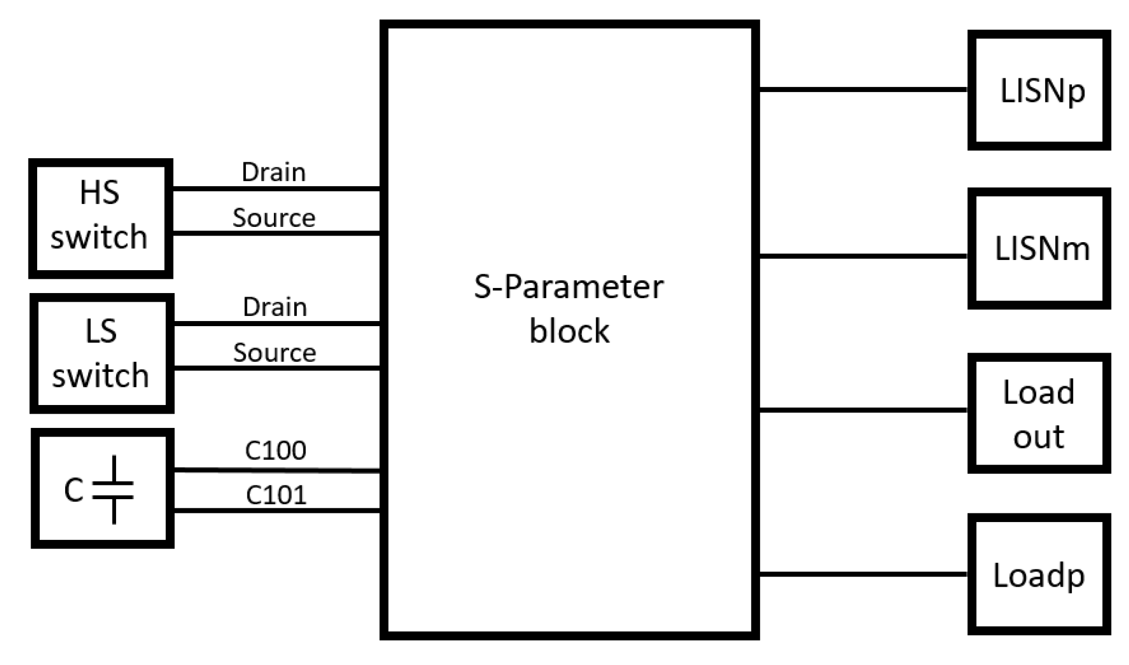
To facilitate detailed studies on the influence of the critical components (component group two) on the EMC characteristic, one can generate a multi-port S-Parameter model (Touchstone.SNP) of the PCB from the 3D simulation results in CST. This multi-port model approximates the electromagnetic behavior of the PCB (including component group one) between the defined ports very accurately within the specified frequency range. The advantage of multi-port models over 3D models is their significantly reduced computational time (2s), and one may connect arbitrary circuit models at the individual ports. The usage of such multi-port S-Parameter models and how they may be used to predict the conducted EMC behavior are discussed in the following section.
3.4. S-Parameter Model
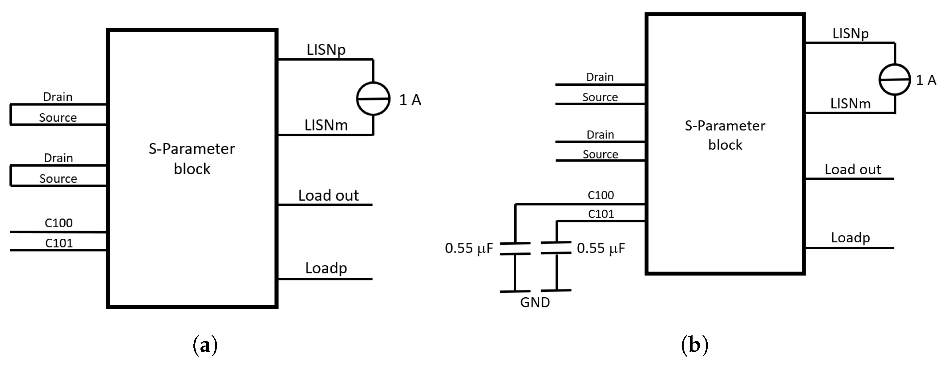
Figure 10 shows the extracted S-Parameter model from the 3D simulation results of the 3D model in
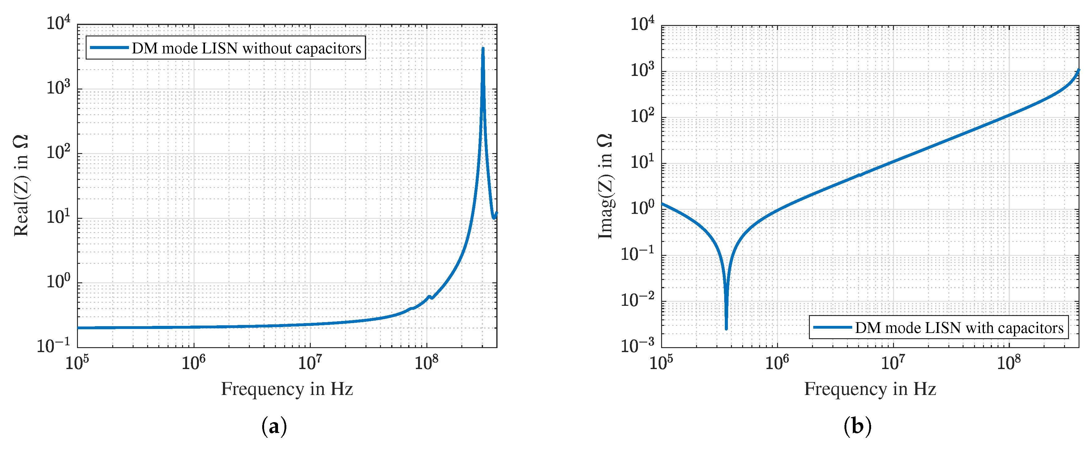
Figure 8. The 3D model has in total 10 face lumped ports; hence, the extracted S-Parameter model also has 10 ports where the external components, LISNs, and output load can be connected. Before one starts to connect all the components of interest to the S-Parameter model, it is important to validate its behavior by using AC simulations to avoid systematic errors. Therefore, we considered the following two test cases. First, the HS- and LS ports (drain, source) are shorted and a broadband AC current source with 1 A is connected between LISN P and LISN M (see
Figure 11a). The input impedance seen from the current source is analyzed, and since two 0.1
resistors are present in series (see
Figure 2), the resulting real part of the input impedance at low frequencies should be approx. 0.2
, which matches the simulation result in
Figure 12a. In the second test case, the capacitors
and
are connected to the S-Parameter model, while the same current source is connected between LISN P and LISN M (see
Figure 11b). The two capacitors have a value of 0.55
F at the given operation condition, and they are connected in parallel; hence, the resulting imaginary part of the input impedance at
f = 100 kHz should be approx. 1.5
, which also matches the simulation result (see
Figure 12b).
After validating the S-Parameter model, one is almost ready to simulate the conducted emissions of the test PCB. The final required step is the generation of a SPICE model from the S-Parameter block to enable transient simulations. This SPICE model can be generated by using the vector fitting feature in CST.
3.5. Vector Fitting
Because S-Parameters are frequency domain data, they can not be used directly for transient circuit simulations. In the past years, the vector fitting method has emerged as a powerful method to convert S-Parameter data into a passive and causal circuit ready for circuit simulation in the time domain [
6]. It has become a de facto standard for signal integrity simulations [
25], and we will also use this method for the application at hand. This methodology allows us to process the S-parameters and extract a corresponding reduced-order model by computing the state-space matrices A, B, C, and D. Computations of such matrices are performed by rational curve fitting. The model will be available in pole/residue form, and a realization process constructs the associated system of ODE’s in form of a state-space equation. Passivity enforcement is then applied to such state-space realization, and the final passive model can be then easily synthesized as an equivalent circuit ready to be used in any standard circuit simulation environment such as SPICE [
26]. The model generated by the vector fitting methodology allows us to directly apply arbitrary waveforms as excitations in a circuit simulation; thus, the impact of switching frequencies and switching slopes can be directly estimated.
However, the vector fitting process and the required passivisation step underlie certain inaccuracies that must be analyzed carefully to ensure reliable and accurate simulation results. During the fitting process, S-parameters at a fixed port reference impedance are fitted by iteratively increasing the number of poles until sufficient accuracy is obtained (an error criterion of 1 × 10⁻³ is recommended by the CST support). However, this accuracy is only maintained in the circuit simulation if the same impedances are used as loads in the time domain simulation. If the component models attached to the vector-fitted SPICE model have a frequency dependent impedance that significantly deviates from the impedance that was used in the fitting process, the fitting error might be amplified and lead to inaccurate results in the transient circuit simulation. Our tests have shown that this amplification is more probable with an increasing number of ports.
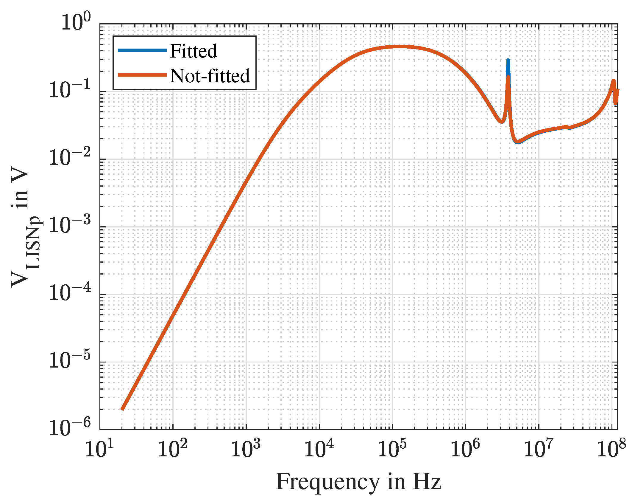
Therefore, we propose to test the fitting quality not only on individual S-Parameters but also on the system response. For the conducted emission simulations, the coupling from the noise source to the LISN is of interest. Hence, we set up a test-schematic that allows us to compare the transfer function from the transistor to the LISN ports for the unfitted and fitted case, see
Figure 13. To do so, an AC simulation is set up. In the AC simulation, a broadband 1V source is placed on the high side transistor, and the low side transistor is shorted. This setup creates a current loop through all components of the bridge and allows us to quantify the accuracy of the fitted model in system simulations.
Figure 14 depicts the comparison of the transfer function from the high side transistor to LISN P for the fitted and unfitted model. We observe great accuracy over the complete frequency band of interest. For clarity, only LISN P is plotted; however, the accuracy for LISN M was also checked.
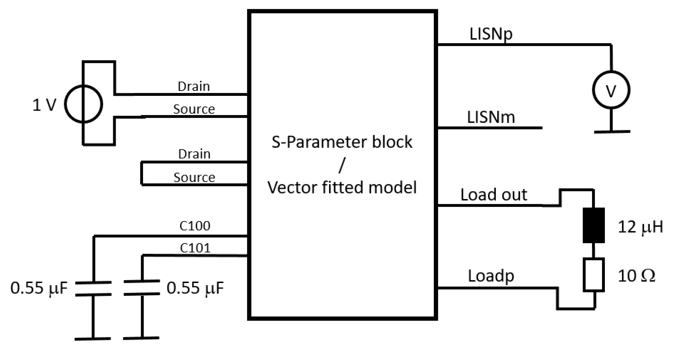
This vector-fitted SPICE model can now be used to perform system level simulations to predict the conducted EMC behavior of the complete test PCB comprising LS- and HS-switches, capacitors, LISNs, and output load.
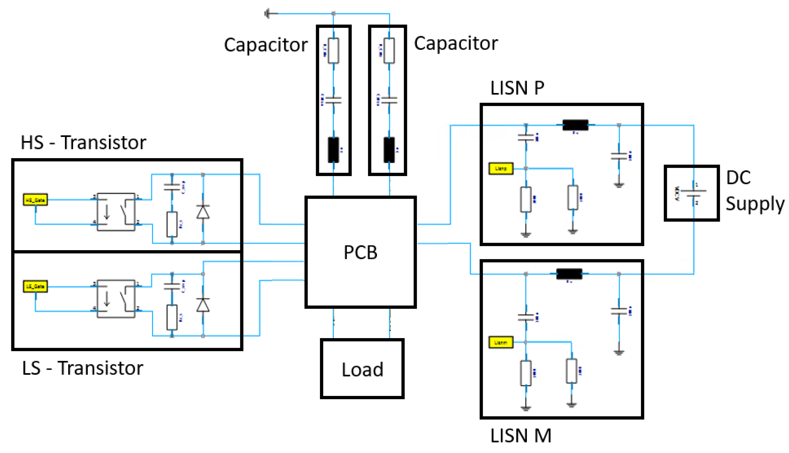
3.6. Assembly
This section describes the assembly of the complete test PCB, including circuit models for the mounted components, LISN, and the connected load (see
Figure 15). The external components are modeled with equivalent circuit models, and their parameter values are extracted from their datasheet if not stated differently.
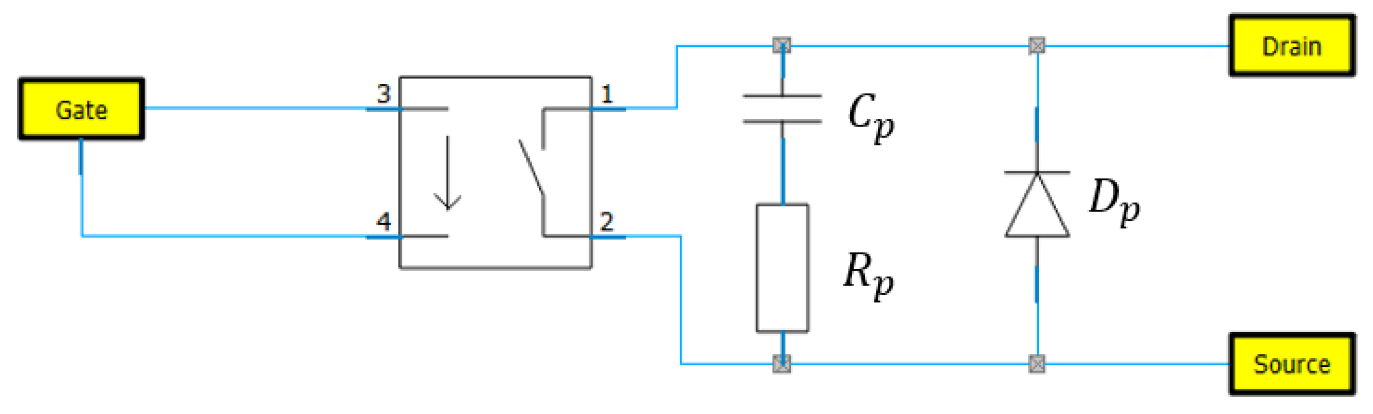
3.6.1. Transistor Model
The transistor is a critical component when the conducted emissions up to 400 MHz are of interest [
1]. Very often, there is no reliable transistor model available from the vendor; hence, one must develop a suitable model by oneself. The development of an accurate transistor model may be difficult due to the voltage-dependent non-linear effects and limited information in the datasheet. Therefore, a simplified equivalent circuit model of the mounted transistors is proposed which only considers the output characteristics between the drain and source. The electromagnetic coupling between the gate and drain/source is neglected in a first approximation.
Figure 16 depicts such an equivalent circuit model using an ideal switch with an on-resistance
, an output capacitance
, and a reverse diode
. The parameter values
= 70 m
,
= 200 pF, and
= 100 m
were taken from the datasheet provided by the vendor [
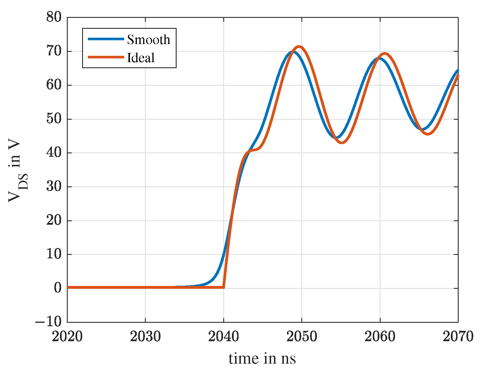
17]. One issue which arises by using this equivalent circuit transistor model is the high slew rate of the ideal switch when it is triggered (see
Figure 17). To overcome this issue, CST allows the definition of a transition width in the switch model to achieve a smoother switching behavior of the output [
12]. Another inaccuracy that must be considered when using the equivalent circuit model is the excessive current oscillation through the transistor model (drain current) when it is switched on, see
Figure 18. As shown in
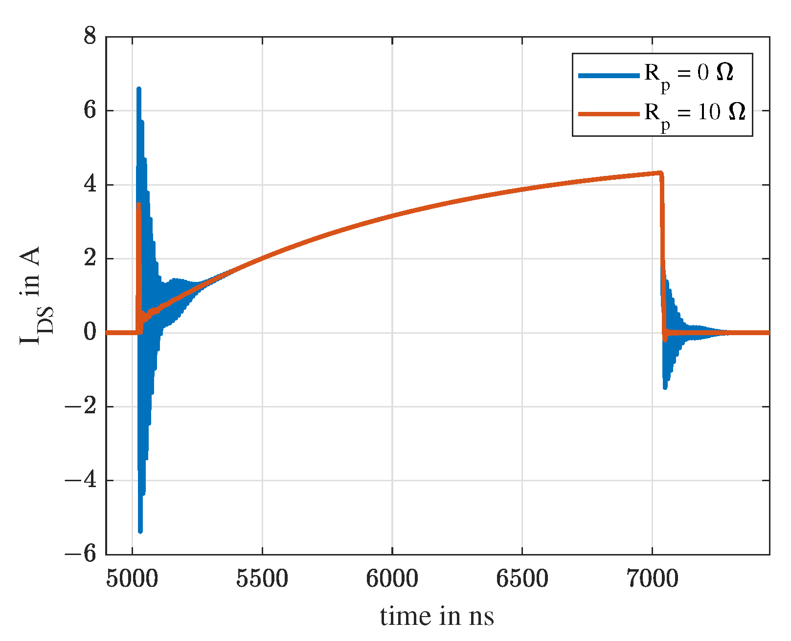
Section 4, these excessive currents lead to a significant overestimation of the conducted emissions at 82 MHz. Therefore, an additional resistor
is proposed that is placed in series to
to dampen the observed current overshoots. Reducing the current overshoots also reduces the simulated conducted emissions at 82 MHz, as shown later (see
Section 4). A value of
= 10
was chosen arbitrarily to overdamp the switching current, as shown in
Figure 18. The two values
= 0
and
= 10
are considered to investigate the impact of current overshoots on the conducted emissions. The simulation results indicate that the value of
should be voltage-dependent to model the transistor behavior at various supply voltages accurately. However, the development of a sophisticated transistor model, including voltage-dependent effects, is not within the scope of this work; rather, we aim to identify how to simplify its behavior to still obtain a reasonable approximation of the conducted emissions. The parameter values for the transistor model are summarized in
Table 3. We would like to point out once more that we do not consider voltage-dependent effects with our transistor model, only its switching characteristic.
3.6.2. DC Link Capacitors
Figure 19 depicts an equivalent circuit model of the DC link capacitors. The parameter values listed by
Table 4 reflect the typical characteristics obtained from the datasheet [
18]. Although the nominal capacitance of the used high-voltage-rated components is 1
F, it decreases to about 0.55
F at the low operation voltage used in this work.
3.6.3. LISN Model
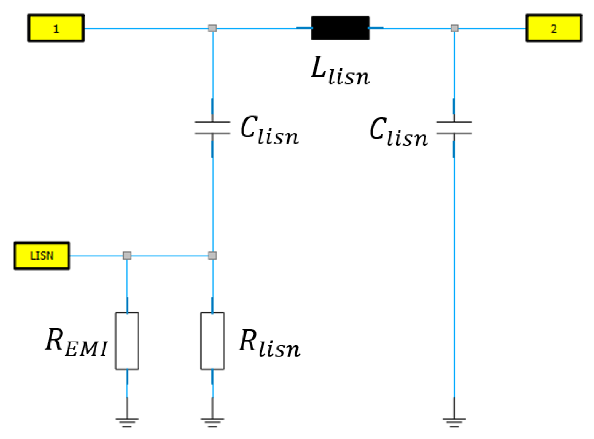
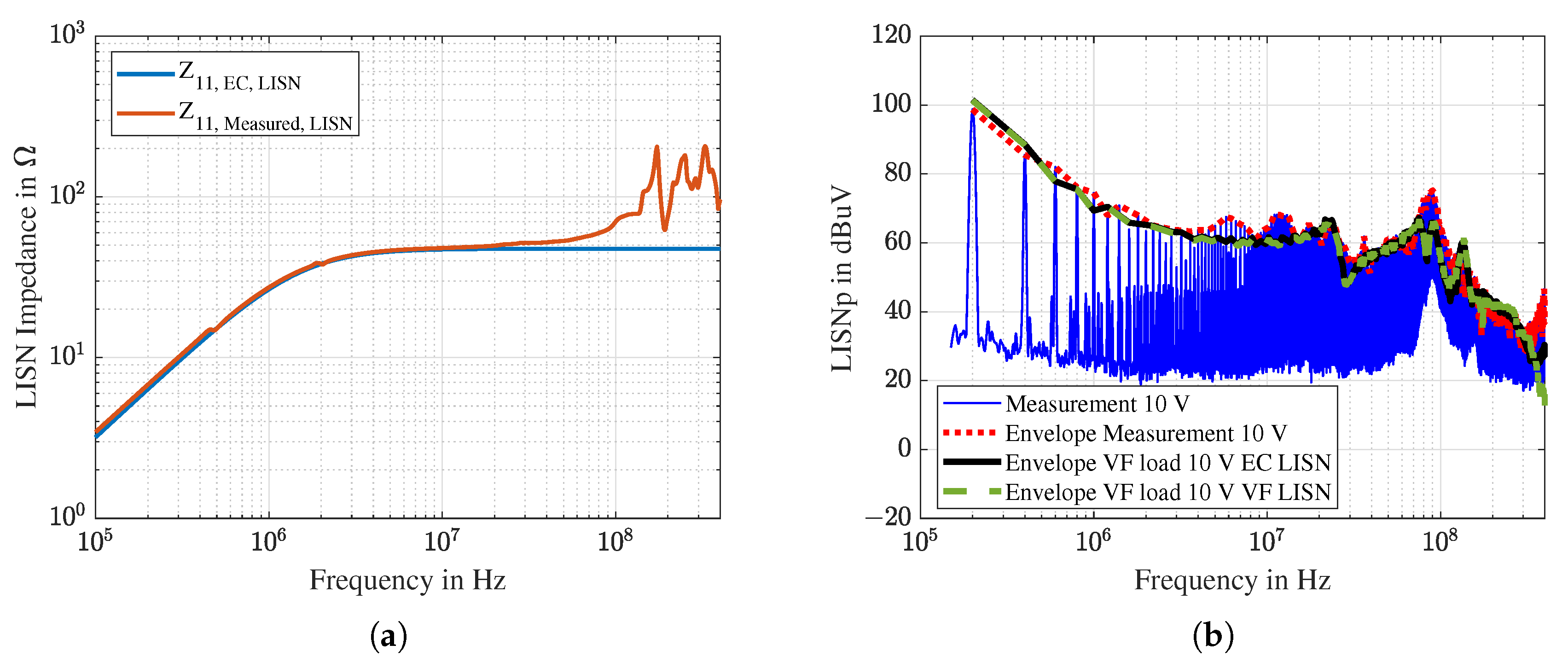
Figure 20 depicts an equivalent circuit model of the used LISNs [
19] which is validated up to 150 MHz. The resistor
describes the input and termination resistance of the connected measurement equipment, and the parameter values are summarized in
Table 5. Although the equivalent circuit model is only validated up to 150 MHz, it can still be used up to higher frequencies, as shown in
Figure 21.
Figure 21a compares the simulated and measured impedance at port 1 of the LISN. As shown, the measured impedance deviates from the simulated impedance above 100 MHz. However, this difference in the impedance characteristic does not have a significant impact on the overall conducted emissions, as shown in
Figure 21b. To obtain the simulation results in
Figure 21b, a vector-fitted SPICE model was extracted from three-port S-Parameter measurements and included in the assembly depicted in
Figure 15. Further details regarding the simulation setup are discussed in the next section.
3.6.4. Load Model
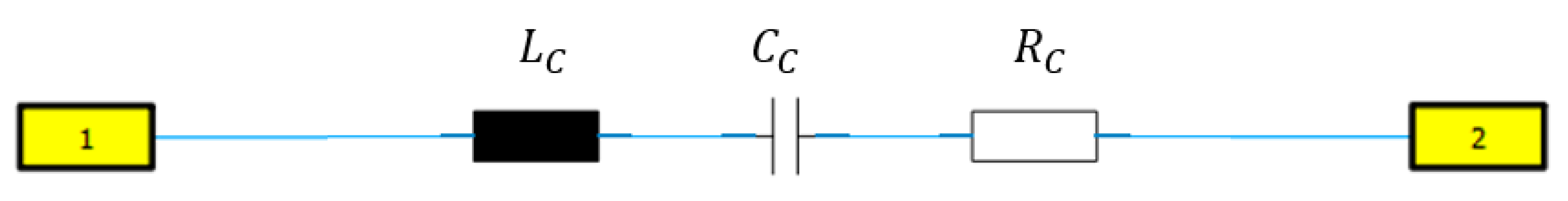
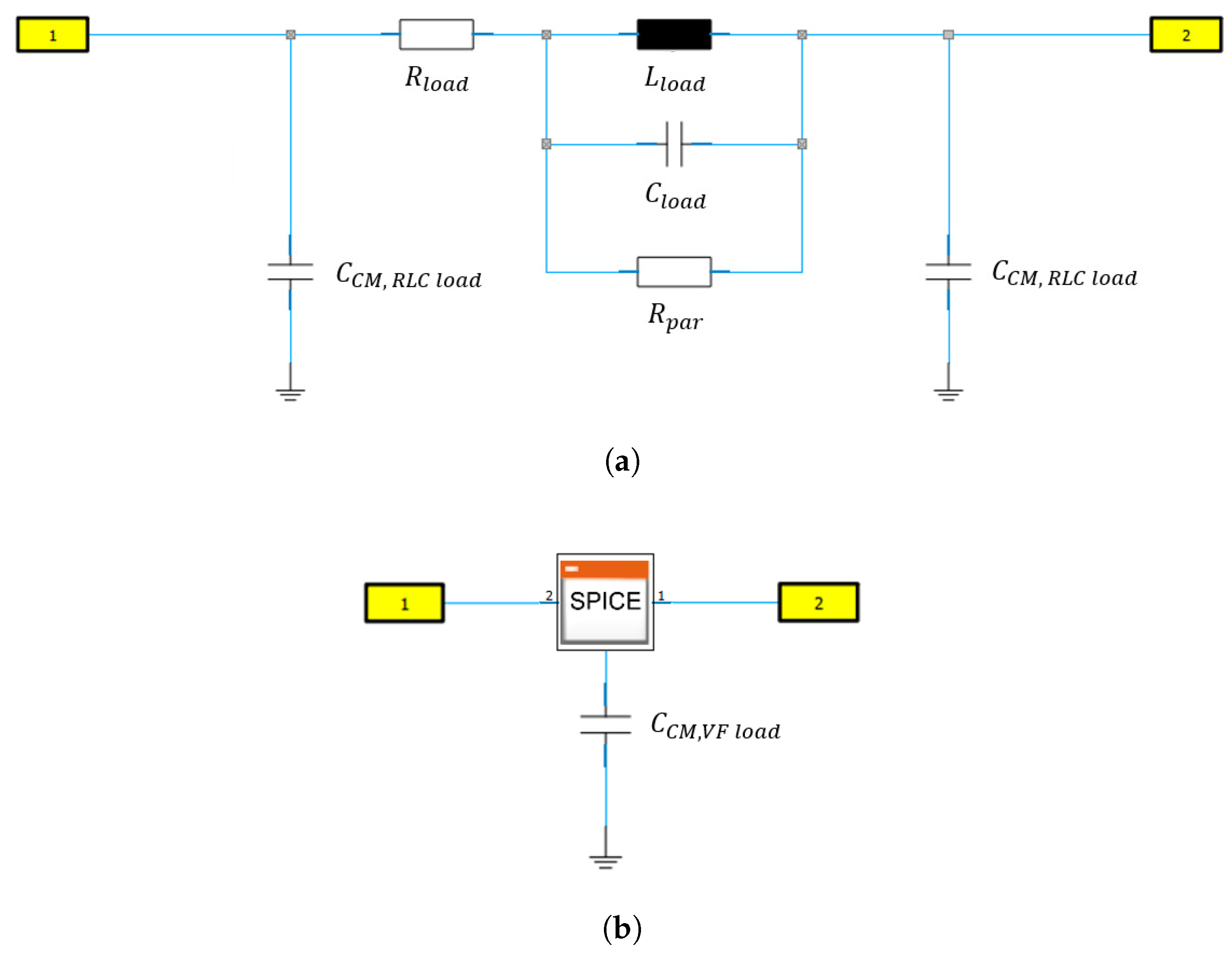
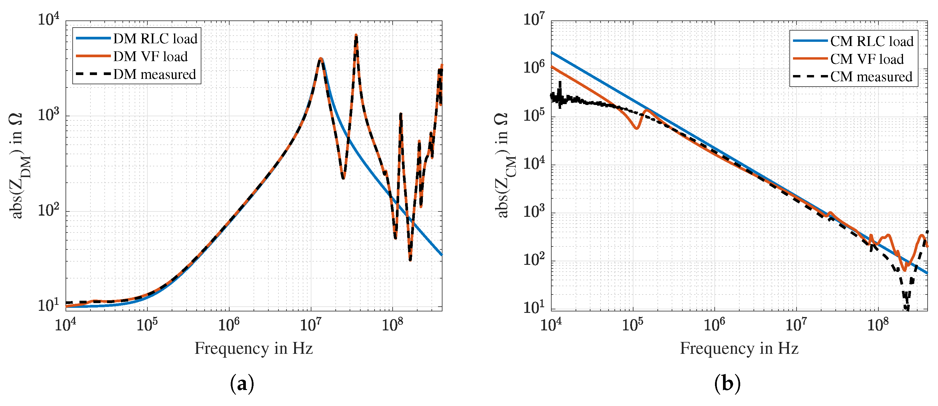
Figure 22 depicts two different equivalent circuit models of the load.
Figure 22a is a simple circuit model considering only the the load resistor
= 10
and the first parallel self resonance of the load inductor. The parameter values
= 12
H,
= 12 pF and
= 4000
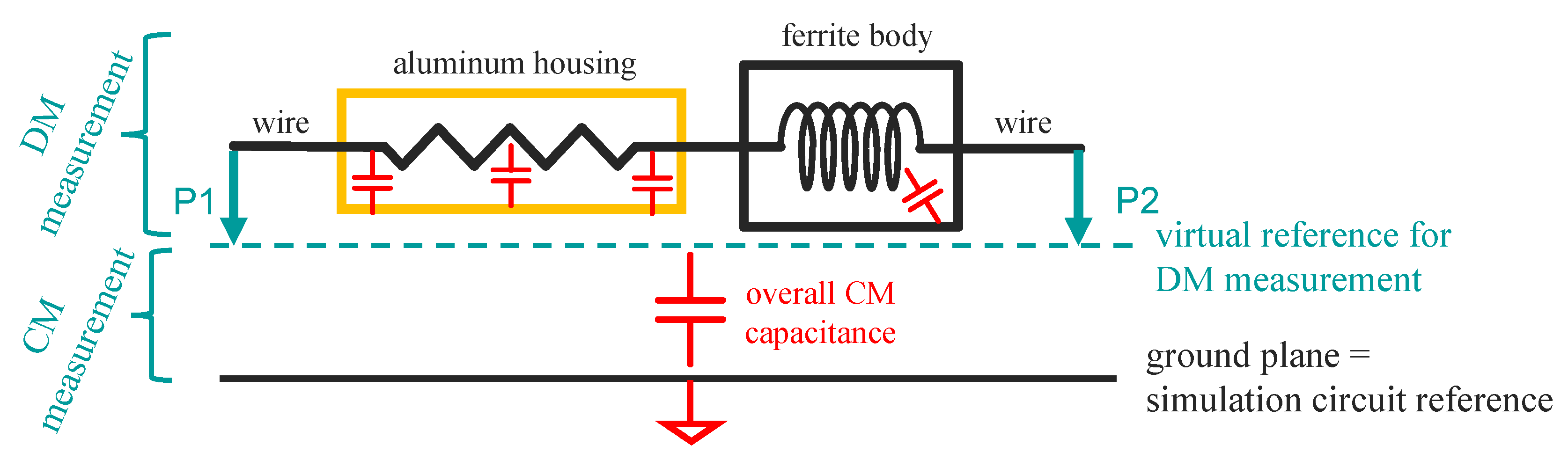
are extracted from the DM measurement depicted in
Figure 6a. The capacitance
= 3.6 pF describes the common-mode capacitance between load and metal table and is extracted from the CM measurement shown in
Figure 6b. The parameter values are summarized in
Table 6.
Figure 22b is an equivalent circuit model extracted from the DM measurement using vector fitting, as described in
Section 3.5. This approach provides a sophisticated load model; however, it requires suitable S-parameter raw data, i.e., a sufficient number of frequency points, low noise, etc., and thus careful measurement and potentially pre-processing. The capacitance
= 14.4 pF describes the common mode capacitance between load and metal table and is extracted from the CM measurement to fit the measured CM impedance above 1 MHz.
Figure 23a,b compare the DM and CM impedance of the RLC circuit model and the vector-fitted (VF) SPICE model to the measurement data.
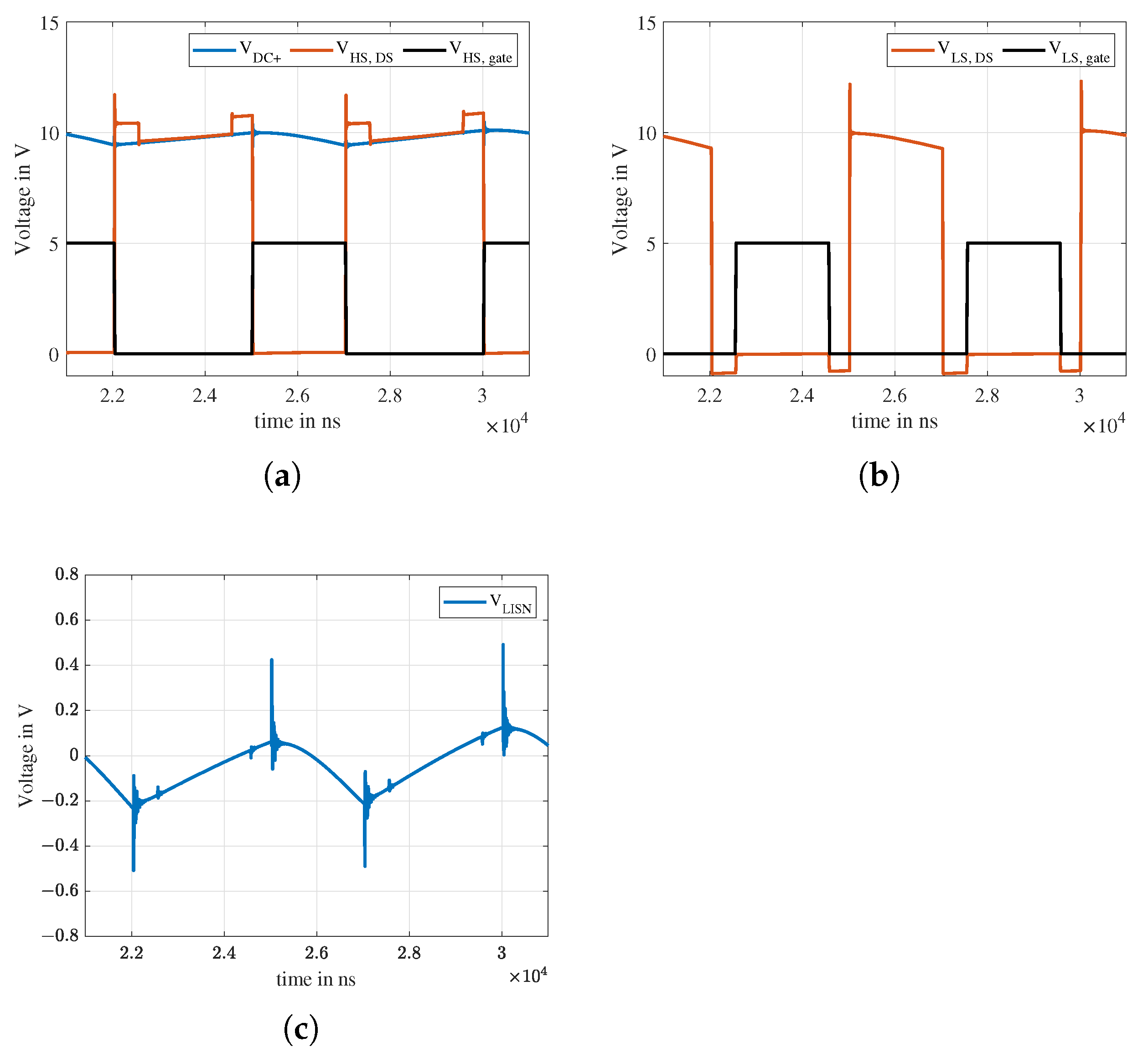
3.7. Time Domain Simulation
The time domain simulations of the assembly in
Figure 15 are performed in CST Design Studio and are based on a SPICE implementation. The simulation is set up with a duration of 1 ms to ensure that initial transient effects subside. A maximum frequency of
= 400 MHz and an adaptive time stepping are used in the transient simulator (
= 125 ns and
= 125 fs). The control voltage at the gate terminal of the transistor model uses an amplitude of 5 V, a frequency of 200 kHz and a duty cycle of 40% (compare
Figure 24). Furthermore, the halfbridge uses a break-before-make switching scheme, and hence a dead time of 500 ns is used. The resulting simulated switching behavior of the HS transistor, LS transistor, and the positive supply voltage
are shown in
Figure 24a,b. When the HS transistor is either switched on or off, a significant voltage spike can be observed at the output of LISN P (see
Figure 24c). Finally, to obtain the simulated conducted emissions at LISN P, an EMI receiver model [
27] is applied to
. The simulated and measured conducted emissions are compared in
Section 4.
3.8. Summary Workflow
The modeling workflow discussed above can be summarized into the following steps:
Import the odb++ database of the PCB into the CST Studio Suite.
Define surface lumped elements for all external components which:
and define their electrical R, L, and C behavior.
Define surface lumped ports for all external components that experience fast switching load currents.
Run 3D FEM simulations to obtain the S-Parameters of the defined ports and export the results into a S-Parameter model (Touchstone file). The usage of a direct solver is recommended to increase computational efficiency.
Validate the S-Parameter model using AC simulations.
Generate a SPICE model from the S-Parameter model by using vector fitting and monitor the fitting error.
Develop a suitable equivalent circuit model of the transistors, capacitors, and LISN.
Characterize the load in terms of differential mode and common mode measurements and extract:
Connect models of the transistor, capacitor, LISN, and load to the vector-fitted SPICE model of the PCB and run a transient simulation with the desired supply voltage and control signals.
Apply a suitable EMI receiver model to the transient simulation results to obtain your conducted EMC behavior.
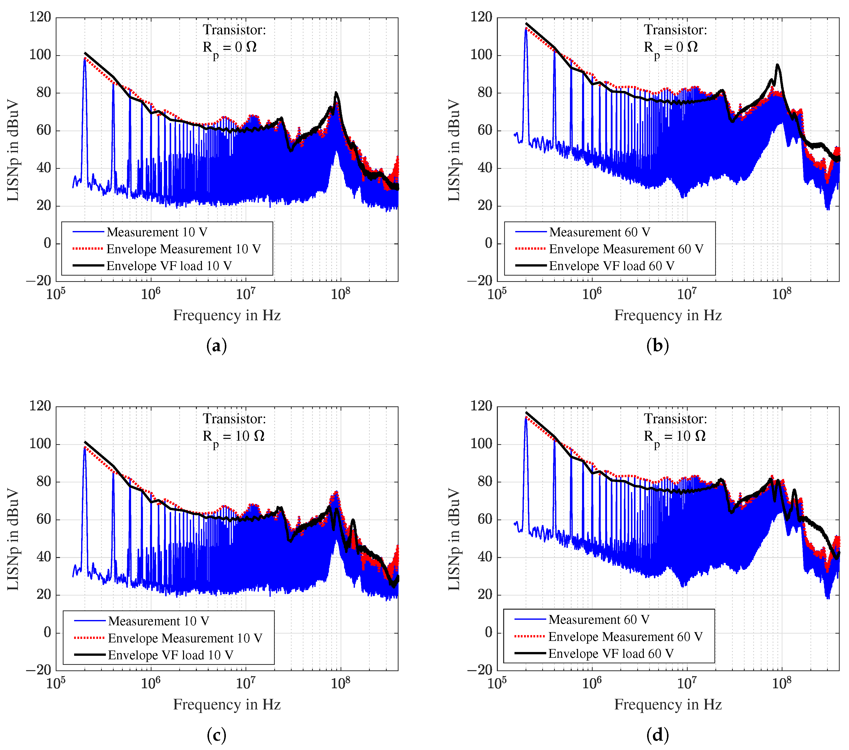
4. Results
Figure 25 and
Figure 26 depict the simulated and measured conducted emissions at port LISN P of the assembly shown in
Section 3.6. The simulation results were obtained by using DC power supplies of 10 V and 60 V when deploying the simplified RLC load model (see
Figure 22a) and the vector-fitted load model (see
Figure 22b).
Figure 25a,b show the simulation results for the simplified RLC load model and the transistor model with
= 0
. As shown, the simulated conducted emissions up to 3 MHz are in good agreement with the measurement, and the error is less than 5 dB for both supply voltages. As the supply voltage increases, the conducted emissions also increase (approx. 15 dB) due to a higher current through the load. From 3–30 MHz, the simulation slightly underestimates the emissions but the difference is less than 12 dB. At 82 MHz/60 V (see
Figure 25b) the emissions are significantly overestimated (approx. 18 dB). These excessive emissions are caused by the transistor model due to its current overshoots when
= 0
(see
Figure 18). Changing the value of
to 10
reduces these current overshoots; hence, the model can be improved at 82 MHz, as shown in
Figure 25c,d (error < 12 dB). Furthermore, we would like to point out that changing the value of
only affects the emissions peak at 82 MHz, whereas the emissions at other frequencies do not change (compare
Figure 25).
Using the simplified RLC load model already leads to a good agreement between simulation and measurement, especially if we consider the simplicity of the load- and transistor model. The difference between simulation and measurement does not exceed 5 dB up to 3 MHz and 12 dB from 3–400 MHz, respectively. However, the accuracy can be further improved by using the discussed vector-fitted load model.
Figure 26a,b show the simulation results for the vector-fitted load model and the transistor model with
= 0
. As shown, the accuracy of the simulated emissions from 3 MHz–60 MHz improves significantly (error < 7 dB) compared to
Figure 25c,d. However, the vector-fitted load model still overestimates the emissions at 90 MHz/60 V, see
Figure 26b. Changing the value of
to 10
suppresses these excessive emissions (see
Figure 26d), leading to a good agreement between simulation and measurement up to 170 MHz (error < 7 dB). For frequencies above 170 MHz, both values for
(0
, 10
) lead to an overestimation of the emissions (approx. 12 dB). This issue may be explained by the simplified transistor model using a fixed value for
that does not consider any voltage-dependent effects since the simulated emissions are in excellent agreement with the measurement when a DC supply voltage of 10 V is applied (see
Figure 26a,c).
5. Discussion
This paper presented a modeling workflow for simulating the conducted emissions of a power electronic system using a halfbridge circuit to switch an inductive load at its output. The methodology combines 3D FEM simulations, measurements, and SPICE circuit simulations to consider the electromagnetic parasitic effects introduced by the PCB, components, and load. It was shown that a simple equivalent circuit transistor model that only considers its output characteristic (drain-source) is suitable to approximate its conducted emission behavior up to 400 MHz with an accuracy of 12 dB. Furthermore, a simple equivalent circuit model of the LISN network which is validated up to 150 MHz was deployed up to 400 MHz, and hardly any impact on the overall conducted emissions accuracy was observed. The obtained simulation results are in good agreement with measurements, especially if one considers the simplicity of the used transistor and load models. The presented approach does not require a physical demonstrator to fit model parameters; therefore, one may use this approach to approximate the conducted emissions of a power electronic system up to 170 MHz with an accuracy of 7 dB and above 170 MHz with an accuracy of 12 dB. Certain inaccuracies could be observed especially between 3 and 20 MHz and above 170 MHz/60 V. From 3–20 MHz, the conducted emissions are slightly underestimated (approx. 7 dB), but it is presumed that this issue arises due to measurement inaccuracies in the CM measurement. The measured CM load impedance, and hence the extracted CM load capacitance , is very sensitive to parasitics introduced by the measurement setup due to its small value (few pF). Changing the value of also changes the simulated emissions from 3–20 MHz. Therefore, we expect a model improvement when the accuracy of the CM measurement is increased. The simulated conducted emissions above 170 MHz for a DC power supply of 60 V are overestimated by approx. 12 dB due to the simplified transistor model neglecting voltage-dependant effects.

 ,
, 


