Article

Time–Frequency Analysis of Experimental Measurements for the Determination of EMI Noise Generators in Power Converters

Electronics and Computer Science Department, Faculty of Engineering, Mondragon Unibertsitatea, 20500 Arrasate-Mondragon, Spain
*
Author to whom correspondence should be addressed.
Electronics 2022, 11(23), 3898; https://doi.org/10.3390/electronics11233898
Submission received: 28 October 2022 / Revised: 18 November 2022 / Accepted: 22 November 2022 / Published: 25 November 2022
(This article belongs to the Special Issue Electromagnetic Interference, Compatibility and Applications)

Abstract

:
In the context of recent decades in which there has been great development in power electronics systems with increasingly better operating characteristics, the study of the factors that affect the behaviour of these systems in terms of electromagnetic interference (EMI) is mandatory. Within this general perspective, it is essential to know the time and frequency characteristics of the switching signals, as they are the main sources of EMI noise. This work analyses the suitability of different spectral analysis techniques, specifically short-time Fourier transform (STFT) and continuous wavelet transform (CWT), to extract the frequency characteristics of the switching signals of a converter. Thus, a test bench based on a half-bridge was designed as a preliminary step in the development of a model of noise generators. After the analysis of the main parameters of these techniques, a comparison of the results obtained was carried out. It was concluded that both techniques are considered valid and complementary; not only that, but they overcome some limitations of the fast Fourier transform (FFT) as they offer the possibility of determining which are the frequency components associated with different types of events occurring at different times.

1. Introduction

Power electronic devices are intrinsic generators of electromagnetic noise and interference when operating in switching conditions, ultimately resulting in both conducted and radiated emissions. The study of these phenomena has been and still is widely discussed in the literature from different points of view involving the elements represented in Figure 1, such as EMI sources, common and differential mode propagation paths, EMI modelling techniques, EMI attenuation/cancellation procedures, measurement techniques, EMC regulations, etc.
Starting with noise generation, the literature [1,2,3,4,5] in recent decades has extensively reported that these noise sources are mainly caused by two reasons: on the one hand, the rapid voltage and current variations ( d v / d t and d i / d t ) that occur during the turn on and turn off of transistors; on the other hand, the oscillations produced by the excitation of the intrinsic parasitics of the semiconductors and the parasitics associated with the layout of the circuits or the different types of couplings (mainly capacitive).
Although this topic has been widely covered for years, the evolution of power semiconductors (transition from silicon-based devices to WBG semiconductor-based devices) and the variation of operating conditions in characteristics such as switching frequency, speed or operating voltage (evolution towards higher values) have made it necessary to continue to study these phenomena in all of the above-mentioned areas [6,7,8,9,10].
This is part of the general objective of system modelling, which is still relevant today when dealing with problems and associated applications such as the derivation of the EMI model itself [11], the separation of common-mode and differential-mode noise [12], the EMI filter design [13,14,15], etc.
Within this general issue and regarding the further goal of modelling the system, a key aspect is to relate time and frequency, both at the point of EMI noise generation and at the EMI/EMC noise measurement points; ultimately, the events occur in time, but the EMI/EMC measurements express power in the frequency domain.
This study of the time–frequency characteristics of the signals of interest can be carried out in different ways.
Obtaining the signals in the time domain involves modelling the semiconductors and analysing the PCB layout with simulators and parasitic extraction tools, and the use of analytical models, circuit models, etc. Using these methods, very high levels of detail can be obtained; this works in their favour, but these models are difficult to parameterise and simulate [16,17,18,19,20,21] and are highly dependent on the layout. Another option, also widely reported in the literature, is to obtain the most relevant switching waveforms experimentally. A sine qua non for using this method is that the measured signals can reflect the switching result as faithfully as possible, without being affected by the characteristics or limitations of the measurement system itself. This factor has become increasingly relevant for semiconductors operating at higher and higher frequencies and switching speeds.
However, obtaining the time signals is only the first step, as spectral analysis and performing this time–frequency correlation is not as immediate as it may seem at first glance due to the characteristics of the switching signal. The literature reports in [22,23,24,25] that it might not be enough to apply the Fourier transform in some of its implementations (such as the fast Fourier transform or FFT) to obtain the frequency response of the noise generators. These generators, together with the propagation paths, will allow the establishment of a model that links input and output. The model will relate the signals provided by the noise sources due to the switching and the results obtained from the conducted emission and radiated emission measurements in the corresponding time or frequency domain.
Among the existing options, this work proposes to obtain switching signals experimentally and, from them, to calculate their spectrum, pursuing three main contributions to the current state of the art:
(1)
To measure the voltage and current signals characteristic of semiconductors by selecting the appropriate measuring instruments (voltage and current probes, oscilloscope and spectrum analyser) and establish a methodology for carrying out these experimental measurements with sufficient fidelity or resolution to be able to combine low switching frequencies with the observation of high-frequency phenomena responsible for the generation of EMI;
(2)
Obtain the spectrum from the complete experimental signals instead of obtaining the spectrum as the sum of individual time signal effects (switching slope, reverse recovery current, ringing, etc.). This can be considered one of the main gaps because, although there are authors who mention the existence of oscillations that give rise to peaks in the spectrum, these considerations are made only theoretically [26] or without clearly explaining how the signal is decomposed [27].
(3)
Analyse whether spectral analysis techniques other than the commonly used FFT are able to establish a one-to-one relationship between the characteristic time events of the switching signals and their corresponding spectra. Although techniques such as the short-time Fourier transform (STFT) or the continuous wavelet transform (CWT) are widely known by researchers in the field of signal processing, their application to the world of power electronics is more limited, and only a few examples can be found in the literature, as will be mentioned in Section 2.2.
For all this, a test bench was designed consisting of a half-bridge made up of two transistors, to which elements for measuring current and voltage were coupled.
The ultimate goal, as will be highlighted in the conclusions and future work section, is to offer power electronics engineers the possibility to predict what their noise generators will be before any conducted or radiated emission measurements are made, anticipate potential problems and design attenuation or cancellation measures by acting on those particular noise sources.
In the following sections, the steps followed to achieve this objective are presented. Thus, in Section 2, an overview of the general characteristics of the current and voltage switching signals and their spectrum will be given. At the same time, it reviews the STFT and CWT techniques and their main configuration options or parameters for obtaining the spectrum for signals with the particularities or characteristics of our switching waves. The knowledge of these characteristics is essential to plan the experimental measurements to be performed and select the appropriate equipment and methodology for those measurements, as explained in Section 3. Finally, taking into account the basics and criteria established in the previous sections, Section 4 includes the experimental work carried out, starting with the acquisition of the switching signals and concluding with their spectral analysis by means of STFT and CWT. The results of the analysis are presented in Section 4. Finally, Section 5 summarizes the conclusions drawn from the work carried out and proposes the next steps to be taken in this research.

2. Overview of the Time–Frequency Characteristics of Switching Signals and Spectrum Analysis Techniques

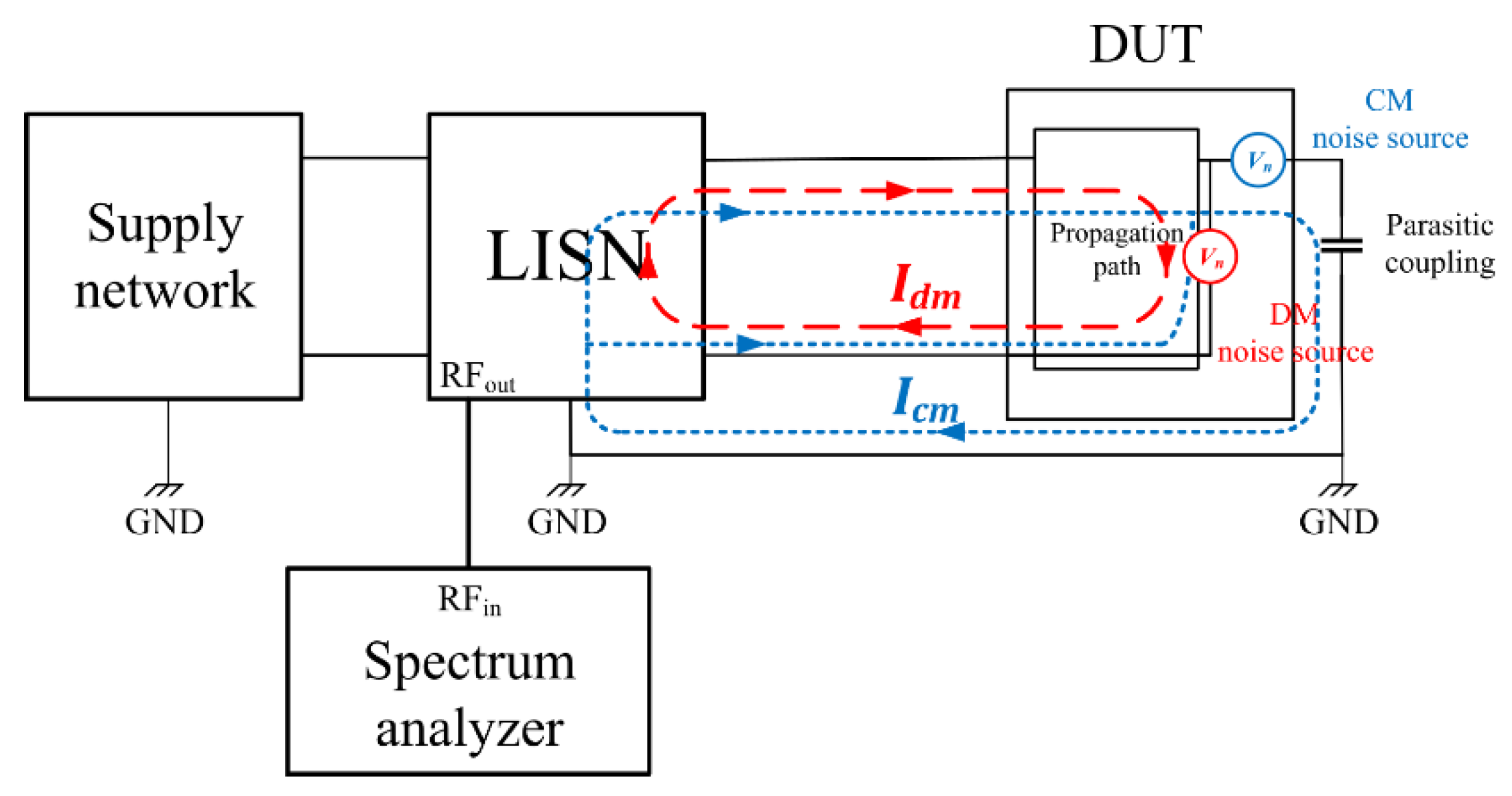
2.1. Time–Frequency Characteristics of Switching Signals

Several authors define the waveforms that are generated in the on and off switching of semiconductors, taking into account to a greater or lesser extent the associated parasitics: Ref. [28] describe those waveforms as piecewise defined functions; Ref. [8,10] propose analytical models in which they take into account high frequency parasitic effects; Ref. [7] model the switching by means of equivalent circuits, including parasitics and considering the oscillations produced due to them; Ref. [29,30,31] analyse the switching experimentally, etc.
In all cases reviewed from the literature, the waveforms of interest are the drain current ( I d ), the drain-source voltage ( V d s ) and the gate-source voltage ( V g s ); these are also the most relevant waveforms from the point of view of EMI generation. This is why they were chosen as test points for the experimental measurements (for the current measurement, which will be made with a coaxial shunt, source current I s was selected instead of I d , and the drain current will be obtained indirectly when calculating the noise sources in the equivalent circuit). This is not to say that this is the only information needed to fully represent the EMI characteristics, as the level of interference will vary across the PCB depending on other parameters such as the track geometry, routing way, presence of discontinuities, etc. In the model to be proposed in our future work, which remains pending in this article, these external effects will be taken into account through the characterisation of the propagation paths.
Whether by any of the above-mentioned methods, and even if some particularities are present depending on the type of transistor used, it is a practically unanimous convention [8,9,10,28,29,30,32,33] to define the switching process as a sequence of phases whose simplified form can be seen summarised in Figure 2.
It is also worth mentioning one of the effects reported in the literature such as false turn-on (also known as low-side false turn-on, dv/dt-induced false turn-on or cross-talk) where the active switch of the switching branch turns on and, in turn, the displacement current through the Miller capacitance ( C g d ) can cause the gate-source voltage to exceed the turn-on threshold value of the transistor in the lower part of the switching branch. Consequently, this also turns on, causing a short-circuit in that branch with the consequences that this entails such as losses and the possibility of damaging the transistors due to the large values of overcurrent that can be produced.
In order to analyse the spectrum of these switching waves, the transition between ON and OFF (or vice versa) can be roughly considered as a constant slope (determined by the transition time: rise or fall time). In this way, all these switching waves can be likened to trapezoidal signals, whose spectrum is determined by:
V ( f ) = 2 A τ T | sin ( π f τ ) π f τ | | sin ( π f t r ) π f τ | ,
where the magnitude of the spectrum and the cut-off frequencies or inflection points where the envelope slope varies are fixed by the signal amplitude (A), rise and fall time ( t r ), period (T) and pulse width (τ). Figure 3. shows the spectrum and envelope of a basic trapezoidal switching waveform.
On this basic shape several authors try to add to the basic or simplified temporal waveform the effects of resonances caused by the excitation of parasites [26,27,34] or effects that may occur such as cross-talk or false turn-on [35] and to see their translation both in time (overshoots and ringings) and in frequency (appearance of peaks in the spectrum).
In particular, Ref. [36] propose a graphical method to calculate the spectrum envelope asymptotically but limit the application to simple examples such as a square wave or smoothing function.
Middlestaedt et al. in [37,38] analyse the turn-on and turn-off transient of a MOSFET separately and relate it to its radiation characteristics but do so through the use of the FFT, which is discouraged in the literature for the case of nonstationary signals and obtaining a qualitative analysis of the spectral characteristics. Something similar occurs in the case of [34], which relates the ringing in the time-switched signals to the frequencies through experimental measurements made with an oscilloscope, implying that this spectral analysis is carried out directly with the oscilloscope using the FFT.
On the other hand, Ref. [26] includes in its spectral representation the effect of ringing in the voltage signal, but this is a simulation. The authors of [27] decompose the switching signal into a basic trapezoidal wave plus two adjacent effects (ZVS and ringing) but do so only in the case of the voltage between the drain and source, and it is not clear how this decomposition is performed and subsequently results in the spectrum.
Finally, Ref. [35] refers to one of the phenomena that can occur during switching, such as cross-talk or false turn-on but only analyses them in the time domain, without evaluating their impact on the spectrum. Against the background of the importance of large voltage and current variations in the generation of EMI, it is presumed that the occurrence of a false turn-on case is likely to trigger a higher level of conducted and/or radiated emissions. It is also considered a case of particular interest, given that the proliferation of WBG semiconductor-based systems may make this phenomenon more frequent (due to the higher values of d v / d t , which cause the effect).
It is, therefore, necessary to identify as precisely as possible the different phenomena that occur during transistor switching, and spectral analysis techniques are needed to establish a precise correlation between time events and their frequency correspondence. This aspect will be dealt with in the following sections.

2.2. Spectrum Analysis Techniques

As indicated in the previous subsection, several authors relate the signals obtained in time with the spectrum associated with them.
When obtaining the spectrum of the measured time signals, the basic tool is the Fourier transform. However, we could say that this is governed by Heisenberg’s uncertainty principle (the absolute, theoretical limit on the combined accuracy of certain pairs of simultaneous, related measurements). Translated to our case, it means that it is impossible to relate the frequency components obtained as a result of the transform with precise time instants (in other words, it is impossible for the Fourier transform to locate the signals in time).
As [39,40,41] point out, this is a problem in the analysis of nonstationary signals. This is the case in our study, where impulsive and oscillatory components are added to the base spectrum of the switching signals of transistors. The literature discusses the use of other techniques to overcome this drawback. Two of the main techniques are the use of STFT and wavelets.
The STFT consists of performing a set of Fourier transforms on the original signal subjected to an enveloping process, with a time t between each operation, which can be expressed mathematically as follows:
f ( t , ω ) = f ( t ) w ( t τ ) e j ω τ d t ,
where f ( t ) is the original signal, w ( t ) is the applied window and t is the offset. At each signal slice affected by the window, the signal is considered to be stationary. Thus, the STFT results in a kind of sliding window FFT, with the resulting spectrum characterised by effects such as coherent attenuation, scallop loss and leakage [22].
As pointed out by Sandrolini in [41], in this operation, the choice of the window and its associated parameters (both its duration and shape) is key, as it needs to reach a compromise solution between achieving better frequency resolution at the cost of having a higher ripple (with rectangular windows) or a worse frequency resolution but with less lateral oscillations in the spectrum. It also needs to determine the optimal window that correctly describes the frequency and amplitude [42].
The length of the window T will determine the frequency resolution or bin size Δ f = 1 / T , which, in turn, relates to the number of points represented through the sampling frequency, f s = N · Δ f .
Examples of applications can be found, such as the spectral estimation and emulation of EMI receivers [22,41,43,44], measurement of electrical signal quality in power systems, fault detection in photovoltaic systems [45] and conducted emissions analysis on DC-DC buck converters [46].
Therefore, the STFT is presented as a tool that allows the time–frequency indeterminacy mentioned above to be overcome, but, even so, it suffers from a fixed resolution; that is, once window is selected, the temporal and frequency resolution remains fixed, which implies that a window of longer duration has problems representing events of a short duration and vice versa.
A possible solution to this problem can be using wavelets. Wavelet analysis involves the use of a basis function for wrapping called the mother wavelet, whose scale is changed, shifted in time, multiplied by the signal and integrated in time. Mathematically, it can be expressed as:
X C W T   ( p , q )   =   x ( t ) ψ τ , a * ( t ) d t ,
where X C W T   ( τ , a ) are the coefficients obtained for a translation τ and a scale a of the mother function ψ τ , a , so that:
ψ τ , a = 1 a ψ ( t τ a ) ,
As a result, detail is obtained on the frequency components of the signal in a time interval allowing a time–frequency “cross” localisation [25]. Unlike STFT, it is a multi-resolution tool, i.e., by compressing or “stretching” the wavelet function (with a variable length window, if we use terms analogous to those of STFT), a compromise between temporal and frequency resolution is achieved for the entire spectrum.
As in the case of the STFT, wavelets have found diverse fields of application such as in the health sector with the processing of biomedical brain, cardiac and muscular signals [47], transients in power systems [24,48], seismic phenomena, and condition-monitoring within an inverter [49].
Both analyses are compared in [42,43,50], highlighting the pros and cons of each and basically reaching the conclusion that wavelets have advantages when the frequency characteristics of the signal vary rapidly with time, whereas STFT has advantages at a computational level if real-time analysis is necessary.
In any case, both techniques can be complementary, and in this paper, both techniques were applied to the experimentally obtained switching signals by performing the analysis with different parameters with the double objective of identifying the fundamental components of the spectrum and relating them to the events in the switching signals as a first step to obtain the modelling of the noise sources as a set of series generators.

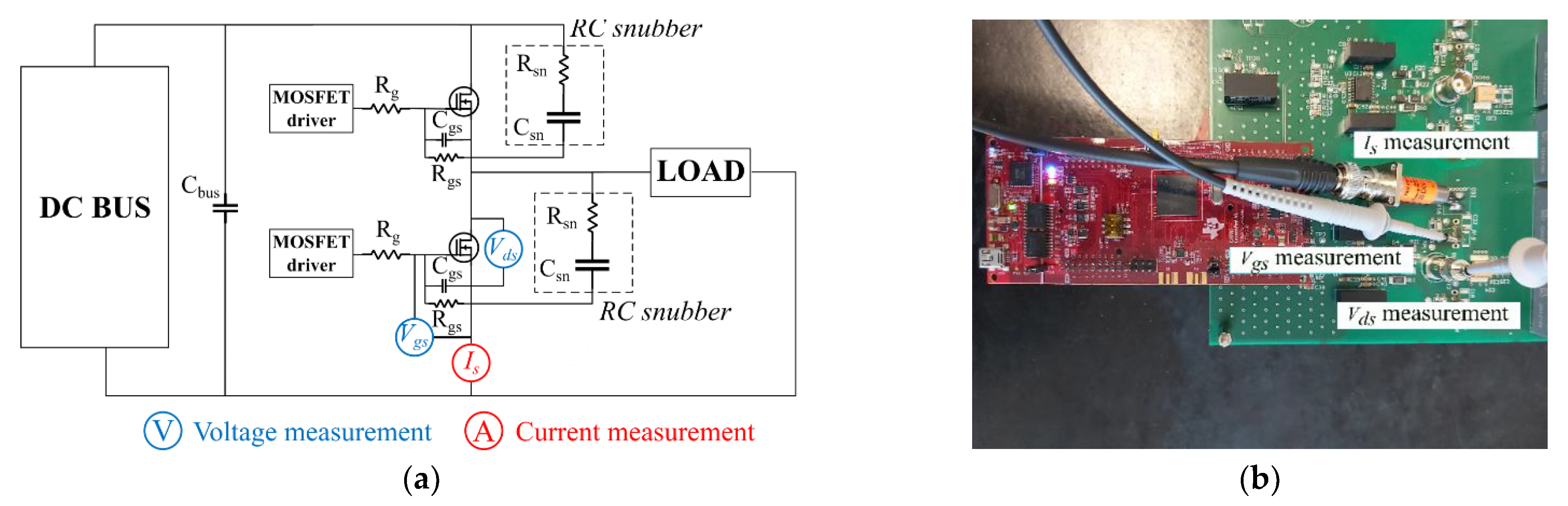
3. Materials and Methods for Switching Waveforms Measurement

As noted in the introduction, one of the objectives is the definition of noise generators based on the experimental measurement of switching waves. In anticipation of the growing need to measure not only faster and faster transients but also oscillations or ringings that have higher frequency components than the previous ones, the specifications required for the probes are increasingly stringent in terms of parameters such as bandwidth and load introduced into the layout in the form of parasitics [51,52,53].
Although a number of characteristics are general, it is useful to differentiate, as is performed in the literature, between voltage and current probes.
For voltage probes, two of the most important features to take into account are the maximum voltage at which they can work (dynamic range) and the bandwidth (related to the rise time) [51].
In the comparison between differential and passive probes, differential probes, which provide galvanic isolation, have been preferred in the case of having to measure voltages of the order of kV; on the other hand, their limited bandwidth, coupled with their high price, makes them undesirable for our goal, i.e., to detect the rapid variations in signal that can lead to EMI phenomena. In our case, having to measure up to a few hundred volts (typically 300 V) and taking into account that they are more suitable for higher bandwidths, passive probes are preferred.
Even so, in the case of passive voltage probes, it is essential to be able to dispense with the ground lead, as this cable introduces additional inductance that can cause overvoltage and ringing [54].
As far as current probes are concerned, Rogowski coils, Pearson current transformers and coaxial shunts are common alternatives. The first two are more limited in terms of bandwidth (typically tens of MHz, which implies a rise time of tens of ns), so they may not be suitable for measuring faster signals [51,55].
Current shunts show better bandwidth characteristics at the cost of lacking galvanic isolation. Furthermore, as they are inserted directly into the circuit layout, it is a challenge, as [56] points out, to measure current without introducing additional inductance into the switching loop, as this contribution is the major influence on the generation of overshoot and ringing that will lead to EMI. All these characteristics are summarised in Table 1.
On the other hand, as mentioned in Section 1, a test bench was designed based on a half-bridge whose simplified diagram is shown in Figure 4a and which focuses on 3 aspects: the PCB design, the parameter sensitivity, and the instrumentation and techniques needed to measure EMI.
For voltage measurements, PML 711A passive probes with a bandwidth of 500 MHz and an input capacitance of 9.5 pF were selected to minimise the load on the circuit, and they have a 2.5 mm housing to facilitate access to components on the PCB. In order to take simultaneous measurements of V g s and V d s , bearing in mind that both measurements must have a common point (as we are working with passive probes and not differential probes), we chose to take one of the measurements using the BNC-tip adapter and the other using the ground clip attached to probe ground sleeve. In this way, the loop inductance is minimised.
In this case, some additional features such as the possibility of deskewing are not mandatory, as no losses are to be measured, so the synchronisation or V-I alignment characteristics voltage/current of the measurement is not mandatory.
On the other hand, a coaxial shunt (SDN-414-25) with a bandwidth of 500 MHz was selected to measure the current flowing through the MOSFETs. Before mounting it on the converter, the effect of the parasitic inductance introduced by the shunt coaxial itself, due to its 1” (2.54 cm) long pads, was analysed.
This current sensor was characterised in the conducted emission range using a Bode 100 impedance analyser for both the original sensor and a modified version resulting from shortening its pads (Figure 5a), with the results shown in Figure 5b.
It can be seen that, as expected, the impedance value is more affected in the case of the original shunt coaxial by the inductance introduced by the terminals. Calculating the fitting curve to consider a linear variation with frequency, the inductance value obtained is 3 nH for the modified sensor, compared to 9 nH for the original sensor, which will be a benefit when introducing the lowest possible inductance in the overall computation of the parasitic inductance introduced by the semiconductors plus that of the tracks associated with the switching loop.
The characteristic switching signals of the transistors were measured for different cases to analyse the parameter sensitivity. In all cases, the measurements were made with an R&S RTO2014 oscilloscope with a sampling period T s = 2 · 10 10 s, so that the limiting factor in terms of bandwidth was derived from the current probes and the voltage probe, and not the oscilloscope.

4. Experimental Measurements and Spectrum Analysis Results

4.1. PCB and Measurement System Characteristics, and Time Measurement Results

In all cases, a 48 V bus power supply was used, and 12 V was applied to the transistor gate. In order to compare the spectral analysis techniques, the results of three cases are presented in Figure 6, from left to right:
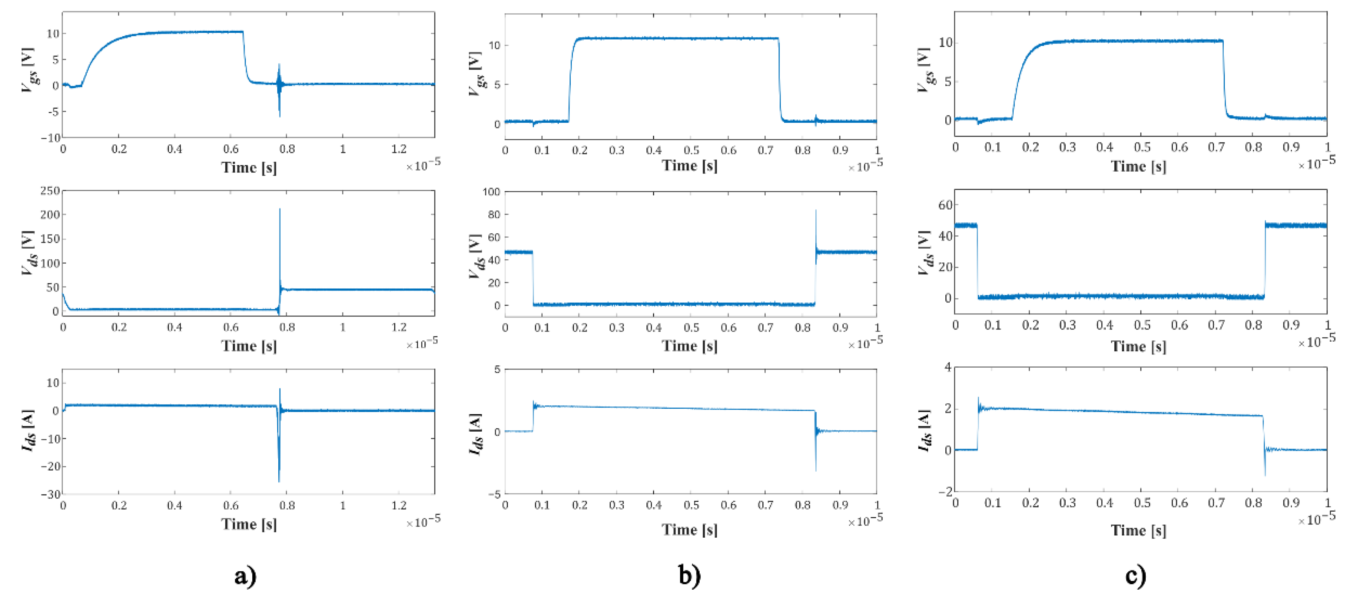
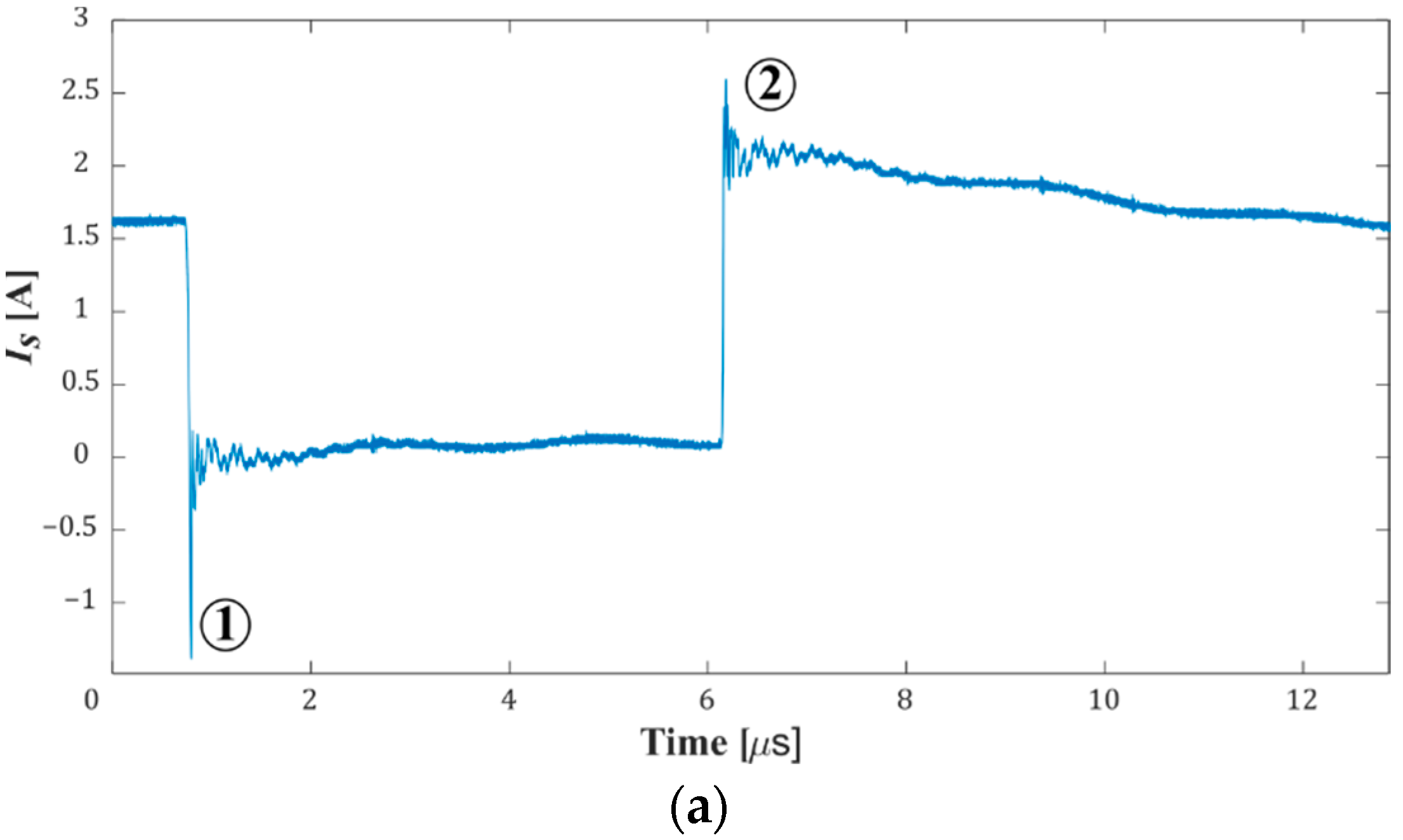
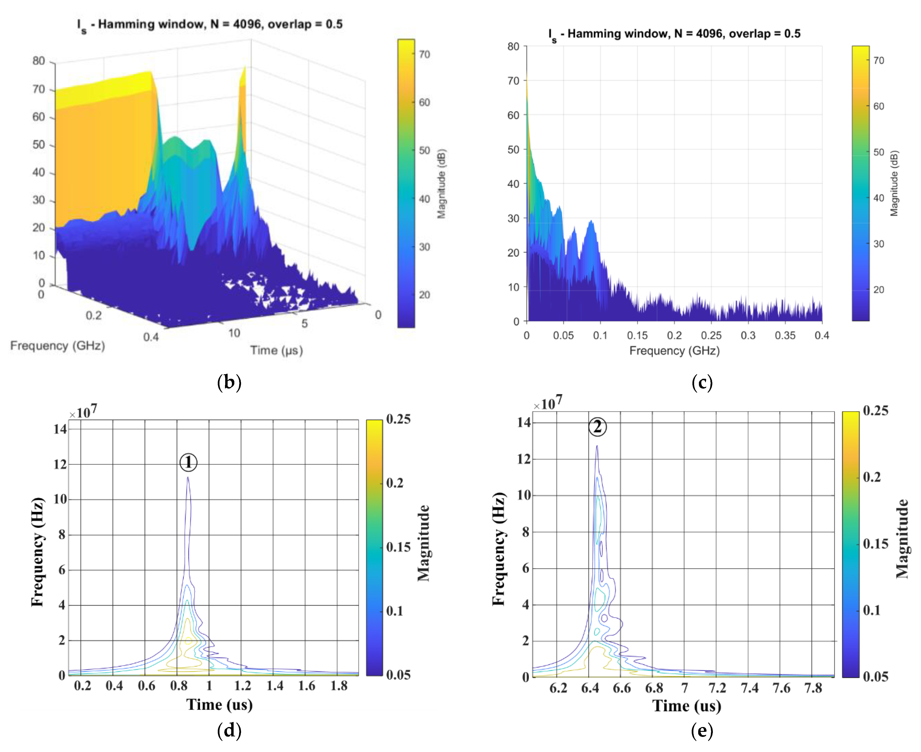
  • Case in which a false turn-on appears reflected in an overvoltage at Δ V ~ 160   V and an overcurrent Δ I = 27.5   A and Δ I = 8.4   A .
  • Switching case with gate resistor R g = 15   Ω , resulting in a higher overshoot in voltage and current Δ I = 0.3   A and Δ I = 3.2   A (due to reverse recovery current).
  • Switching case with gate resistor R g = 82   Ω , resulting in a current overshoot, Δ I = 0.7   A and Δ I = 1.3   A (due to reverse recovery current).
Similar parameter sensitivity tests were carried out with respect to source gate capacitance, radiator connection mode obtaining in the same way commutations with different characteristics of the overshoot level, and rise and fall time (in the magnitude order about ~ 10 40   ns , but they are considered redundant and are not shown here).

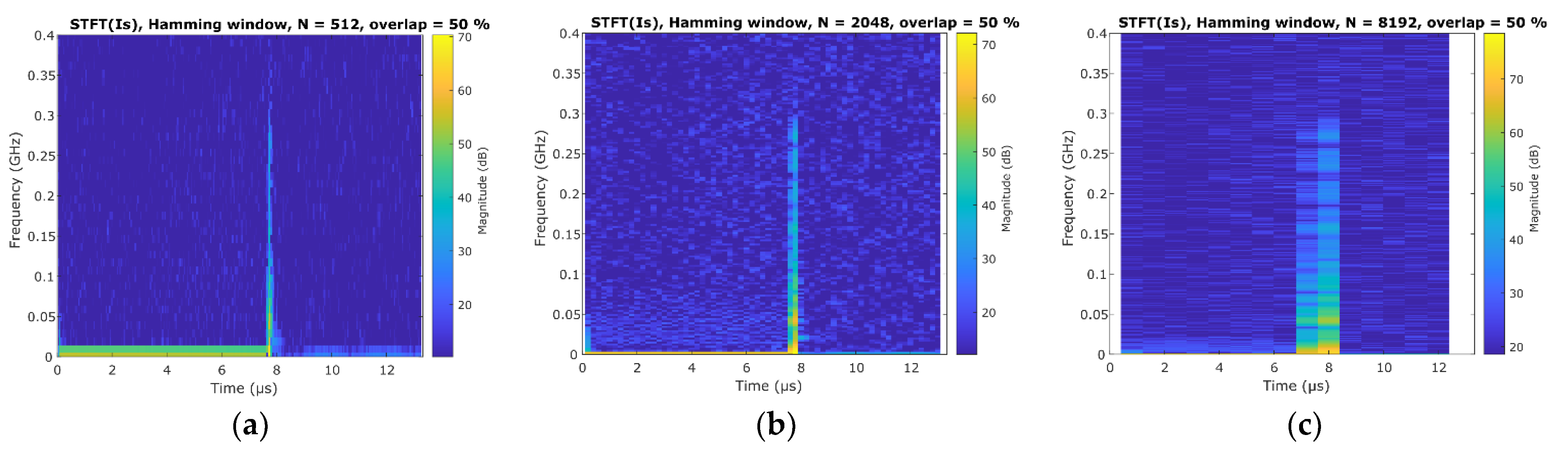
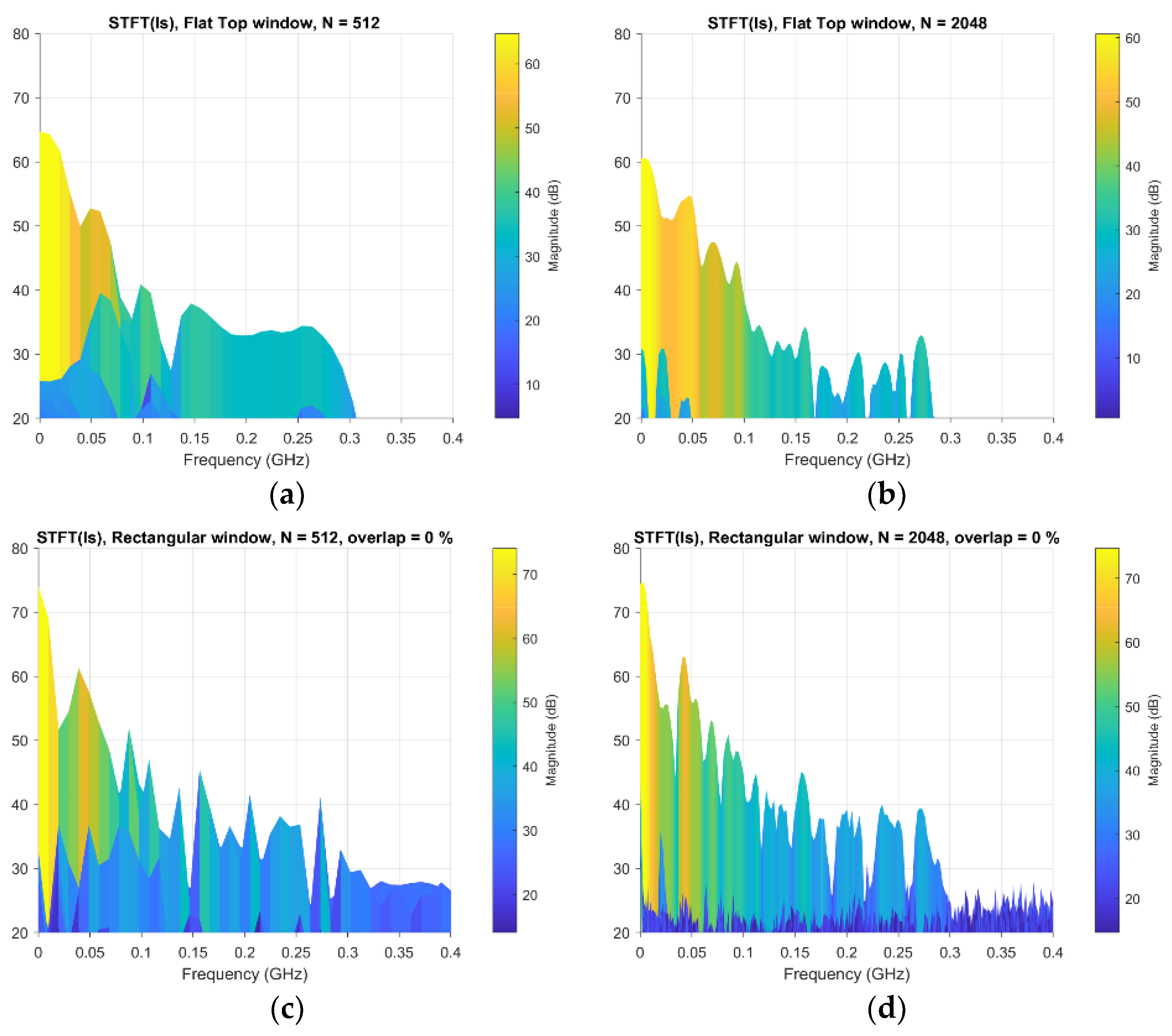
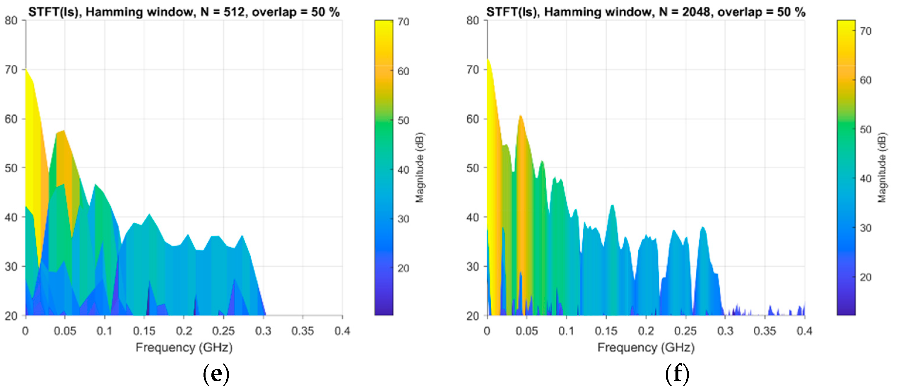
4.2. Spectrum Analysis Results

From the analysis presented in Section 2.2, the time signals of Section 4.1 were taken, and the spectral analysis using STFT and CWT was carried out in MATLAB. Some of the results of this analysis are shown in Figure 7, Figure 8 and Figure 9.
For STFT, several windows were tested, by varying the overlap and number of points in each one, to analyse both the time and frequency resolution. The aim was to see if the optimal values for the STFT configuration parameters can be determined, as the literature reports, for example, that STFT is very sensitive to window size and hop size [39].
First, Figure 7 shows the influence of the window length and number of points on the achieved time resolution. The results show a time range where the spectrum reaches higher frequencies, but the ability to discriminate the exact instant of switching goes from Δ t = 0.15   μ s to Δ t = 1.5   μ s as the window length increases from N = 512 to N = 8192 . As expected, this has an inverse effect in the frequency resolution, as using a smaller number of points does not allow the discrimination of closer frequency components. As with an RF receiver which depends on the bandwidth of the filters used, in this case not having sufficient spectral resolution results in masking possible discrete frequency peaks close to each other and considering them as a single component with a wider bandwidth.
Figure 8 shows the results corresponding to three different types of windows: (a) and (b) flat top windows (pros: minimal scalloping loss or reduction in the signal level in the frequency domain; drawbacks: poorer frequency resolution and high noise bandwidth); (c) and (d) rectangular windows (appropriate when analysing the transient of signals where the energy vs. time distribution is uneven); and (e) and (f) Hamming windows (with a sinusoidal shape that gives a wide peak and low side lobes). Analogous analyses were performed with other types of windows such as Blackman–Harris (similar to Hamming, the resulting spectrum has a wide peak but good side lobe compression), although the results are not shown here to avoid being redundant.
In each case, for each type of window, the overlap considered optimal [57,58,59] is shown. This parameter could be considered another factor to be taken into account when analysing the validity and feasibility of the STFT analysis, but it makes no sense to try to work with values outside those considered optimal.
As previously stated, the number of points used is key to the frequency resolution as well as to determine the frequency components of the ringing that occurs in the switching signals.
In the case of wavelet analysis, a CWT (continuous wavelet transform) was performed using different numbers of octaves and voices per octave for the selected wavelet types, as seen in Figure 9.
The difference between wavelet types lies in the ability to localise events in time and/or frequency, and the configuration of the characteristic parameters of each wavelet allows optimal results to be achieved.
In general, the number of octaves is decisive in determining the minimum frequency that will be detectable, given that the value of the maximum frequency is determined by the sampling period of the experimental signals. On the other hand, the number of voices per octave refers to the number of intermediate steps in each octave or, in other words, to the “finesse” or level of resolution with which the scaling is discretised (the greater the number of voices, the greater the “finesse” but the greater the computational load).
The wavelets used were Morlet, Morse and Bump, whose main characteristics were described extensively in [60].
The result of the analysis is similar in all cases but with some significant differences between the wavelet types. To begin with, as was evident, all wavelets are capable of locating in time the switching events and oscillations in which higher frequency components appear. (We have omitted to represent the complete period because it is considered to be of no interest.)
In terms of time and frequency resolution, the bump wavelet shows a lower temporal resolution but is more precise, delimiting the value of a resonant peak at 45 ± 2   MHz . However, it is not capable of detecting lower frequency peaks around 7 MHz, as the Morse and Morlet wavelets do.
The results reveal another aspect that is fundamental to understanding the origin of the emissions, namely, the possibility of discriminating whether the higher level of the envelope and the peaks that appear in the spectrum are fundamentally due to events that occur during the turning on or turning off of the transistors. Figure 10 shows an example of this characteristic, in this case, on the current flowing through the bottom transistor. Although at first glance there are oscillations at both the turn-on and turn-off, the spectrum associated with each is different. The three-dimensional image in Figure 10b corresponding to the STFT calculation shows this. This detail would be lost if we used the FFT, but through the wavelet transform in Figure 10d,e, the differences can be seen.
If we are able to associate in each case the resonant peaks to specific phenomena (ringing, reverse diode recovery current), this can help when implementing attenuation and cancellation measures.
In any case, the results show that on the envelope of the spectrum that would correspond to a trapezoidal-shaped switching wave, peaks clearly appear due to the oscillations produced in this time wave.

5. Conclusions and Future Work

The work carried out has provided an overview of the main temporal and frequency characteristics of the converter signals and has taken the first step in the development of a model for the noise generators and propagation paths.
The need for the accurate measurements of time signals and the influence that the selection of some elements, such as voltage and current test probes, was shown. Similarly, the need for adequate tools for spectral analysis was demonstrated. In this sense, it was shown that both the STFT and the wavelet transform can be suitable and complementary tools for obtaining the frequency characteristics of the switching signal.
The combination of precise measurements with measuring elements capable of detecting rapid signal variations and the use of the above-mentioned spectral analysis techniques allowed the detection of frequency components on the envelope and noise floor up to 300 MHz.
Not only that, but the possibility offered by these two temporal–frequency analysis techniques to discriminate the events produced in the switching on and off of transistors has also been demonstrated.
In this way, we can overcome one of the main gaps pointed out in the introduction, which is to be able to see and relate the temporal events and corresponding peaks in the spectrum through a complete experimental signal and not through a theoretical or partial decomposition of the signal, as it seemed to be performed in other references [26,27].
On the other hand, it cannot be established in a general way which is the optimal one for every type of signal, and a trade-off solution must be made between a time and frequency resolution.
The next step in this work will be to define the equivalent noise generators, differentiating between common-mode noise and differential-mode noise, based on the combination of the measured switching signals. The previous work by Bishnoi on behavioural models for EMI modelling or the more recent work by Brovont, Lemmon, Kolar and others will provide valuable starting points [6,11,12,16,17]. These, together with the determination of the characteristics of the propagation paths, will allow the development of a noise generation and propagation model that can simulate the conducted and radiated emission levels.
As noted in the introduction, the definition of the noise generators and the subsequent definition of the complete model, together with the propagation paths, can allow power electronics engineers to predict the frequency ranges in which their designs may generate higher levels of EMI noise in order to anticipate potential problems and design attenuation or cancellation measures by acting on those particular noise sources.

Author Contributions

Conceptualization, J.O. and I.A.; methodology, J.O. and I.A.; validation, J.O., I.A. and I.B.-E.; formal analysis, J.O.; investigation, J.O., I.A. and I.B.-E.; writing—original draft preparation, J.O.; writing—review and editing, I.A. and I.B.-E.; supervision, I.A. and I.B.-E.; project administration, J.O. and I.A. All authors have read and agreed to the published version of the manuscript.

Funding

This research received no external funding.

Institutional Review Board Statement

Not applicable.

Informed Consent Statement

Not applicable.

Data Availability Statement

Not applicable.

Conflicts of Interest

The authors declare no conflict of interest.

References

  1. Nagel, A.; De Doncker, R. Analytical approximations of interference spectra generated by power converters. In Proceedings of the IAS’97. Conference Record of the 1997 IEEE Industry Applications Conference Thirty-Second IAS Annual Meeting, New Orleans, LA, USA, 5–9 October 1997; Volume 2, pp. 1564–1570. [Google Scholar] [CrossRef]
  2. Zhu, H.; Lai, J.; Hefner, A.; Tang, Y.; Chen, C. Modeling-Based Examination of Conducted EMI Emissions from Hard- and Soft-Switching PWM Inverters. IEEE Trans. Ind. Appl. 2001, 37, 1383–1393. [Google Scholar] [CrossRef]
  3. Julian, A.; Oriti, G.; Lipo, T. Elimination of common-mode voltage in three-phase sinusoidal power converters. IEEE Trans. Power Electron. 1999, 14, 982–989. [Google Scholar] [CrossRef]
  4. Ogasawara, S.; Ayano, H.; Akagi, H. An active circuit for cancellation of common-mode voltage generated by a PWM inverter. IEEE Trans. Power Electron. 1998, 13, 835–841. [Google Scholar] [CrossRef] [Green Version]
  5. Rendusara, D.; Enjeti, P. An improved inverter output filter configuration reduces common and differential modes dv/dt at the motor terminals in PWM drive systems. IEEE Trans. Power Electron. 1998, 13, 1135–1143. [Google Scholar] [CrossRef]
  6. Lemmon, A.N.; Brovont, A.D.; New, C.D.; Nelson, B.W.; DeBoi, B.T. Modeling and Validation of Common-Mode Emissions in Wide Bandgap-Based Converter Structures. IEEE Trans. Power Electron. 2020, 35, 8034–8049. [Google Scholar] [CrossRef]
  7. Liu, T.; Ning, R.; Wong, T.T.Y.; Shen, Z.J. Modeling and Analysis of SiC MOSFET Switching Oscillations. IEEE J. Emerg. Sel. Top. Power Electron. 2016, 4, 747–756. [Google Scholar] [CrossRef]
  8. Wu, Y.; Li, H.; Li, C.; Bi, C.; Zhi, Y.; Yao, W.; Liu, G. Analytical Modeling of SiC MOSFET during Switching Transient. In Proceedings of the 2018 IEEE International Symposium on Electromagnetic Compatibility and 2018 IEEE Asia-Pacific Symposium on Electromagnetic Compatibility (EMC/APEMC), Suntec City, Singapore, 14–18 May 2018; pp. 1187–1192. [Google Scholar] [CrossRef]
  9. Liang, M.; Zheng, T.Q.; Li, Y. An Improved analytical model for predicting the switching performance of SiC MOSFETs. J. Power Electron. 2016, 16, 374–387. [Google Scholar] [CrossRef] [Green Version]
  10. Ahmed, M.R.; Todd, R.; Forsyth, A.J. Analysis of SiC MOSFETs under hard and soft-switching. In Proceedings of the 2015 IEEE Energy Conversion Congress and Exposition ECCE, Montreal, QC, Canada, 20–24 September 2015; pp. 2231–2238. [Google Scholar] [CrossRef]
  11. Heller, M.J.; Krismer, F.; Kolar, J.W. EMI Filter Design for the Integrated Dual Three-Phase Active Bridge (D3AB) PFC Rectifier. IEEE Trans. Power Electron. 2022, 37, 14527–14546. [Google Scholar] [CrossRef]
  12. Niklaus, P.S.; Antivachis, M.M.; Bortis, D.; Kolar, J.W. Analysis of the influence of measurement circuit asymmetries on three-phase CM/DM conducted EMI separation. IEEE Trans. Power Electron. 2020, 36, 4066–4080. [Google Scholar] [CrossRef]
  13. Papamanolis, P.; Bortis, D.; Krismer, F.; Menzi, D.; Kolar, J.W. New EV battery charger PFC rectifier front-end allowing full power delivery in 3-phase and 1-phase operation. Electronics 2021, 10, 2069. [Google Scholar] [CrossRef]
  14. Menzi, D.; Bortis, D.; Kolar, J.W. EMI Filter Design for a Three-Phase Buck–Boost Y-Inverter VSD with Unshielded Motor Cables Considering IEC 61800-3 Conducted and Radiated Emission Limits. IEEE Trans. Power Electron. 2021, 36, 12919–12937. [Google Scholar] [CrossRef]
  15. Antivachis, M.; Zurich, E. Input/Output EMI Filter Design for Three-Phase Ultra-High Speed Motor Drive GaN Inverter Stage. CPSS Trans. Power Electron. Appl. 2021, 6, 74–92. [Google Scholar] [CrossRef]
  16. Bishnoi, H.; Mattavelli, P.; Burgos, R.; Boroyevich, D. EMI Behavioral Models of DC-Fed Three-Phase Motor Drive Systems. IEEE Trans. Power Electron. 2013, 29, 4633–4645. [Google Scholar] [CrossRef]
  17. Bishnoi, H. Behavioral EMI Models of Switched Power Converters Behavioral EMI Models of Switched Power Converters. Doctoral Dissertation, Virginia Polytechnic Institute and State University, Blacksburg, VA, USA, 2013. [Google Scholar]
  18. Sun, B.; Burgos, R.; Boroyevich, D. Common-Mode EMI Unterminated Behavioral Model of Wide-Bandgap-Based Power Converters Operating at High Switching Frequency. IEEE J. Emerg. Sel. Top. Power Electron. 2018, 7, 2561–2570. [Google Scholar] [CrossRef]
  19. Brovont, A.D.; Pekarek, S.D. Derivation and Application of Equivalent Circuits to Model Common-Mode Current in Microgrids. IEEE J. Emerg. Sel. Top. Power Electron. 2016, 5, 297–308. [Google Scholar] [CrossRef]
  20. Liu, Q.; Wang, F.; Boroyevich, D. Modular-terminal-behavioral (MTB) model for characterizing switching module conducted EMI generation in converter systems. IEEE Trans. Power Electron. 2006, 21, 1804–1814. [Google Scholar] [CrossRef]
  21. Sun, B.; Burgos, R.; Zhang, X.; Boroyevich, D. Differential-mode EMI emission prediction of SiC-based power converters using a mixed-mode unterminated behavioral model. In Proceedings of the 2015 IEEE Energy Conversion Congress and Exposition, ECCE, Montreal, QC, Canada, 20–24 September 2015; pp. 4367–4374. [Google Scholar] [CrossRef]
  22. Karaca, T.; Deutschmann, B.; Winkler, G. EMI-receiver simulation model with quasi-peak detector. In Proceedings of the IEEE International Symposium on Electromagnetic Compatibility, Montreal, QC, Canada, 20–24 September 2015; pp. 891–896. [Google Scholar] [CrossRef]
  23. Gómez-Luna, E.; Mayor, G.A.; Guerra, J.P.; Salcedo, D.F.S.; Gutierrez, D.H. Application of Wavelet Transform to Obtain the Frequency Response of a Transformer From Transient Signals—Part 1: Theoretical Analysis. IEEE Trans. Power Deliv. 2013, 28, 1709–1714. [Google Scholar] [CrossRef]
  24. Kachhepati, B. Application of Short Time Fourier Transform (STFT) in Power Quality Monitoring and Event Classification. Doctoral Dissertation, New Mexico State Universiry, Las Cruces, NM, USA, 2016. [Google Scholar]
  25. Alam, A.; Mukul, M.K.; Thakura, P. Wavelet Transform-Based EMI Noise Mitigation in Power Converter Topologies. IEEE Trans. Electromagn. Compat. 2016, 58, 1662–1673. [Google Scholar] [CrossRef]
  26. Zhang, B.; Wang, S. A Survey of EMI Research in Power Electronics Systems With Wide-Bandgap Semiconductor Devices. IEEE J. Emerg. Sel. Top. Power Electron. 2019, 8, 626–643. [Google Scholar] [CrossRef]
  27. Zhang, Y.; Wang, S.; Chu, Y. Analysis and Comparison of the Radiated Electromagnetic Interference Generated by Power Converters with Si MOSFETs and GaN HEMTs. IEEE Trans. Power Electron. 2020, 35, 8050–8062. [Google Scholar] [CrossRef]
  28. Wang, J.; Chung, H.S.-H.; Li, R.T.-H. Characterization and Experimental Assessment of the Effects of Parasitic Elements on the MOSFET Switching Performance. IEEE Trans. Power Electron. 2012, 28, 573–590. [Google Scholar] [CrossRef]
  29. Roscoe, N.M.; Holliday, D.; McNeill, N.; Finney, S.J. LV Converters: Improving Efficiency and EMI Using Si MOSFET MMC and Experimentally Exploring Slowed Switching. IEEE J. Emerg. Sel. Top. Power Electron. 2018, 6, 2159–2172. [Google Scholar] [CrossRef] [Green Version]
  30. Chen, Z. Characterization and Modeling of High-Switching-Speed Behavior of SiC Active Devices. Doctoral Dissertation, Virginia Tech, Blacksburg, VA, USA, 2009. [Google Scholar]
  31. Chen, Z.; Boroyevich, D.; Burgos, R. Experimental parametric study of the parasitic inductance influence on MOSFET switching characteristics. In Proceedings of the 2010 International Power Electronics Conference, Sapporo, Japan, 21–24 June 2010; pp. 1–6. [Google Scholar] [CrossRef]
  32. Jin, M.; Weiming, M. Power Converter EMI Analysis Including IGBT Nonlinear Switching Transient Model. IEEE Trans. Ind. Electron. 2006, 53, 1577–1583. [Google Scholar] [CrossRef]
  33. Beghou, L.; Costa, F.; Pichon, L. Detection of Electromagnetic Radiations Sources at the Switching Time Scale Using an Inverse Problem-Based Resolution Method—Application to Power Electronic Circuits. IEEE Trans. Electromagn. Compat. 2014, 57, 52–60. [Google Scholar] [CrossRef]
  34. Oswald, N.; Anthony, P.; McNeill, N.; Stark, B.H. An Experimental Investigation of the Tradeoff between Switching Losses and EMI Generation With Hard-Switched All-Si, Si-SiC, and All-SiC Device Combinations. IEEE Trans. Power Electron. 2013, 29, 2393–2407. [Google Scholar] [CrossRef]
  35. Zaman, H.; Wu, X.; Zheng, X.; Khan, S.; Ali, H. Suppression of Switching Crosstalk and Voltage Oscillations in a SiC MOSFET Based Half-Bridge Converter. Energies 2018, 11, 3111. [Google Scholar] [CrossRef] [Green Version]
  36. Costa, F.; Vollaire, C.; Meuret, R. Graphical Analysis of the Spectra of EMI Sources in Power Electronics. IEEE Trans. Electromagn. Compat. 2005, 20, 1491–1498. [Google Scholar] [CrossRef]
  37. Middelstaedt, L.; Lindemann, A.; Al-Hamid, M.; Vick, R. Influence of parasitic elements on radiated emissions of a boost converter. In Proceedings of the IEEE International Symposium on Electromagnetic Compatibility, Dresden, Germany, 16–22 August 2015; pp. 755–760. [Google Scholar] [CrossRef]
  38. Middelstaedt, L.; Lindemann, A. Methodology for analysing radiated EMI characteristics using transient time domain measurements. IET Power Electron. 2016, 9, 2013–2018. [Google Scholar] [CrossRef]
  39. Ashouri, M.; Silva, F.F.; Bak, C.L. Application of short-time Fourier transform for harmonic-based protection of meshed VSC-MTDC grids. J. Eng. 2018, 2019, 1439–1443. [Google Scholar] [CrossRef]
  40. Delgado, A.M.S. Electric-Device Characterization for Interference Prediction and Mitigation by an Optimal Filtering Design. Doctoral Dissertation, Universitat Ramon LLull, Barcelona, Spain, 2010. [Google Scholar]
  41. Sandrolini, L.; Mariscotti, A. Impact of short-time fourier transform parameters on the accuracy of EMI spectra estimates in the 2–150 kHz supraharmonic interval. Electr. Power Syst. Res. 2021, 195, 107130. [Google Scholar] [CrossRef]
  42. Bozhokin, S.V.; Sokolov, I.M. Comparison of the Wavelet and Gabor Transforms in the Spectral Analysis of Nonstationary Signals. Tech. Phys. 2018, 63, 1711–1717. [Google Scholar] [CrossRef]
  43. Zhao, C.; He, M.; Zhao, X. Analysis of transient waveform based on combined short time Fourier transform and wavelet transform. In Proceedings of the 2004 International Conference on Power System Technology, Singapore, 21–24 November 2004; pp. 1122–1126. [Google Scholar] [CrossRef]
  44. Jurado, F.; Saenz, R. Comparison between discrete STFT and wavelets for the analysis of power quality events. Electr. Power Syst. Res. 2002, 62, 183–190. [Google Scholar] [CrossRef]
  45. Grcić, D.; Pandžić, I.; Novosel, H. Fault detection in dc microgrids using short-time fourier transform. Energies 2021, 14, 277. [Google Scholar] [CrossRef]
  46. Genc, S.; Gundogdu, B.M.; Ozgonenel, O. Conducted Emissions Analysis of DC-DC Buck Converter. In Proceedings of the 2022 4th Global Power, Energy and Communication Conference (GPECOM), Nevsehir, Turkey, 14–17 June 2022; pp. 135–138. [Google Scholar] [CrossRef]
  47. Rajoub, B. Characterization of Biomedical Signals: Feature Engineering and Extraction; Elsevier Inc.: Amsterdam, The Netherlands, 2020. [Google Scholar]
  48. Sanchez, J.G.; Isaac, I.; Agudelo, H.C.; Díez, A.; Jiménez, D.; Jiménez, G.L. Aplicación de la transformada de wavelet para el análisis de transitorios debidos a la conmutación de bancos de condensadores. Investig. Apl. 2010, 4, 33–45. [Google Scholar]
  49. McGrew, T.; Sysoeva, V.; Cheng, C.-H.; Miller, C.; Scofield, J.; Scott, M.J. Condition Monitoring of DC-Link Capacitors Using Time–Frequency Analysis and Machine Learning Classification of Conducted EMI. IEEE Trans. Power Electron. 2022, 37, 12606–12618. [Google Scholar] [CrossRef]
  50. Fedotenkova, M.; Hutt, A. Comparison of Different Time-Frequency Representations. Doctoral Dissertation, INRIA Nancy, Villers-lès-Nancy, France, 2014. [Google Scholar]
  51. Zhang, Z.; Guo, B.; Wang, F.F.; Jones, E.A.; Tolbert, L.M.; Blalock, B.J. Methodology for Wide Band-Gap Device Dynamic Characterization. IEEE Trans. Power Electron. 2017, 32, 9307–9318. [Google Scholar] [CrossRef]
  52. Garrido, D.; Baraia-Etxaburu, I.; Arza, J.; Barrenetxea, M. Simple and Affordable Method for Fast Transient Measurements of SiC Devices. IEEE Trans. Power Electron. 2019, 35, 2933–2942. [Google Scholar] [CrossRef]
  53. Li, H.; Beczkowski, S.; Munk-Nielsen, S.; Lu, K.; Wu, Q. Current measurement method for characterization of fast switching power semiconductors with Silicon Steel Current Transformer. In Proceedings of the Conference Proceedings—IEEE Applied Power Electronics Conference and Exposition—APEC, Charlotte, NC, USA, 15–19 March 2015; pp. 2527–2531. [Google Scholar] [CrossRef]
  54. Ardizzoni, B.J. High-Speed Time-Domain Measurements—Practical Tips for Improvement. Analog. Dialogue 2007, 41, 13–18. [Google Scholar]
  55. New, C.; Lemmon, A.N.; Shahabi, A. Comparison of methods for current measurement in WBG systems. In Proceedings of the 2017 IEEE 5th Workshop on Wide Bandgap Power Devices and Applications, WiPDA 2017, Albuquerque, NM, USA, 30 October–1 November 2017; pp. 87–92. [Google Scholar] [CrossRef]
  56. Shelton, E.; Hari, N.; Zhang, X.; Zhang, T.; Zhang, J.; Palmer, P. Design and measurement considerations for WBG switching circuits. In Proceedings of the 2017 19th European Conference on Power Electronics and Applications, EPE’17 ECCE Europe, Warsaw, Poland, 11–14 September 2017. [Google Scholar] [CrossRef]
  57. Heinzel, G.; Rudiger, A.; Schilling, R. Spectrum and spectral density estimation by the Discrete Fourier transform (DFT), including a comprehensive list of window functions and some new flat-top windows. 2002. [Google Scholar]
  58. Prabhu, K.M. Window Functions and Their Applications in Signal Processing; Taylor & Francis Group: Abingdon, UK, 2014. [Google Scholar]
  59. Selvi, R.S.; Kumar, P.S.; Krishna, R.S.; Rao, S.S. Speech Enhancement using Adaptive Filtering with Different Window Functions and Overlapping Sizes Turkish Journal of Computer and Mathematics Education Research Article. Turk. J. Comput. Math. Educ. 2021, 12, 1886–1894. [Google Scholar]
  60. Silik, A.; Noori, M.; Altabey, W.A.; Ghiasi, R.; Wu, Z. Comparative Analysis of Wavelet Transform for Time-Frequency Analysis and Transient Localization in Structural Health Monitoring. Struct. Durab. Health Monit. 2021, 15, 1–22. [Google Scholar] [CrossRef]
Figure 1. Block diagram of a switching system, noise sources and propagation paths for common mode (CM) and differential mode (DM), and EMI measurement.
Electronics 11 03898 g001
Figure 2. Basic current and voltage switching waves’ time domain characteristics.
Electronics 11 03898 g002
Figure 3. Spectrum and envelope of a basic trapezoidal switching wave and effect of changing parameters such as switching frequency, d v / d t or d i / d t . In red, appearance of peaks on the envelope due to ringing effects.
Electronics 11 03898 g003
Figure 4. Test bench for measurement of switching waveforms: (a) block diagram of a half-bridge and positioning of measuring probes; (b) PCB detail with location of current shunt and voltage probes.
Electronics 11 03898 g004
Figure 5. Detail of coaxial shunt: (a) with shortened pads (top) to reduce inductance, and original (bottom) with long 1” pads; (b) frequency response of reactance of current shunt resistor up to 30 MHz for original sensor (brown line) and shortened pads sensor (blue line).
Electronics 11 03898 g005
Figure 6. Results of experimental measurements for 3 different cases: (a) false turn-on; (b) switching with gate resistor R g = 15   Ω ; (c) switching with gate resistor R g = 82   Ω .
Electronics 11 03898 g006
Figure 7. Time resolution vs. frequency resolution in STFT calculation for different length Hamming windows: (a) N = 512 ; (b) N = 2048 ; (c) N = 8192 .
Electronics 11 03898 g007
Figure 8. STFT analysis comparison for several windows and window lengths: (a) flat top window N = 512 ; (b) flat top window N = 2048 ; (c) rectangular window N = 512 ; (d) rectangular window N = 2048 ; (e) Hamming window N = 512 ; (f) Hamming window N = 2048 .
Electronics 11 03898 g008aElectronics 11 03898 g008b
Figure 9. Wavelet analysis comparison using different wavelet types, number of octaves ( N o ) and number of voices ( N v ): (a) Morse wavelet N o = 13 , N v = 6 ; (b) Morse wavelet N o = 13 , N v = 40 ; (c) Morlet wavelet N o = 13 , N v = 6 ; (d) Morlet wavelet N o = 13 , N v = 40 ; (e) bump wavelet N o = 11 , N v = 6 ; (f) bump wavelet N o = 11 , N v = 40 .
Electronics 11 03898 g009
Figure 10. Event detection and discrimination using STFT and wavelet: (a) time signal I_s; (b) time–frequency–magnitude representation of the STFT; (c) frequency–magnitude representation of the STFT; (d) detail of the wavelet transform in the interval 0–2 μs using Morse wavelet; (e) detail of the wavelet transform in the interval 6–8 μs using Morse wavelet.
Electronics 11 03898 g010aElectronics 11 03898 g010b
Table 1. Summary of measuring probes characteristics.
TypeAdvantagesDrawbacks
Voltage probeDifferentialGalvanic isolationLow bandwidth
Connection leads
Voltage dividerVery high bandwidthLoading requirements
Not for V d s measurement
PassiveHigh bandwidth
Suitable for bridge low side measurement
Connection leads
Nongalvanic isolation
Current probeRogowski coilGalvanic isolation
Size
Low bandwidth (tenths of MHz)
Low accuracy
Current transformerGalvanic isolationLow bandwidth (up to ~100 MHz)
Added loop inductance
Larger size
Coaxial shuntHigh bandwidth (up to GHz)
High accuracy
AC-DC
Size
Non galvanic isolation
Added loop inductance
Heating
Publisher’s Note: MDPI stays neutral with regard to jurisdictional claims in published maps and institutional affiliations.

