Article

Investigation of Charge Transport Properties in VTP: PC71BM Organic Schottky Diode

by
Nur Adilah Roslan
1,2,*,
Azzuliani Supangat
2 and
Suresh Sagadevan
3,*
1
Department of Physics, Faculty of Science, Universiti Putra Malaysia, Serdang 43400, Selangor, Malaysia
2
Low Dimensional Materials Research Centre, Department of Physics, Faculty of Science, University of Malaya, Kuala Lumpur 50603, Malaysia
3
Nanotechnology & Catalysis Research Centre, University of Malaya, Kuala Lumpur 50603, Malaysia
*
Authors to whom correspondence should be addressed.
Electronics 2022, 11(22), 3777; https://doi.org/10.3390/electronics11223777
Submission received: 7 October 2022 / Revised: 31 October 2022 / Accepted: 14 November 2022 / Published: 17 November 2022
(This article belongs to the Special Issue Quantum and Optoelectronic Devices, Circuits and Systems)

Abstract

:
In this work, the charge transport properties of organic vanadyl 3,10,17,24-tetra-tert-butyl-1,8,15,22-tetrakis(dimethylamino)-29H,31H phthalocyanine (VTP) were investigated. The I-V profile demonstrated by single VTP shows a rectifying behavior, and Schottky diode parameters such as the ideality factor, barrier height, shunt, and series resistance were calculated. Further, the charge transport behavior of single-layer VTP and its blend with phenyl C71 butyric acid methyl ester (PC71BM) was evaluated using the I-V conventional method and diode analysis. In addition, the optimized diode properties of VTP: PC71BM were chosen to evaluate its photovoltaic effect. The current density-voltage (J-V) characteristics were evaluated in both dark and light conditions to determine the key parameters of the photovoltaic effect. The results indicate the optimized VTP: the PC71BM composite blend yielded a relatively low photovoltaic efficiency. However, due to the presence of extended ligands, it gives a very good sensitivity when applied in the organic photodetector device, as reported in our previous work.

1. Introduction

Organic electronic devices have gradually made their way into the commercial market to replace conventional inorganic electronic devices. The desire to improve the performance of organic semiconductor materials has prompted many researchers to look for new materials. Metal phthalocyanines (MPcs), in particular, have sparked considerable interest due to their enticing benefits, which include cost efficiency, eco-friendly organic material, and thermal and chemical stability. Organic materials have been widely evaluated in recent decades to overcome several shortcomings of their inorganic counterparts in optoelectronic applications. Some unique properties of organic materials, such as an enhanced sensitivity, cost-effectiveness, environmental friendliness, and the suitability of simple fabrication methods such as spin coating, drop casting, dip coating, and spray coating directly from liquid solutions, are advantageous for the fabrication of organic photovoltaics (OPVs) [1,2]. Over the years, bulk heterojunction (BHJ) OPV and organic photodiodes (OPDs) have been extensively researched, in which an acceptor and a donor are blended in the photoactive medium to develop a donor/acceptor (D/A) interface at the molecular level [3,4,5]. MPcs containing heterocyclic macrocyclic organic compounds have been thoroughly evaluated for many applications [6,7]. Several MPcs, including VOPcPhO [8,9,10,11,12,13], were used to evaluate OPVs and OPDs [8,9,10,11].
Organic devices such as organic field effect transistors (OFET) and organic photovoltaics (OPVs) can lead to the next level of advancement by using a fundamental device such as a metal/organic/metal-based Schottky diode [14]. One electrode in a Schottky diode is Ohmic (injecting), and the other is blocking [14]. The slope and intercept of the J-V characteristic in the linear and saturation regions can be used to calculate the ideality factor and carrier mobility, respectively [14]. A Schottky diode is a metal-semiconductor that is in contact with rectification properties, similar to a p-n junction diode [15]. A Schottky diode is a majority carrier device, as it has a fast switching speed [15]. In theory, both p-type and n-type semiconductors can be used to fabricate Schottky diodes from a wide range of semiconducting materials, including organic semiconductors [15]. To make a Schottky contact with semiconductors, metals such as Pd, Pt, Au, Ti, Al, W, Cr, molybdenum, and a few metal silicides, are used [15]. Various Schottky diode configurations have previously been studied, fabricated, and tested [16,17].
In this study, a vanadium metal complex MPc, known as VTP, is proposed. With the exception of its different extended ligands, the aromatic structure of VTP is similar to that of VOPcPhO. Essentially, the ligands in VTP have the potential to change the molecule’s photoabsorption sensitivity [18,19]. VTP has yet to be used as the active layer in the fabrication of OPVs. Based on the combination of their absorption properties, this study incorporated a blend of two organic compounds; a network structure is bound to improve charge separation and photogenerated charge carrier transport [20]. VTP is introduced as a donor material with distinct absorption properties, especially in the lower visible region [21]. The VTP and PC71BM have relatively exceptional hole-transport and electron-transport abilities, respectively [22], making them highly sought donor and acceptor components. The absorption of both materials plays an important role in capturing specific light wavelengths within the visible range. Light absorbance in the lower wavelength region of the visible spectrum is expected to increase due to the synergic absorption profile of the VTP and PC71BM matrix. Earlier, we reported a composite blend of VTP:PC71BM as an organic photodetector (OPD). The electrical characteristics of the OPD demonstrated improved sensing performances, and this could be attributed to the judicious selection of donor and acceptor components, which represented VTP and PC71BM, respectively [19]. Therefore, in this study, the VTP: PC71BM composites were utilized to study the charge transport properties and to investigate the photovoltaic effect of the composite blend.

2. Experimental Section

VTP and PC71BM were purchased from Sigma Aldrich (St. Louis, MO, USA) and used without modification. Each material was separately dissolved in chloroform to produce a 10 mg/mL solution, which was then continuously stirred for hours. VTP and PC71BM were mixed in three different volume ratios (1.0:1.0, 1.0:1.2, and 1.0:1.4), then stirred in a nitrogen-filled glove box for an hour. The experimental approach was briefly discussed in our earlier publication [19].

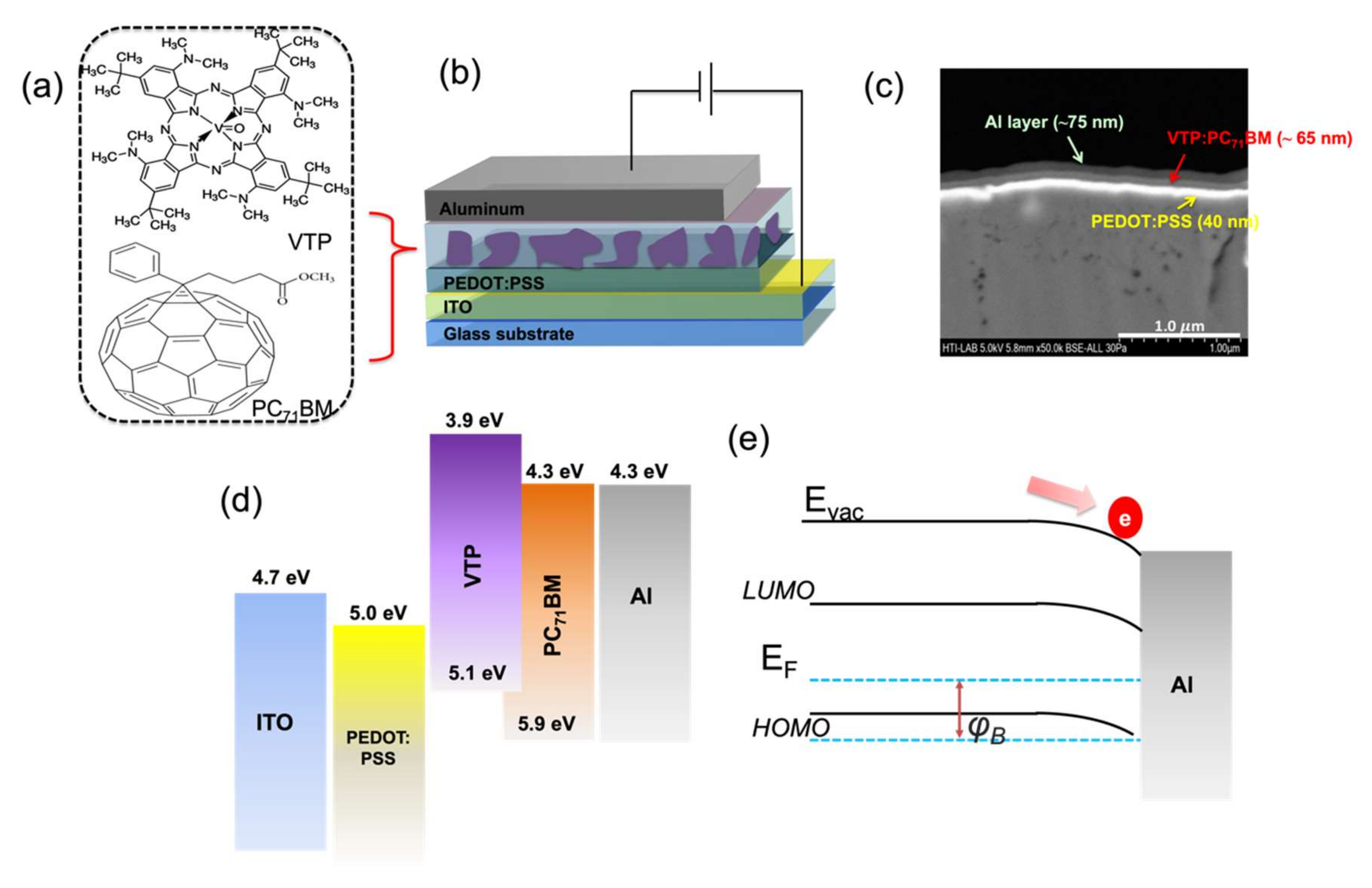
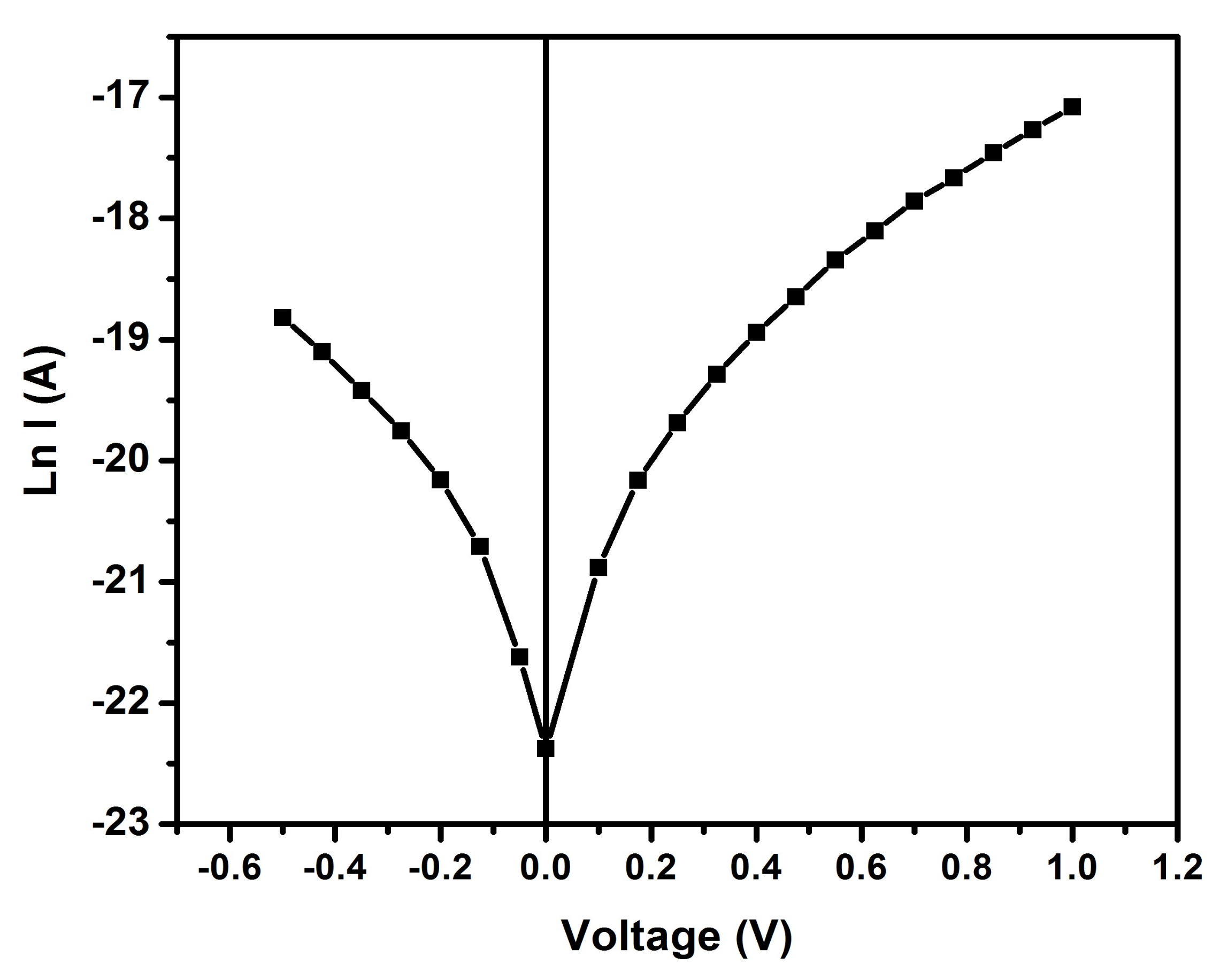
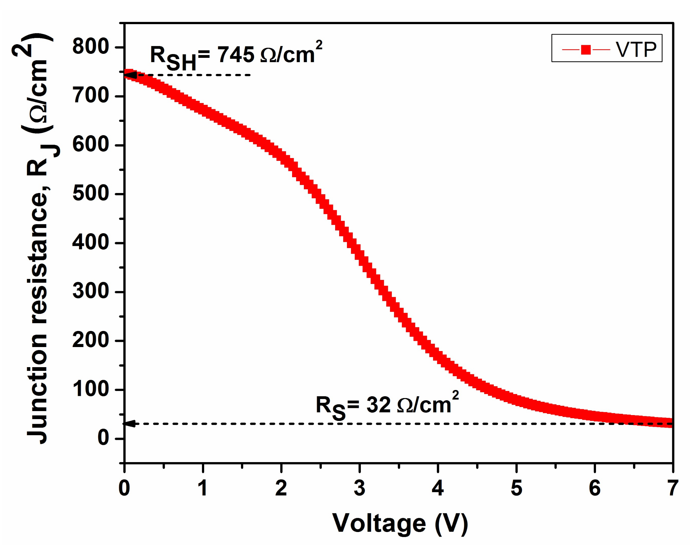
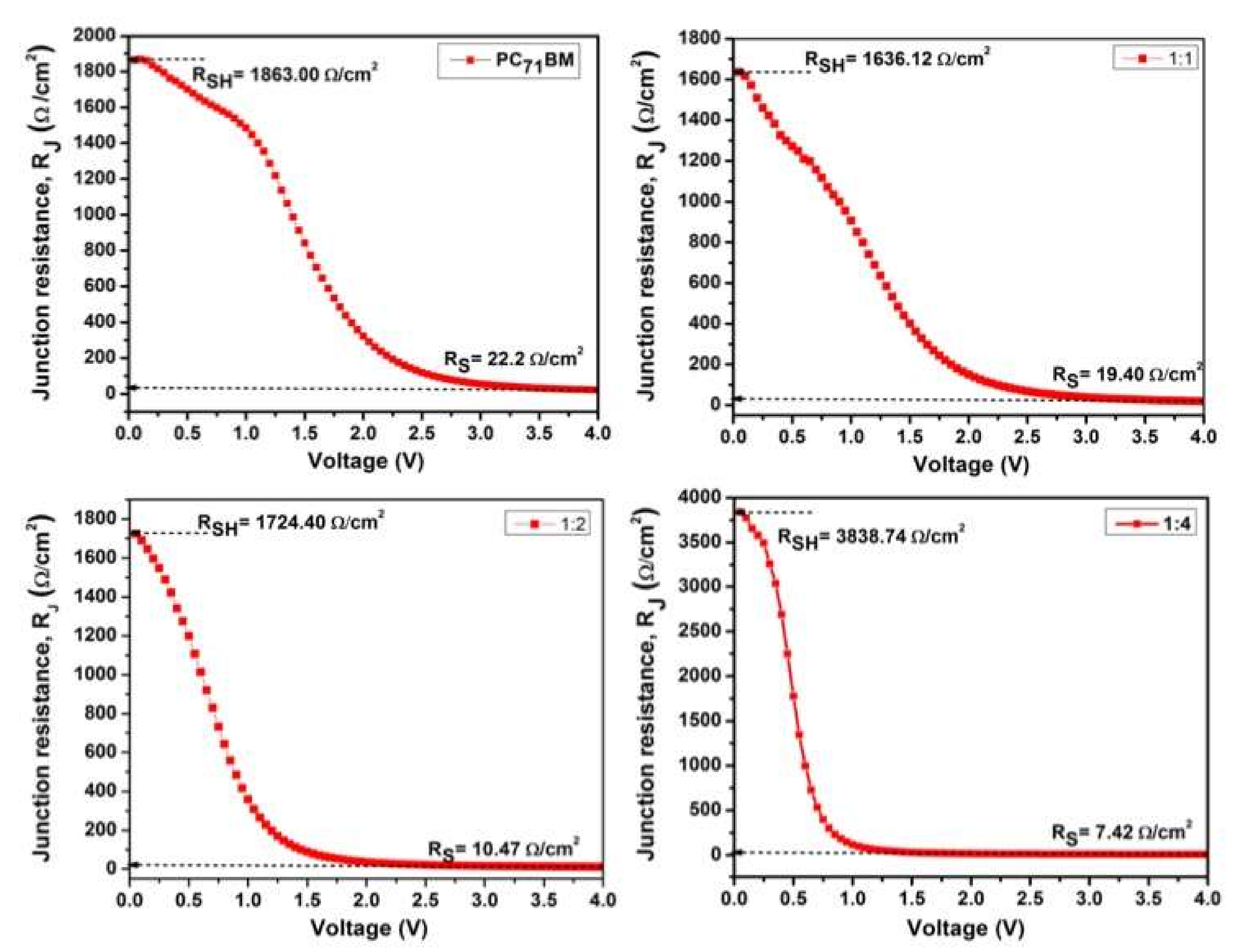
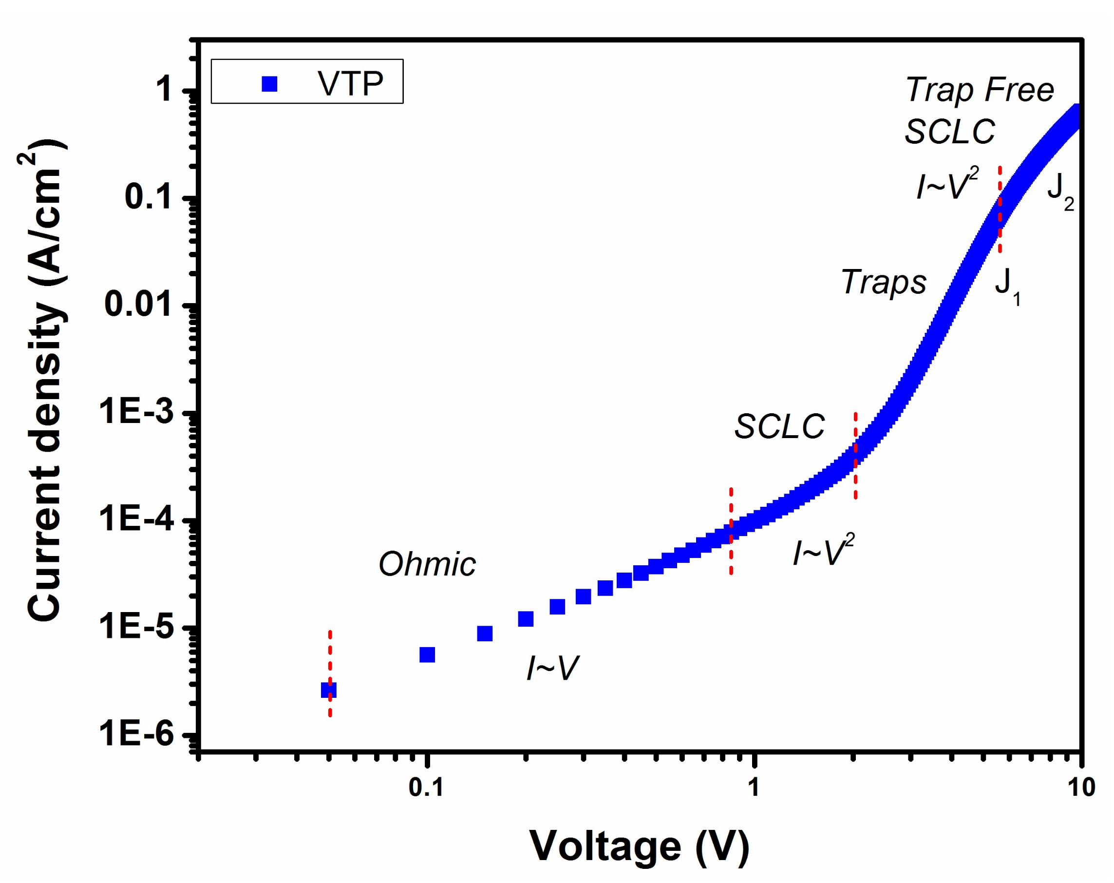
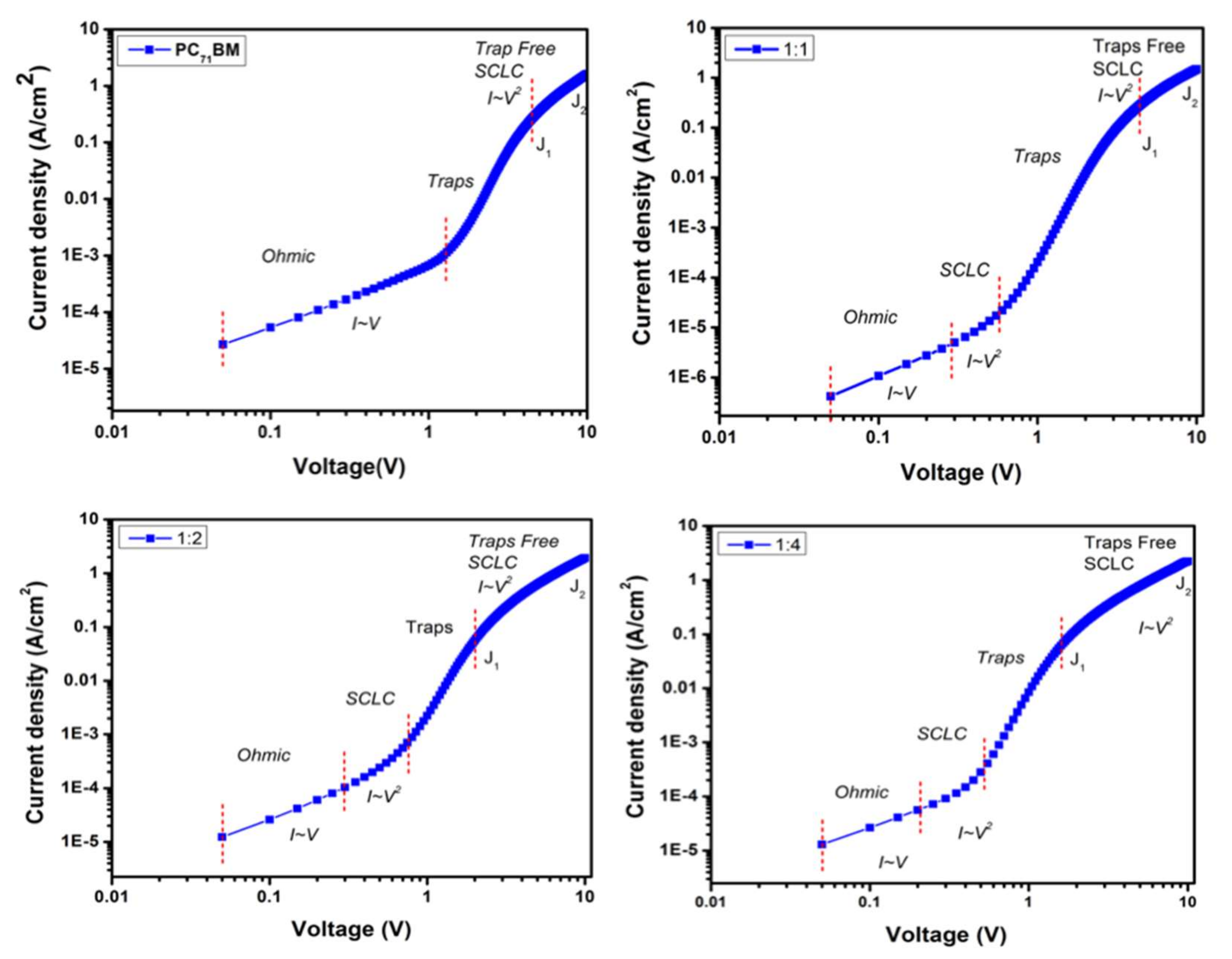
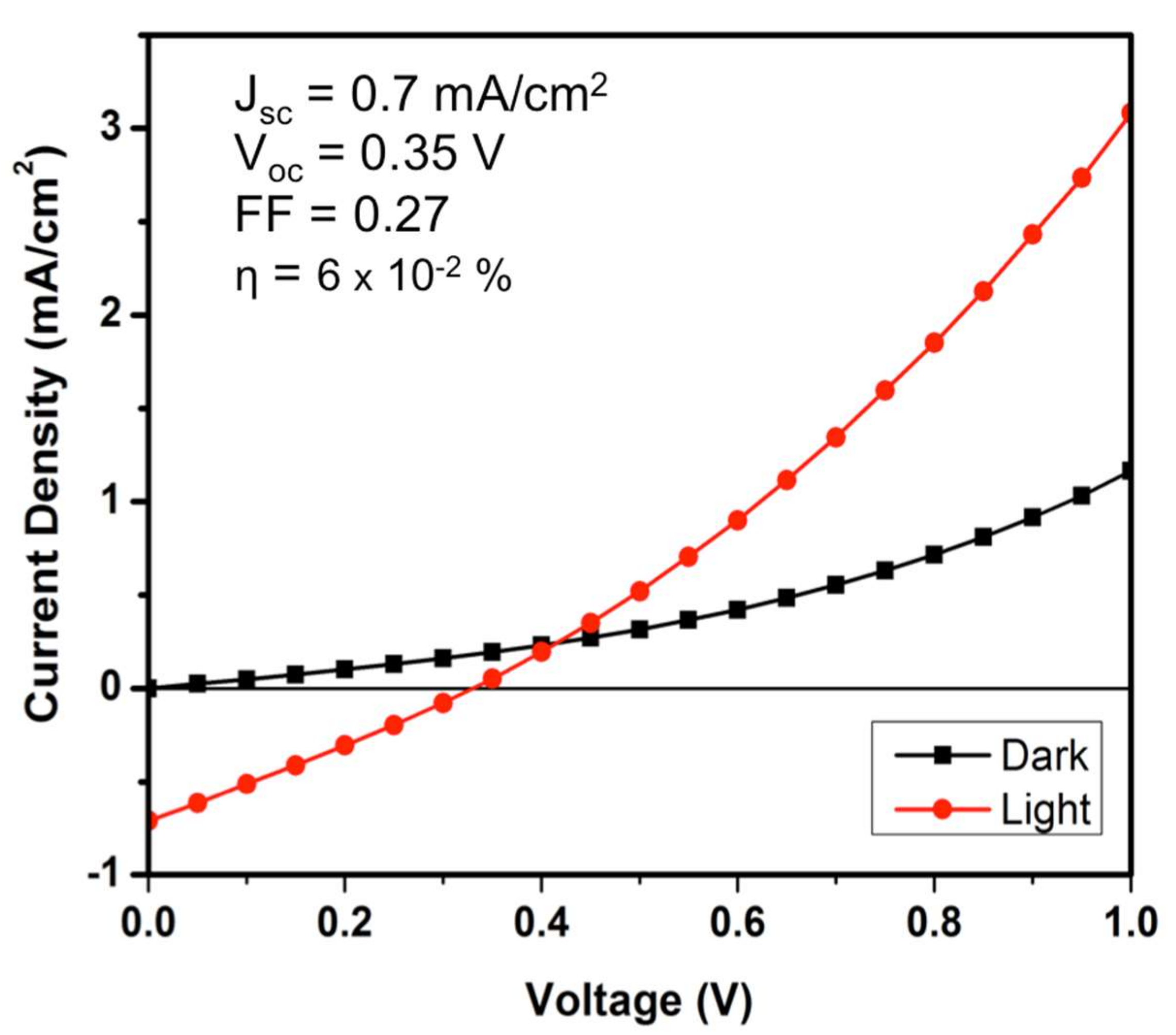
3. Results and Discussion

Figure 1 depicts (a) the molecular structure of VTP and PC71BM, (b) the schematic diagram of OPVs and OPDs, (c) a cross-section Field Effect Scanning Electron Microscopy (FESEM) image of the prepared samples, (d) the energy level diagram reported previously and (e) schematic diagram of energy levels for Schottky diode [19,23]. According to Figure 1c, the thicknesses of the PEDOT: PSS, active layer (VTP: PC71BM), and aluminum (Al) were 40, 65, and 75 nm, respectively.
The measurement of current-voltage (I-V) characteristics in a dark setting is extremely useful for evaluating junction properties. This analysis produced significant parameters such as the ideality factor, rectification ratio (RR), reverse saturation current, barrier height, shunt and series resistance. The illumination setting was omitted due to minor fluctuations in the light intensity that could cause significant noise to the device, making production difficult. In the case of dark I-V measurements, charge carriers are injected into the circuit using current rather than light-generated carriers. Figure 2 depicts the semi-logarithmic plot of I-V curves of the ITO/PEDOT: PSS/VTP/Al device, which was analyzed in dark conditions at room temperature. According to Figure 2, the device displayed a rectifying behavior that resembled a non-linear and asymmetric diode at room temperature (300 K). The RR is the forward current to reverse current (IF/IR) ratio at a given applied voltage. Its value is determined by the bias, which reflects the increased charge injection into the active layer. The RR value of the tested device was 1.6 at ±   0.5 V, which is attributable to the formation of the space charge layer at the interface [24]. The recorded RR value is comparable with the MPc group, as reported in past studies [20,25,26]. Predominantly, in relation to the Schottky barrier diode, the thermionic emission theory predicts that the I-V characteristics at the forward bias are given as follows:
I = I o   exp q V n k T 1 exp q V n k T
where I o is given as follows:
I o = A A * T 2 exp q Φ b k B T
I o denotes the saturation current, V refers to the forward bias voltage, Φ b reflects the zero-bias barrier height, k B exemplifies the Boltzmann constant, T represents the temperature in Kelvin, A depicts the active area, and n is the ideality factor of the diode device. A * signifies the effective Richardson constant, which is attainable from the Richardson–Dushman correlation ( A = 4 π e m k 2 / h 3 ) , where m is the mass of the electron, e is the elementary charge, and h is Plank’s constant. Scott and Malliaras [27] asserted that most organic semiconductor materials are ideally found at 10−2 A/cm2 K2 [27]. The reverse saturation current is obtained from the y-intercept of the semi-log I-V curve, which resulted in 0.2 nA upon weighing in its natural log.
Φ b = k B T q ln A A * T 2 I o
The effective barrier height of the junction Φ b was obtained from Equation (3), which refers to the contact that is present between the metal and semiconductor interface. This was calculated using Equation (2), with the value of the reverse saturation current at 0.673 eV. The conformity of the diode device to pure thermionic emission was determined by incorporating the ideality factor, n , by using the same semi-log I-V characteristics. For an ideal diode, the n value reflects unity, despite it deviating from its ideal value at times, wherein the observed value is greater than unity. The value of the ideality factor in this study was obtained from the slope of the linear region in the forward bias of semi-log I-V curves using the following equation:
n = q k T d V d ( ln I )
The ideality factor recorded in this study is 2.93. The n value exceeded ‘2′ due to the following reasons: the non-homogeneous barrier, the non-homogeneous thickness of the organic film, temperature [28], and the prevalent current in the single junction photovoltaic device because of recombination [29]. Prior studies reported that the ideality factor of Pc derivatives such as CuPc, MgPc, and AlPc is massive, primarily due to recombination issues [30].
The shunt and series resistance (Rsh and Rs, respectively) are essential factors that dictate the performance of a device. These resistance values are obtained from the plot of the junction resistance, RJ, versus the voltage, V; R J = d V d J . Massive shunt resistance is required to decrease the leakage of current via cells (e.g., pinholes), apart from suppressing the recombination of charge carriers at the device interface [31,32,33]. This scenario, however, contradicts the low series resistance that reflects internal resistance, which allows and enhances high current to flow through the device, whereby a low Rs denotes a low resistivity of the organic material [34,35]. Figure 3 illustrates that the values of the shunt resistance, Rsh, and series resistance, Rs, can be retrieved from the graph of the junction resistance (R) versus voltage (V). The resistance decreased exponentially with an increment in the forward bias. The Rsh corresponded to the resistance within the vicinity of zero bias, thus resulting in 745 Ω/cm2. The R curve was saturated upon a continuous supply of forward bias. Therefore, the applied external electric field compensated for the rectifying potential barrier between the cathode and anode, whereby the current that flowed through the device was restricted by Rs. Hence, the Rs value was deduced by extrapolating the saturated part of the R curve towards the interception with the resistance axis, in which the result was recorded at 32 Ω/cm2 [36].
A similar analysis was executed for the blended film to determine its Rsh and Rs, as exhibited in Figure 4. Meanwhile, Table 1 represents the estimated values of both the shunt and series resistance values of all the diode devices. As a result, the value of Rs decreased from 19.40 to 10.47 and 7.42 Ω/cm2 by increasing the concentrations of PC71BM, respectively. This reduction reflects the increasing surface roughness morphology of the highest doping PC71BM, mainly because the Rs value is closely related to the active layer morphology, intrinsic resistance, and thickness of the active layer [32]. The processing additives improved the device performance by dissolving the aggregates of PC71BM in the VTP: PC71BM matrix. This facilitates the integration of the PC71BM molecule into the VTP, thus resulting in a greater donor–acceptor interface. The enhanced surface interface between D/A in the active layer contributes to an improved migration of excitons between the interface and to a favorable charge separation. It is worth highlighting here that Rsh is correlated with pin holes and traps that are present in the thin film morphology, hence causing charge carrier recombination and current leakage. According to Table 1, the Rsh value increased from 1636.12 to 1724.40 and, finally, to 3838.74 Ω/cm2, with an increment of PC71BM. The increment in Rsh value reflects that the incorporation of PC71BM in the active layer generated additional percolating pathways that helped the charge carriers to diffuse at a longer distance.
Studies pertaining to charge transport in organic thin film devices can be classified into two types: charge carrier injection at the interface and charge carrier transport in the bulk system. The characterization of the forward bias I-V curves in dark conditions yielded significant characteristics in light of the transport mechanism, which was responsible for the conduction process that took place at the electrode interface. The effective carrier mobility for all devices was determined by adopting the space-charge-limited conduction (SCLC) approach with a positive voltage of up to 10 V in dark conditions. Figure 5 displays the current density versus voltage curves excluding illumination, which was re-plotted in a double logarithmic scale to identify the mechanism that dominated the transport charge in the VTP diode. It is common for the double log forward bias J-V to reveal the power law behavior of J ~ Vm, where ‘m’ denotes the slope of each region. The m value varies with the injection level and is linked with the distribution of trapping centers. The region m = 1 reflects the ohmic region, while m = 2 is the SCLC region and m > 2 represents the trapped-charge limited-current region [37].
Figure 5 illustrates the characteristics of the VTP-based diode device in order to elucidate the conduction mechanism. The double logarithmic graph is distributed in four regions (marked with dotted red lines), with various regions having varied slopes: ohmic, SCLC, traps, and trap-free SCLC regions (TF-SCLC). At the low voltage region, the slope was ~1.2, signifying the ohmic conduction mechanism. The current increased slowly with the applied voltage, as the injected effective-charge carrier density was lower than the background thermal carrier density [38]. In region 2 (intermediate voltage range), the conduction mechanism of the device was dominated by SCLC, wherein the slope was ~2.08. In this scenario, the voltage was more significant than that of region 1. The density of the injected free charge in this region was higher than the thermally generated free-charge carrier density; hence, there was an increment in the current. Typically, the formation of SCLC is attributed to the low mobility of charge carriers in an organic thin film, thus localizing the injected carriers by the trap states to limit the carrier conduction of the device [39]. The presence of traps was due to structural defects that derived from the non-uniformity and sub-atomic structure of the VTP layer. Under such conditions, the mobility of the charge carriers for the VTP diode devices was determined using the following equation:
J = 9 8 ε ε O μ V 2 d 3
where J reflects the current density, V is the voltage, d denotes the active cell thickness, ε represents the permittivity of free space, ε O signifies the relative dielectric constant ( ε O = 8.854 × 10 12   F m 1 ) , and μ stands for the charge carriers’ mobility. Table 2 shows the estimated charge carrier mobility. Next, the exponential increase of current in region 3 at higher voltages gave the slope ~5.6. This condition was dominated by the trap-filled limit (TFL) mechanism, whereby all deep traps were filled by the injected electrons, hence making the existing trap sites be fully occupied. As for region 4, where a high voltage was applied, the slope of the plot decreased sharply (~3.5) as the diode device approached the TFL at a high injection level. At the high injection level, the conduction mechanism was similar to that in TF-SCLC. Here, the injected carriers occupied most of the traps, and the accumulation of the space charge near the interfacing electrode culminated in the generation of a field that hindered further rejection. The VTP diode between the interfaces’ contact functioned as if there was no trap in it, and the current varied with the square of the voltage [40,41,42]. The estimated current density in this region is expressed via Child’s law [34,43]:
J = 9 8 ε ε O μ θ V 2 d 3
where θ denotes the trapping factor defined as (J1/J2), in which J1 and J2 are the initial and final values of the current density in the TF-SCLC region, as portrayed in Figure 6 and Figure 7, respectively. Figure 6 portrays similar analyses applied to the remaining thin films, while Table 2 summarizes the estimated values of the charge mobility for all the diode devices.
Figure 7 shows the I-V performance in the dark and under light settings for the ITO/PEDOT: PSS/VTP: PC71BM/Al photovoltaic device. The photovoltaic characteristics, such as JSC, VOC, FF, and PCE ( η ), are portrayed in Figure 7. The efficiency displayed by the device is attributable to the increased charge generation, which relies on the broader absorption range. Another factor that contributed to the efficiency in performance was the dissociation of excitons in the VTP: PC71BM device due to the BHJ system. This condition limits the single-layer and bilayer solar cells, primarily because the typical travel path of carriers is below 20 nm before recombination [44]. This particular blend system yielded an efficiency of up to ~0.06%. This is perhaps due to a low absorption intensity within the visible-range spectrum, which is insufficient to enhance charge separation, thus contributing to the low conversion from light energy to electrical energy. This corresponds to the low-charge carrier mobility displayed by the device.
The potential use of VTP:PC71BM has been utilized in the OPD device, as reported in our previous work [19]. The presence of extended ligands in the macrocycle of VTP helped improve the sensitivity of the photodetector so as to yield a good device.

4. Conclusions

In summary, the present study expands upon previous research into the use of VTP: PC71BM as a potential application in optical devices. The I-V profile demonstrated by single VTP shows a rectifying behavior, and Schottky diode parameters such as the ideality factor, barrier height, shunt, and series resistance were calculated. Further, the optimized composite blend of VTP: PC71BM was utilized in relation to its photovoltaic effect. This demonstrates that even though the same composite blend shows great potential for organic photodetectors, as reported previously, it does not however yield a good efficiency in organic photovoltaics. This is probably due to the relatively low mobility of the composite blend, which contributes to a low absorption intensity within the visible-range spectrum. The findings from the present studies are expected to pave the way for more comprehensive investigations of composite blends in organic devices.

Author Contributions

N.A.R. Conceptualization, methodology, Formal analysis, Data curation, Visualization, and Original draft preparation. A.S. Supervision, Formal analysis, Data curation, Visualization, and Validation S.S.: Formal analysis, Visualization, Validation and Reviewing and Editing. All authors have read and agreed to the published version of the manuscript.

Funding

This research is funded by GP-IPM/2021/9707300 under Universiti Putra Malaysia.

Conflicts of Interest

The authors declare no conflict of interest.

References

  1. Ahmad, Z.; Sayyad, M.H.; Yaseen, M.; Aw, K.C.; M-Tahir, M.; Ali, M. Potential of 5,10,15,20-Tetrakis (3’,5’-di-tertbutylphenyl) porphyrinatocopper (II) for a multifunctional sensor. Sens. Actuators B Chem. 2011, 155, 81–85. [Google Scholar] [CrossRef]
  2. Fakir, M.S.; Ahmad, Z.; Sulaiman, K. Modification of optical band gap and surface morphology of NiTsPc thin films. Chin. Phys. Lett. 2012, 29, 126802. [Google Scholar] [CrossRef]
  3. Ahmad, Z.; Suhail, M.H.; Muhammad, I.I.; Al-Rawi, W.K.; Sulaiman, K.; Zafar, Q.; Hamzah, A.S.; Shaameri, Z. MEH-PPV/Alq3-based bulk heterojunction photodetector. Chin. Phys. B 2013, 22, 100701. [Google Scholar] [CrossRef]
  4. Arbab, E.A.; Taleatu, B.A.; Mola, G.T. Ternary molecules blend organic bulk heterojunction solar cell. Mater. Sci. Semicond. Process. 2015, 40, 158–161. [Google Scholar] [CrossRef]
  5. Koster, L.J.; Smits, E.C.P.; Mihailetchi, V.D.; Blom, P.W. Device model for the operation of polymer/fullerene bulk heterojunction solar cells. Phys. Rev. B 2005, 72, 085205. [Google Scholar] [CrossRef] [Green Version]
  6. Hamui, L.; Sánchez-Vergara, M.E. Innovative Implementation of an Alternative Tetrathiafulvene Derivative for Flexible Indium Phthalocyanine Chloride-Based Solar Cells. Micromachines 2021, 12, 633. [Google Scholar] [CrossRef] [PubMed]
  7. Roslan, N.A.; Abdullah, S.M.; Halizan, M.Z.M.; Bawazeer, T.M.; Alsenany, N.; Alsoufi, M.S.; Majid, W.H.A.; Supangat, A. VTP as an Active Layer in a Vertical Organic Field Effect Transistor. J. Electron. Mater. 2018, 47, 2184–2191. [Google Scholar] [CrossRef]
  8. Ahmad, Z.; Abdullah, S.M.; Sulaiman, K. Bulk heterojunction photodiode: To detect the whole visible spectrum. Measurement 2013, 46, 2073–2076. [Google Scholar] [CrossRef]
  9. Farooq, A.; Karimov, K.S.; Ahmed, N.; Ali, T.; Khalid Alamgir, M.; Usman, M. Copper phthalocyanine and metal free phthalocyanine bulk heterojunction photodetector. Phys. B Condens. Matter 2015, 457, 17–21. [Google Scholar] [CrossRef]
  10. Hamdan, K.S.; Abdullah, S.M.; Sulaiman, K.; Zakaria, R. Effects of silver nanoparticles towards the efficiency of organic solar cells. Appl. Phys. A 2013, 115, 63–68. [Google Scholar] [CrossRef]
  11. Zafar, Q.; Fatima, N.; Karimov, K.S.; Ahmed, M.M.; Sulaiman, K. Realizing broad-bandwidth visible wavelength photodiode based on solutionprocessed ZnPc/PC71BM dyad. Opt. Mater. 2017, 64, 131–136. [Google Scholar] [CrossRef]
  12. Abdullah, S.M.; Ahmad, Z.; Aziz, F.; Sulaiman, K. Investigation of VOPcPhO as an acceptor material for bulk heterojunction solar cells. Org. Electron. 2012, 13, 2532–2537. [Google Scholar] [CrossRef]
  13. Zafar, Q.; Ahmad, Z.; Sulaiman, K.; Hamzah, A.S.; Rahman, Z.A. A MEHPPV/VOPcPhO composite based diode as a photodetector. Sens. Actuators A Phys. 2014, 206, 138–143. [Google Scholar] [CrossRef]
  14. Rani, V.; Yadav, S.; Ghosh, S. Organic Schottky Diode: Characterization of Traps. AIP Conf. Proc. 2015, 1665, 120023. [Google Scholar] [CrossRef]
  15. Srivastava, A.; Chakrabarti, P. An organic Schottky diode (OSD) based on a-silicon/polycarbazole contact. Synth. Met. 2015, 207, 96–101. [Google Scholar] [CrossRef]
  16. Mott, N.F. Note on the contact between a metal and an insulator or semi-conductor. Proc. Camb. Philos. Soc. 1938, 34, 568–572. [Google Scholar] [CrossRef]
  17. Rideout, V.L. A review of the theory, technology and applications of metal-semiconductor rectifiers. Thin Solid Film. 1978, 48, 261–399. [Google Scholar] [CrossRef]
  18. Guo, L.; Ma, G.; Liu, Y.; Mi, J.; Qian, S.; Qiu, L. Optical and non-linear optical properties of vanadium oxide phthalocyanine films. Appl. Phys. B 2002, 74, 253–257. [Google Scholar] [CrossRef]
  19. Roslan, N.A.; Abdullah, S.M.; Abd Majid, W.H.; Supangat, A. Investigation of VTP:PC71BM organic composite as highly responsive organic photodetector. Sens. Actuators A Phys. 2018, 279, 361–366. [Google Scholar] [CrossRef]
  20. Zafar, Q.; Aziz, F.; Sulaiman, K. Eco-benign visible wavelength photodetector based on phthalocyanine-low bandgap copolymer composite blend. RSC Adv. 2016, 6, 13101–13109. [Google Scholar] [CrossRef]
  21. Aziz, F.; Ahmad, Z.; Najeeb, M.A.; Malik, H.A.; Abdullah, S.M.; Touati, F.; Sulaiman, K. Colloidal distribution of the PCPDTBT and VOPcPhO in the organic amalgam thin films and their optical properties. Appl. Phys. A 2017, 123, 773. [Google Scholar] [CrossRef]
  22. Ebenhoch, B.; Thomson SA, J.; Genevičius, K.; Juška, G.; Samuel, I.D.W. Charge carrier mobility of the organic photovoltaic materials PTB7 and PC71BM and its influence on device performance. Org. Electron. 2015, 22, 62–68. [Google Scholar] [CrossRef] [Green Version]
  23. Wang, H.; Wang, X.; Fan, P.; Yang, X.; Yu, J. Enhanced power conversion efficiency of P3HT:PC71BM bulk heterojunction polymer solar cells by doping a high-mobility small organic molecule. Int. J. Photoenergy 2015, 2015. [Google Scholar] [CrossRef] [Green Version]
  24. Ahmad, Z.; Sayyad, M.H.; Wahab, F.; Sulaiman, K.; Shahid, M.; Chaudry, J.A.; Munawar, M.A.; Aziz, F. Enhancement of electronic and charge transport properties of NiPc by potassium-tetrasulpho group. Phys. B Condens. Matter 2013, 413, 21–23. [Google Scholar] [CrossRef]
  25. Benhaliliba, M.; Ocak, Y.S.; Benouis, C.E. Effect of metal on characteristics of MPc organic diodes. J. Nano Electron. Phys. 2014, 6, 04009-1–04009-3. [Google Scholar]
  26. Aziz, F.; Ahmad, Z.; Abdullah, S.M.; Sulaiman, K.; Sayyad, M.H. Photovoltaic effect in single-junction organic solar cell fabricated using vanadyl phthalocyanine soluble derivative. Pigment. Resin Technol. 2015, 44, 26–32. [Google Scholar] [CrossRef]
  27. Scott, J.C.; Malliaras, G.G. Charge injection and recombination at the metal–organic interface. Chem. Phys. Lett. 1999, 299, 115–119. [Google Scholar] [CrossRef]
  28. Al-Ta’ii, H.M.J.; Amin, Y.M.; Periasamy, V. Humidity influenced capacitance and resistance of an Al/DNA/Al Schottky diode irradiated by alpha particles. Sci. Rep. 2016, 6, 25519. [Google Scholar] [CrossRef] [Green Version]
  29. Yakuphanoglu, F. Photovoltaic properties of hybrid organic/inorganic semiconductor photodiode. Synth. Met. 2007, 157, 859–862. [Google Scholar] [CrossRef]
  30. Rajaputra, S.; Vallurupalli, S.; Singh, V.P. Copper phthalocyanine based Schottky diode solar cells. J. Mater. Sci. Mater. Electron. 2007, 18, 1147–1150. [Google Scholar] [CrossRef]
  31. Ito, M.; Palanisamy, K.; Kumar, A.; Murugesan, V.S.; Shin, P.-K.; Tsuda, N.; Yamada, J.; Ochiai, S. Characterization of the organic thin film solar cells with active layers of PTB7/PC71BM prepared by using solvent mixtures with different additives. Int. J. Photoenergy 2014, 2014. [Google Scholar] [CrossRef]
  32. Murugesan, V.S.; Ono, S.; Tsuda, N.; Yamada, J.; Shin, P.-K.; Ochiai, S. Characterization of organic thin film solar cells of PCDTBT:PC71BM prepared by different mixing ratio and effect of hole transport layer. Int. J. Photoenergy 2015, 2015. [Google Scholar] [CrossRef] [Green Version]
  33. Servaites, J.D.; Ratner, M.A.; Marks, T.J. Organic solar cells: A new look at traditional models. Energy Environ. Sci. 2011, 4, 4410–4422. [Google Scholar] [CrossRef]
  34. Khan, S.M.; Sayyad, M.H.; Karimov, K.S. Investigation of temperature dependent electrical properties of p-VOPc/n-si heterojunction under dark conditions. Ionics 2011, 17, 307–313. [Google Scholar] [CrossRef]
  35. Lim, L.W.; Aziz, F.; Muhammad, F.F.; Supangat, A.; Sulaiman, K. Electrical properties of Al/PTB7-Th/n-Si metal-polymer-semiconductor Schottky barrier diode. Synth. Met. 2016, 221, 169–175. [Google Scholar] [CrossRef]
  36. Brus, V.V.; Proctor, C.M.; Ran, N.A.; Nguyen, T.Q. Capacitance spectroscopy for quantifying recombination losses in nonfullerene small molecule bulk heterojunction solar cells. Adv. Energy Mater. 2016, 6, 1502250. [Google Scholar] [CrossRef]
  37. Chiguvare, Z.; Parisi, J.; Dyakonov, V. Current limiting mechanisms in indium-tin-oxide/poly3-hexylthiophene/aluminum thin film devices. J. Appl. Phys. 2003, 94, 2440–2448. [Google Scholar] [CrossRef]
  38. Missoum, I.; Ocak, Y.; Benhaliliba, M.; Benouis, C.; Chaker, A. Microelectronic properties of organic Schottky diodes based on MgPc for solar cell applications. Synth. Met. 2016, 214, 76–81. [Google Scholar] [CrossRef]
  39. Shang, D.; Wang, Q.; Chen, L.; Dong, R.; Li, X.; Zhang, W. Effect of carrier trapping on the hysteretic current-voltage characteristics in Ag/La 0.7 Ca 0.3 MnO3/Pt heterostructures. Phys. Rev. B 2006, 73, 245427. [Google Scholar] [CrossRef]
  40. Güllü, Ö.; Aydoğan, Ş.; Türüt, A. Fabrication and electrical characteristics of Schottky diode based on organic material. Microelectron. Eng. 2008, 85, 1647–1651. [Google Scholar] [CrossRef]
  41. Janardhanam, V.; Jyothi, I.; Lee, J.-H.; Kim, J.-Y.; Reddy, V.R.; Choi, C.-J. Electrical properties and carrier transport mechanism of Au/n-GaN Schottky contact modified using a copper pthalocyanine (CuPc) interlayer. Mater. Trans. 2014, 55, 758–762. [Google Scholar] [CrossRef]
  42. Jomaa, T.B.; Beji, L.; Ltaeif, A.; Bouazizi, A. The current–voltage characteristics of heterostructures formed by MEH-PPV spin-coated on n-type GaAs and n-type porous GaAs. Mater. Sci. Eng. C 2006, 26, 530–533. [Google Scholar] [CrossRef]
  43. Najeeb, M.A.; Abdullah, S.M.; Aziz, F.; Ahmad, Z.; Shakoor, R.; Mohamed, A.; Khalil, U.; Swelm, W.; Al-Ghamdi, A.A.; Sulaiman, K. A comparative study on the performance of hybrid solar cells containing ZnSTe QDs in hole transporting layer and photoactive layer. J. Nanoparticle Res. 2016, 18, 384–392. [Google Scholar] [CrossRef]
  44. Cai, W.; Gong, X.; Cao, Y. Polymer solar cells: Recent development and possible routes for improvement in the performance. Solar Energy Mater. Sol. Cells 2010, 94, 114–127. [Google Scholar] [CrossRef]
Figure 1. (a) The molecular structure of VTP (Roslan et al., 2018) [19] and PC71BM (b) device structure [19], (c) cross-section image of the prepared sample [19], (d) Energy level diagram [19], and (e) schematic diagram of energy levels of Schottky diode.
Electronics 11 03777 g001
Figure 2. Current-voltage characteristics of VTP-based solar cell in semi-logarithmic scale.
Electronics 11 03777 g002
Figure 3. Junction resistance versus biased voltage for single junction VTP device.
Electronics 11 03777 g003
Figure 4. Junction resistance versus biased voltage for PC71BM and blended thin films of diode devices.
Electronics 11 03777 g004
Figure 5. The double log scale of J-V characteristics of the VTP-based diode device measured in dark conditions.
Electronics 11 03777 g005
Figure 6. The double log of J-V characteristics of PC71BM and blended film measured in dark conditions.
Electronics 11 03777 g006
Figure 7. The J-V characteristics of ITO/PEDOT: PSS/VTP: PC71BM/Al photovoltaic device under 100 mWcm−2 illumination.
Electronics 11 03777 g007
Table 1. Extracted Rs and Rsh values from junction resistance versus biased voltage.
Resistance (Ω/cm2)VTPPC71BM1:11:21:4
Rseries, Rs32.0022.2019.4010.477.42
R shunt, Rsh745.001863.001636.121724.403838.74
Table 2. Extracted mobility (cm2/Vs) values for VTP, PC71BM, and their varied ratios from diode measurements.
 REGIMESCLCTF-SCLC
OPVs Mobility (cm2/V·s)Mobility (cm2/V·s)
VTP4.24 × 10−75.00 × 10⁻⁵
PC71BM1.20 × 10−4
1:1 (VTP: PC71BM)2.02 × 10−77.06 × 10−5
1:21.07 × 10−67.55 × 10−5
1:42.38 × 10−67.63 × 10−5
Publisher’s Note: MDPI stays neutral with regard to jurisdictional claims in published maps and institutional affiliations.

