
K-Shaped Silicon Waveguides for Logic Operations at 1.55 μm

Abstract
:1. Introduction
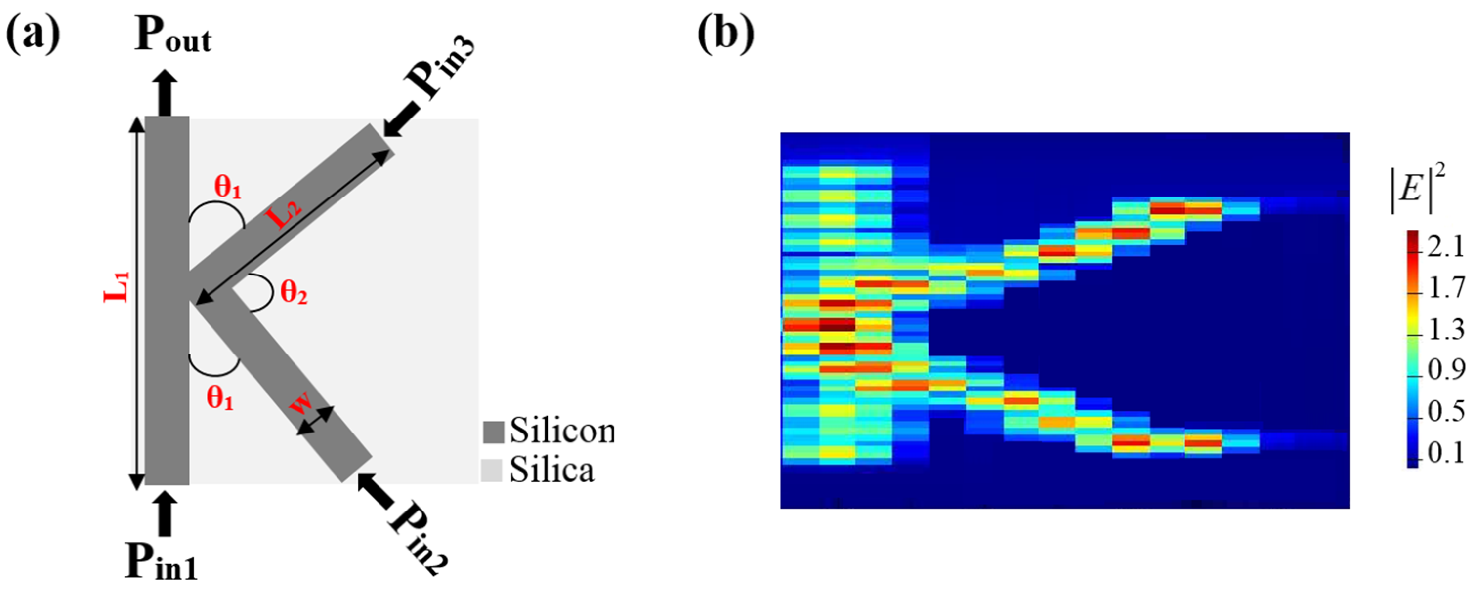
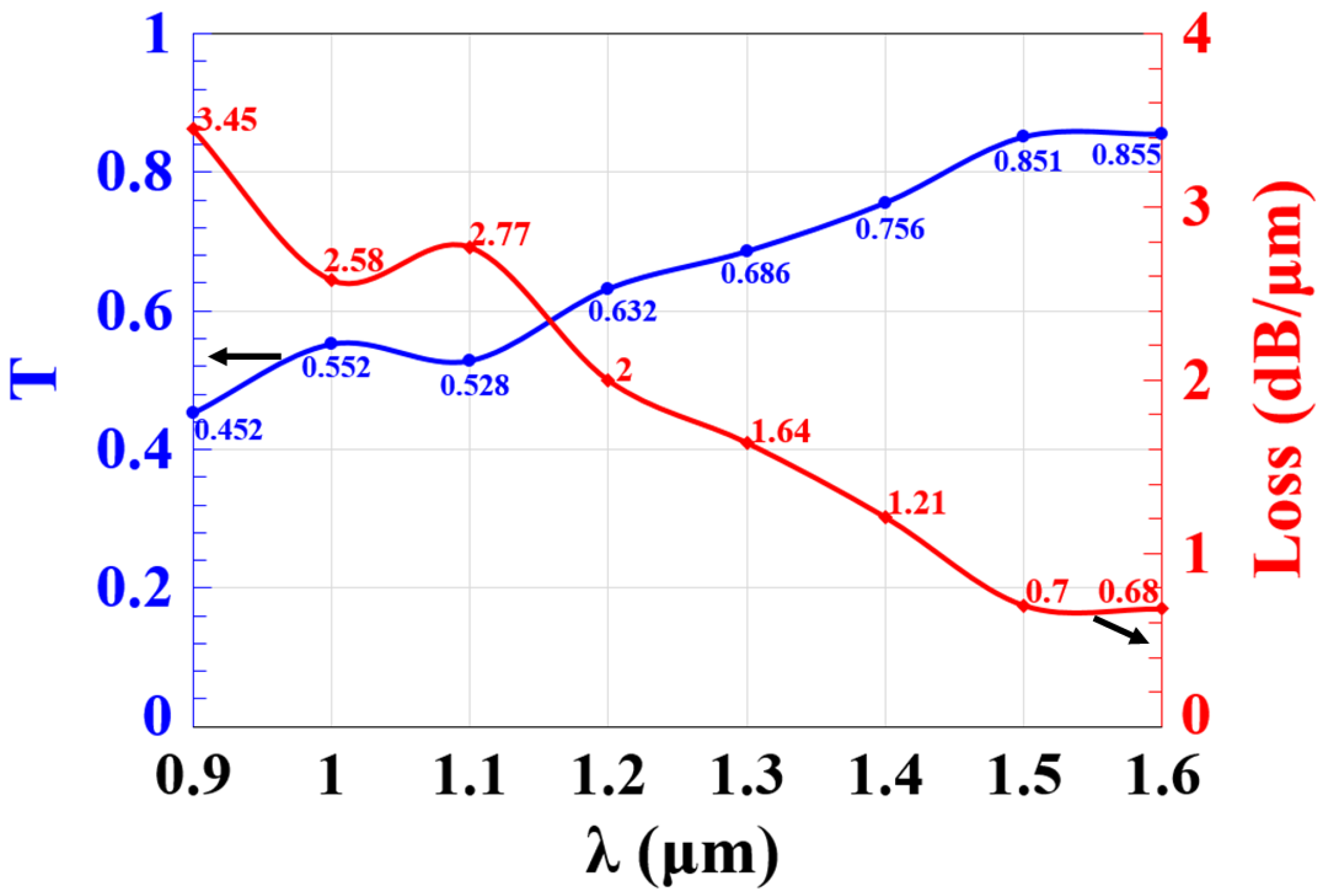
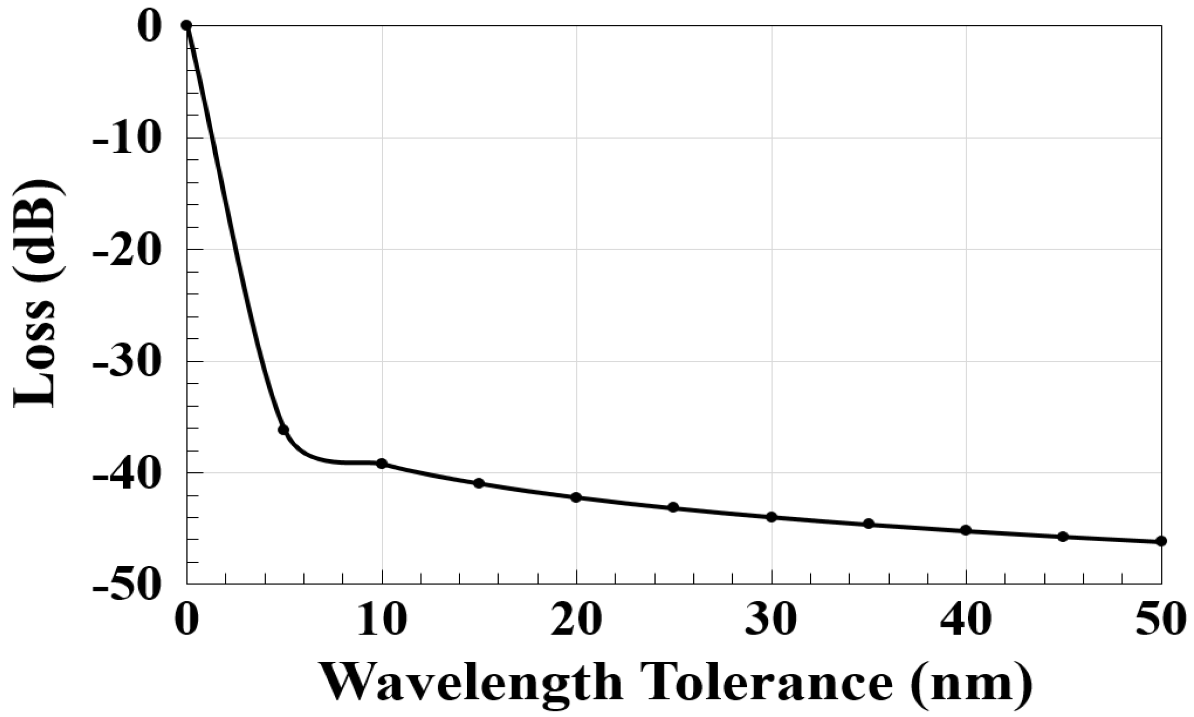
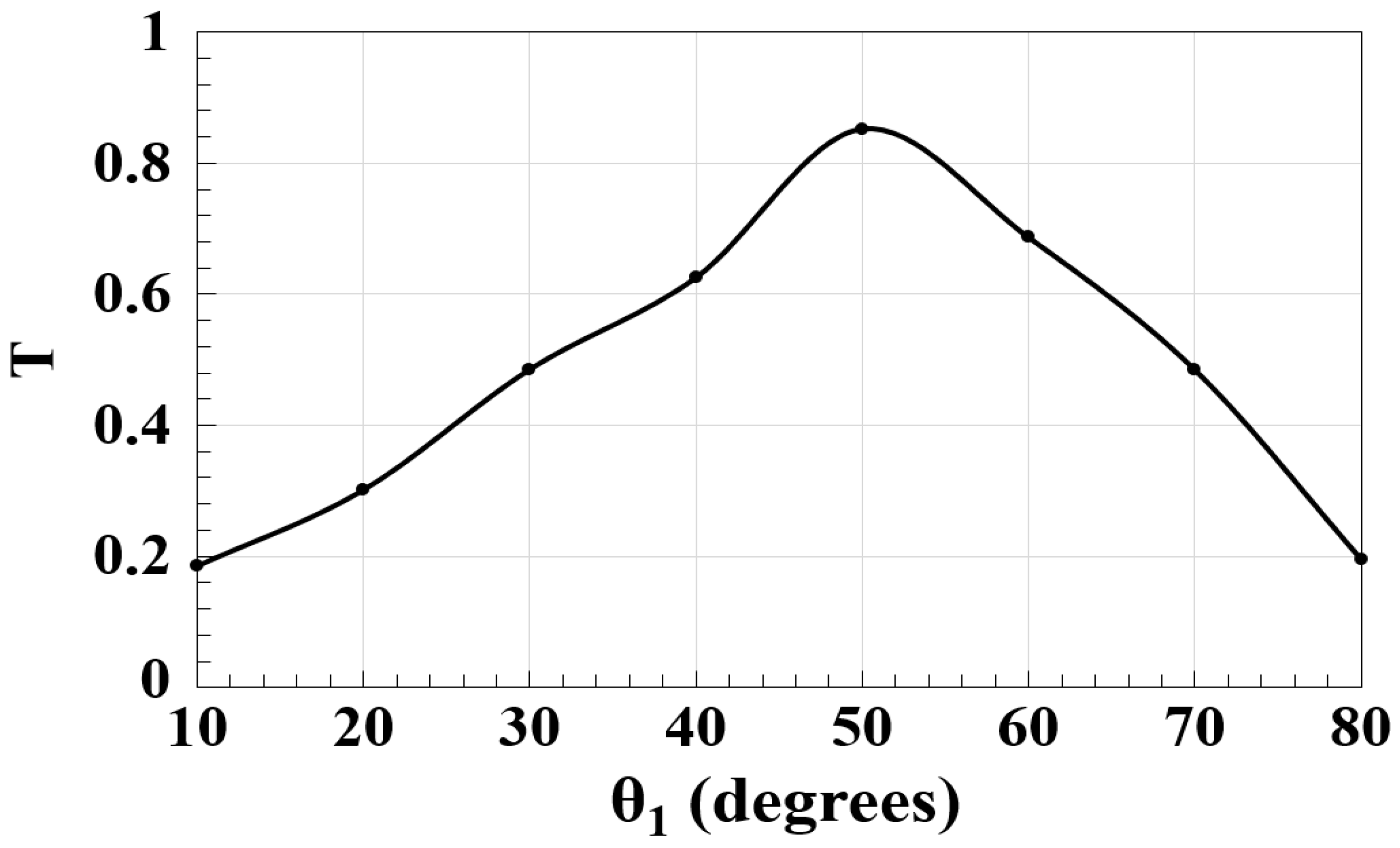
2. K-Shaped Waveguide
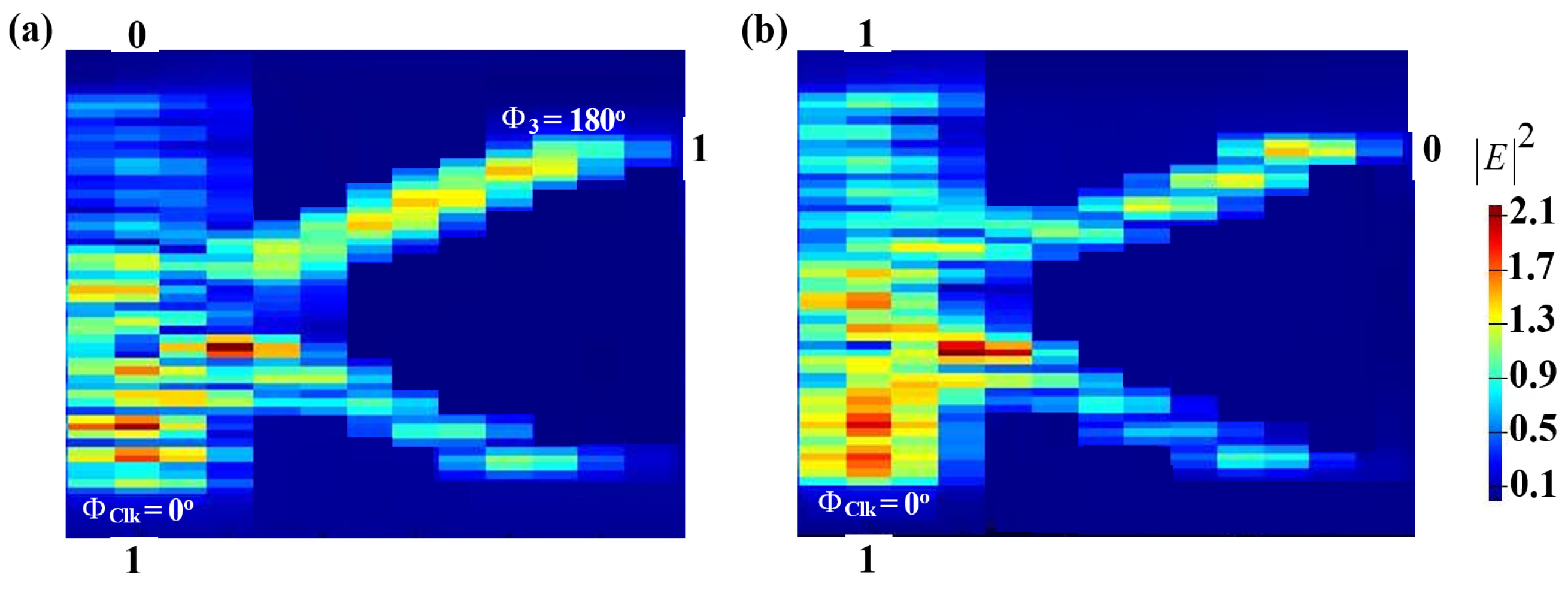
3. Logic Operations
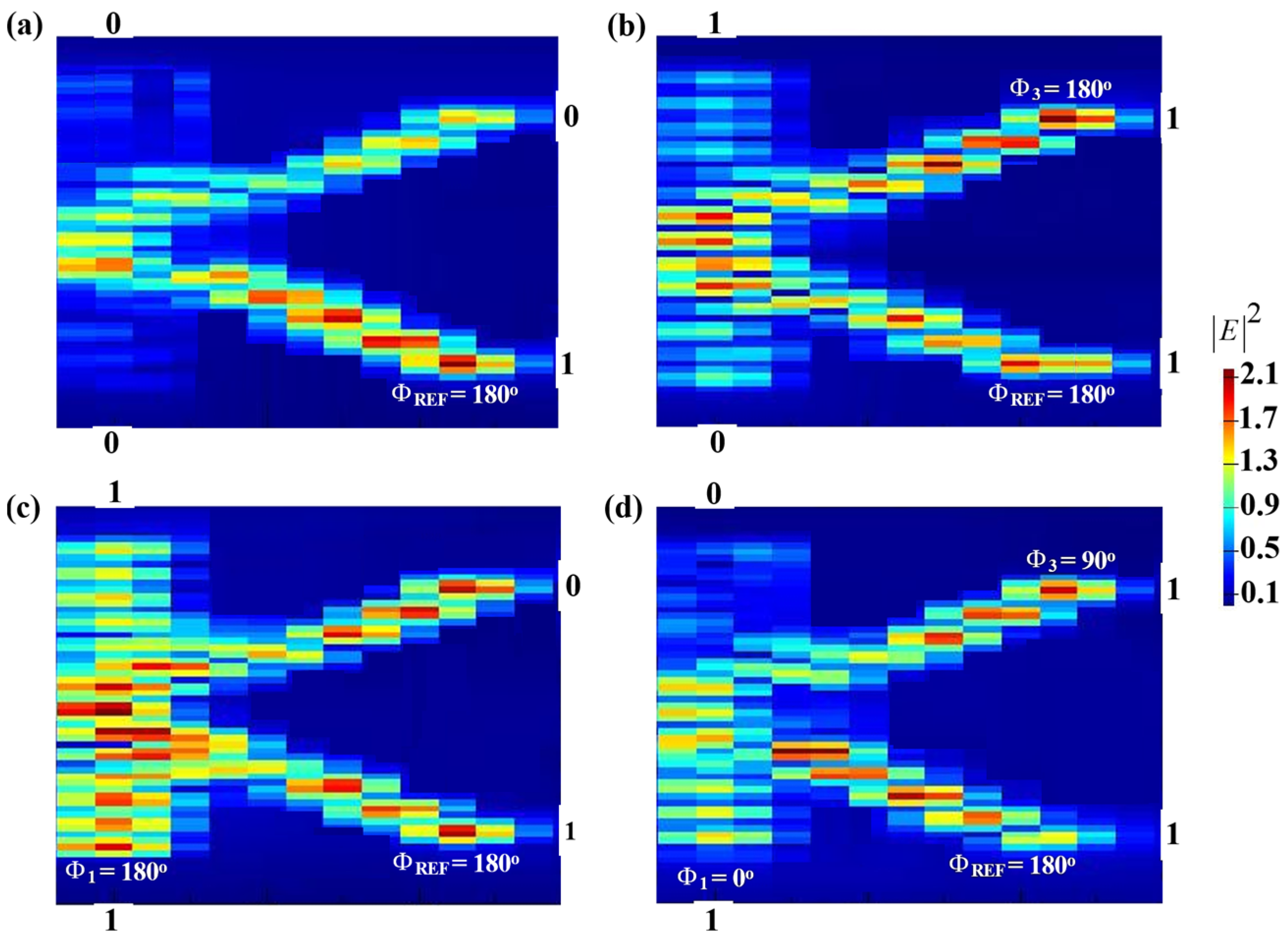
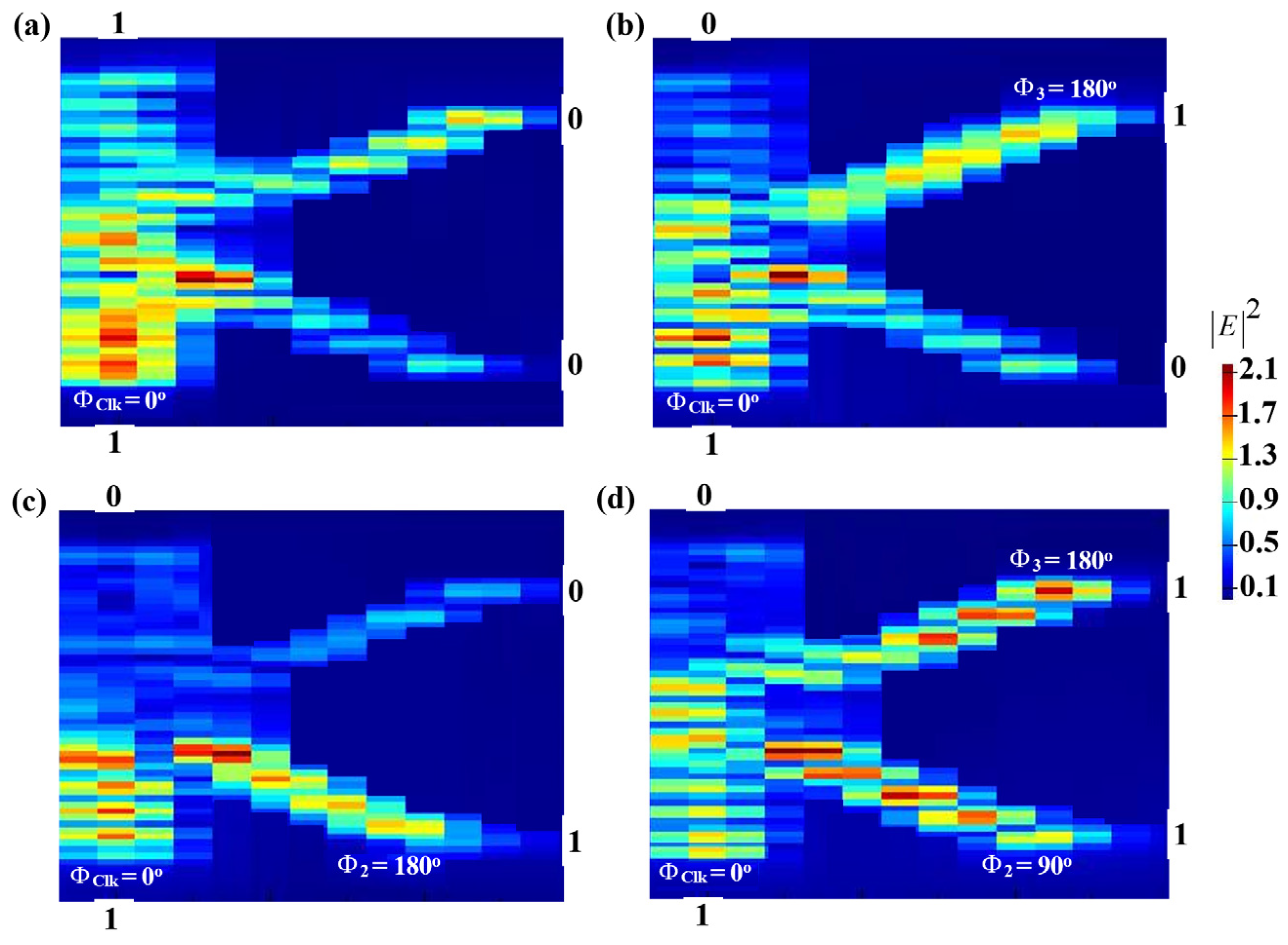
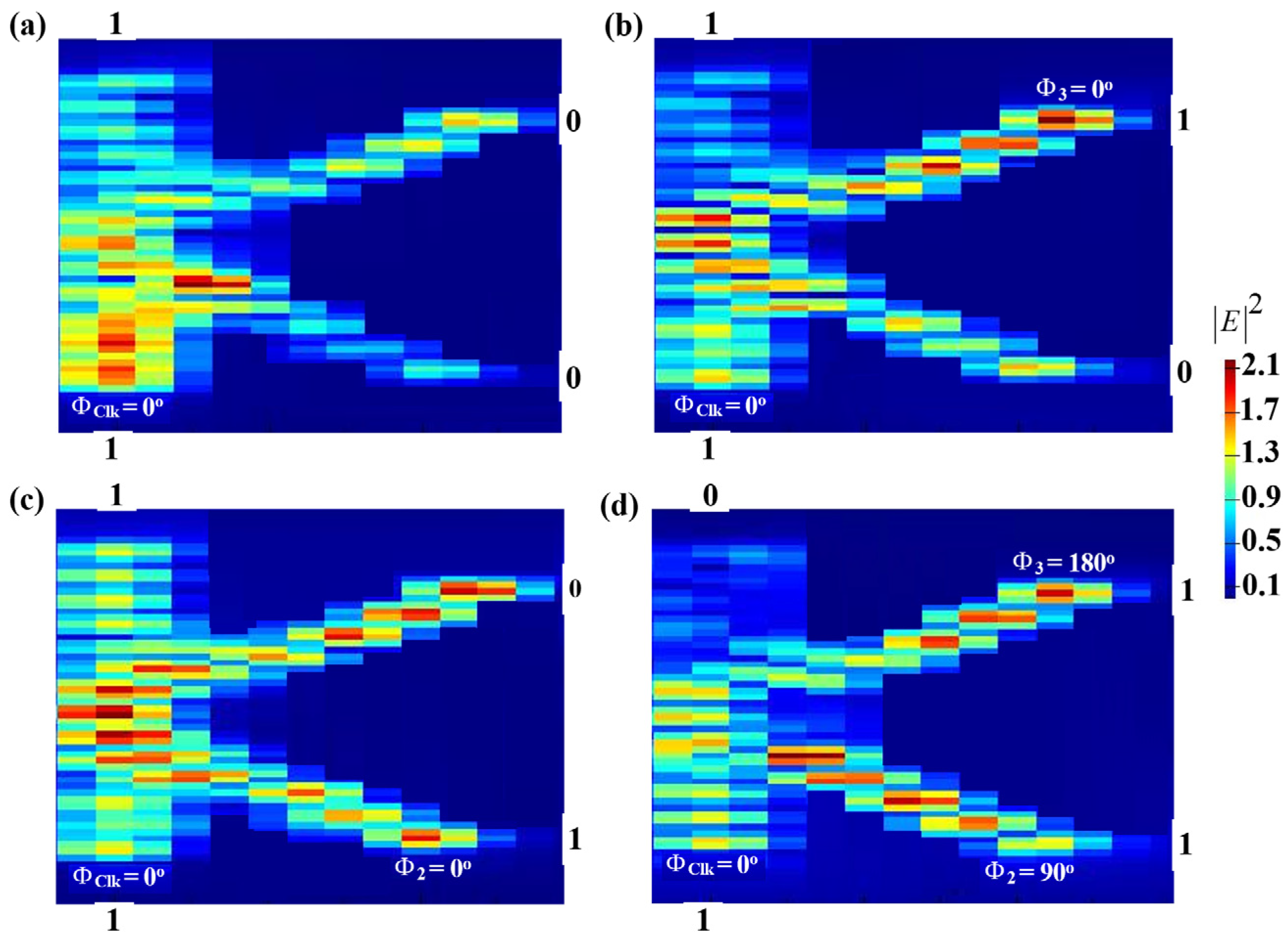
3.1. XOR
3.2. AND
3.3. OR
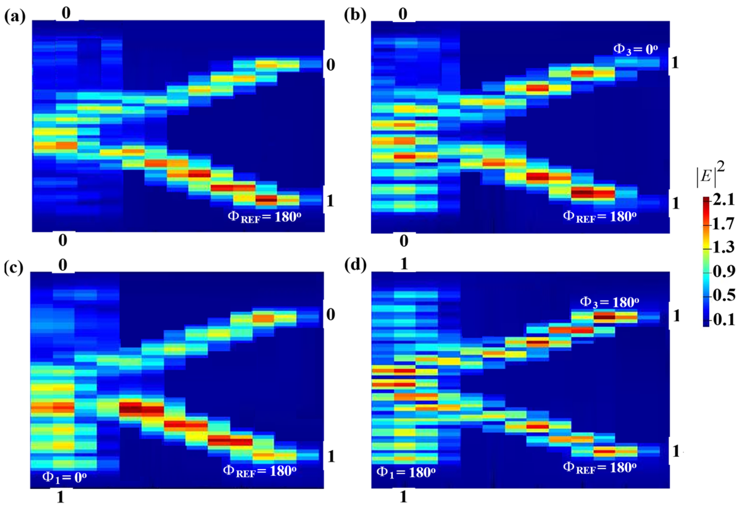
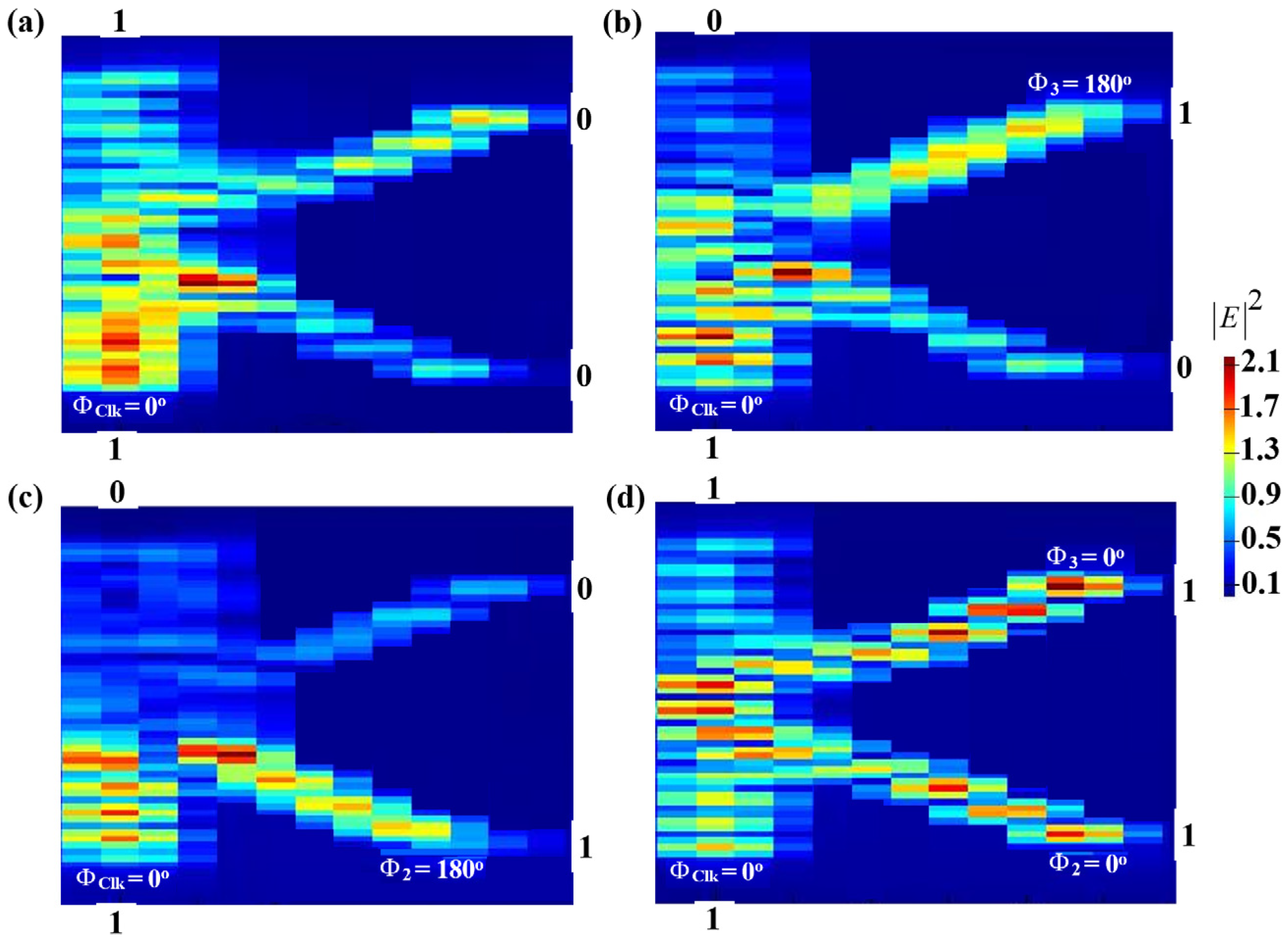
3.4. NOT
3.5. NOR
3.6. NAND
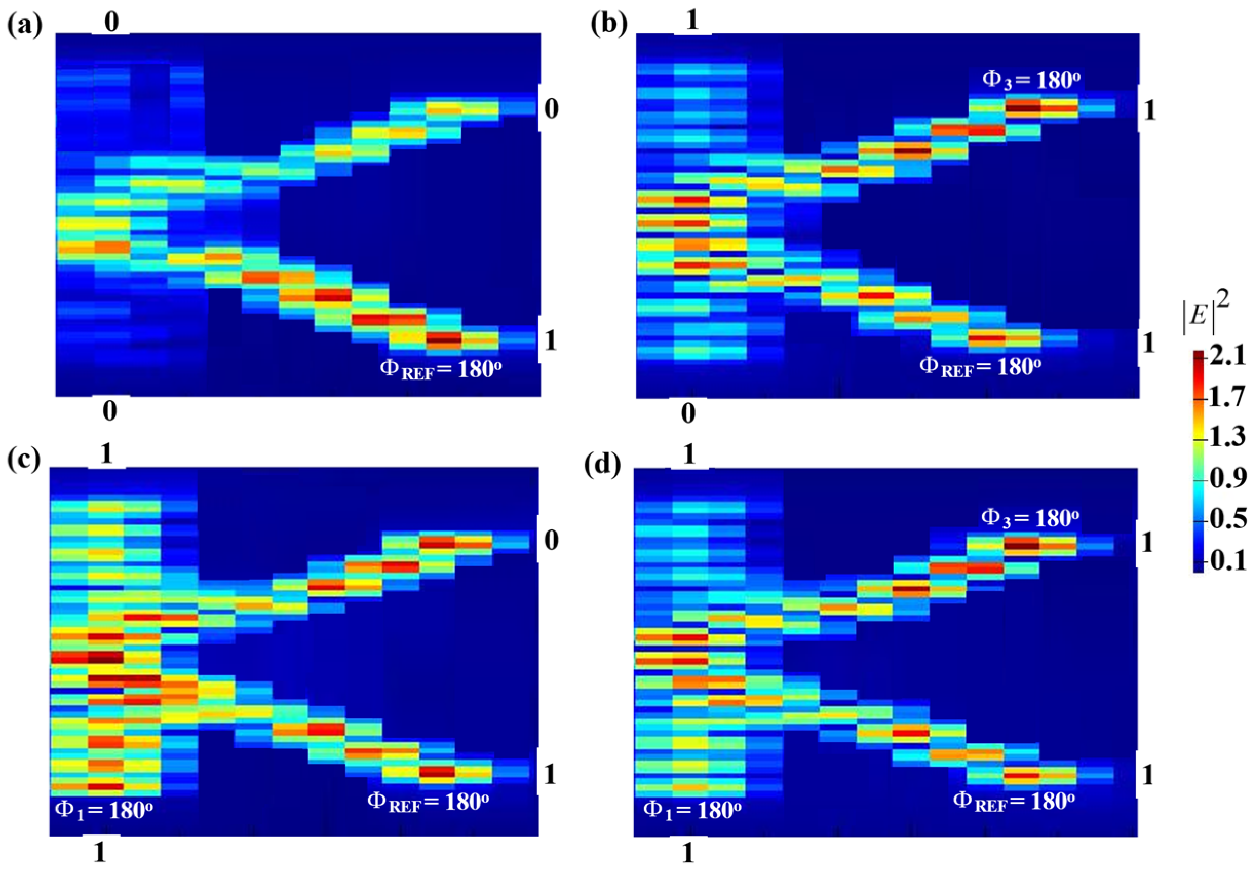
3.7. XNOR
4. Conclusions
Author Contributions
Funding
Data Availability Statement
Acknowledgments
Conflicts of Interest
References
- Houbavlis, C.; Zoiros, K.E.; Kalyvas, M.; Theophilopoulos, G.; Bintjas, C.; Yiannopoulos, K.; Pleros, N.; Vlachos, K.; Avramopoulos, H.; Schares, L.; et al. All-optical signal processing and applications within the Esprit project DO ALL. J. Lightwave Technol. 2005, 23, 781–801. [Google Scholar] [CrossRef]
- Clavero, R.; Mart´ınez, J.M.; Ramos, F.; Mart, J. All-optical packet routing scheme for optical label-swapping networks. Opt. Express 2004, 12, 4326–4332. [Google Scholar] [CrossRef] [PubMed]
- Ji, W.; Zhang, M.; Ye, P. All-optical-packet header and payload separation for unslotted optical-packet-switched networks. J. Lightwave Technol. 2007, 25, 703–709. [Google Scholar] [CrossRef]
- Ma, S.; Sun, H.; Chen, Z.; Dutta, N.K. High-speed all-optical PRBS generation based on quantum-dot semiconductor optical amplifiers. Opt. Express 2009, 17, 18469–18477. [Google Scholar] [CrossRef]
- Singh, S.; Lovkesh; Ye, X.; Kaler, R.S. Design of ultrafast encryption and decryption circuits for secured optical networks. IEEE J. Quantum Electron. 2012, 48, 1547–1553. [Google Scholar] [CrossRef]
- Aikawa, Y.; Shimizu, S.; Uenohara, H. Demonstration of all-optical divider circuit using SOA-MZI-type XOR gate and feedback loop for forward error detection. J. Lightwave Technol. 2011, 29, 2259–2266. [Google Scholar] [CrossRef]
- Kim, S.H.; Kim, J.H.; Choi, J.W.; Son, C.W.; Byun, Y.T.; Jhon, Y.M.; Lee, S.; Woo, D.H.; Kim, S.H. All-optical half adder using cross gain modulation in semiconductor optical amplifiers. Opt. Express 2006, 14, 10693–10698. [Google Scholar] [CrossRef]
- Gayen, D.K.; Bhattachryya, A.; Chattopadhyay, T.; Roy, J.N. Ultrafast all-optical half-adder using quantum-dot semiconductor optical amplifier-based Mach–Zehnder interferometer. J. Lightwave Technol. 2012, 30, 3387–3393. [Google Scholar] [CrossRef]
- Berrettini, G.; Nguyen, A.T.; Lazzeri, E.; Meloni, G.; Scaffardi, M.; Pot, L.; Bogoni, A. All-optical digital circuits exploiting SOA-based loop memories. IEEE J. Sel. Top. Quantum Electron. 2012, 18, 847–858. [Google Scholar] [CrossRef]
- Wang, Y.; Zhang, X.; Dong, J.; Huang, D. Simultaneous demonstration on all-optical digital encoder and comparator at 40 Gb/s with semiconductor optical amplifiers. Opt. Express 2007, 15, 15080–15085. [Google Scholar] [CrossRef]
- Scaffardi, M.; Ghelfi, P.; Lazzeri, E.; Pot, L.; Bogoni, A. Photonic processing for digital comparison and full addition based on semiconductor optical amplifiers. IEEE J. Sel. Top. Quantum Electron. 2008, 14, 826–833. [Google Scholar] [CrossRef]
- Zoiros, K.E.; Houbavlis, T.; Kalyvas, M. Ultra-high speed all-optical shift registers and their applications in OTDM networks. Opt. Quantum Electron. 2004, 36, 1005–1053. [Google Scholar] [CrossRef]
- Kumar, S.; Willner, A.E. Simultaneous four-wave mixing and cross-gain modulation for implementing an all-optical XNOR logic gate using a single SOA. Opt. Express 2006, 14, 5092–5097. [Google Scholar] [CrossRef] [PubMed]
- Jung, Y.J.; Son, C.W.; Jhon, Y.M.; Lee, S.; Park, N. One-level simplification method for all-optical combinational logic circuits. IEEE Photon. Technol. Lett. 2008, 20, 800–802. [Google Scholar] [CrossRef]
- Mashanovich, G.Z.; Milošević, M.M.; Nedeljkovic, M.; Owens, N.; Xiong, B.; Teo, E.J.; Hu, Y. Low loss silicon waveguides for the mid-infrared. Opt. Express 2011, 19, 7112–7119. [Google Scholar] [CrossRef] [Green Version]
- Yao, C.; Kotb, A.; Wang, B.; Singh, S.; Guo, C. All-optical logic gates using dielectric-loaded waveguides with quasi-rhombus metasurfaces. Opt. Lett. 2020, 45, 3769–3772. [Google Scholar] [CrossRef]
- Yanga, W.; Shi, X.; Xing, H.; Chen, X. All-optical logic gates based on metallic waveguide arrays. Res. Phys. 2018, 11, 837–841. [Google Scholar] [CrossRef]
- Abdulnabi, S.H.; Abbas, M.N. All-optical logic gates based on nanoring insulator–metal–insulator plasmonic waveguides at optical communications band. J. Nanophotonics 2019, 13, 016009. [Google Scholar] [CrossRef] [Green Version]
- Al-Musawi, H.K.; Al-Janabi, A.K.; Al-Abassi, S.A.W.; Abusiba, N.A.A.; Al-Fatlawi, N.A.Q. Plasmonic logic gates based on dielectric-metal-dielectric design with two optical communication bands. Optik 2020, 223, 165416. [Google Scholar] [CrossRef]
- Caballero, L.P.; Povinelli, M.L.; Ramirez, J.C.; Guimarães, P.S.S.; Neto, O.P.V. Photonic crystal integrated logic gates and circuits. Opt. Express 2022, 30, 1976. [Google Scholar] [CrossRef]
- Asakawa, K.; Sugimoto, Y.; Nakamura, S. Silicon photonics for telecom and data-com applications. Opto-Electron. Adv. 2020, 3, 200011. [Google Scholar] [CrossRef]
- Sun, C.; Yu, Y.; Zhang, X. Ultra-compact waveguide crossing for a mode-division multiplexing optical network. Opt. Lett. 2017, 42, 4913–4916. [Google Scholar] [CrossRef] [PubMed]
- Green, W.M.J.; Rooks, M.J.; Sekaric, L.; Vlasov, Y.A. Ultra-compact, low RF power, 10 Gb/s silicon Mach-Zehnder modulator. Opt. Express 2007, 15, 17106–17113. [Google Scholar] [CrossRef] [PubMed]
- Dimitropoulos, D.; Raghunathan, V.; Claps, R.; Jalali, B. Phase-matching and nonlinear optical processes in silicon waveguides. Opt. Express 2004, 12, 149–160. [Google Scholar] [CrossRef] [Green Version]
- Kotb, A.; Guo, C. 100 Gb/s all-optical multifunctional AND, XOR, NOR, OR, XNOR, and NAND logic gates in a single compact scheme based on semiconductor optical amplifiers. Opt. Laser Technol. 2021, 137, 106828. [Google Scholar] [CrossRef]
- Zoiros, K.E.; Papadopoulos; Houbavlis, T.; Kanellos, G.T. Theoretical analysis and performance investigation of ultrafast all-optical Boolean XOR gate with semiconductor optical amplifier-assisted Sagnac interferometer. Opt. Commun. 2006, 258, 114–134. [Google Scholar] [CrossRef]
- Passaro, V.M.N.; Notte, M.L. Optimizing SOI slot waveguide fabrication tolerances and strip-slot coupling for very efficient optical sensing. Sensors 2012, 12, 2436–2455. [Google Scholar] [CrossRef] [Green Version]
- Prinzen, A.; Waldow, M.; Kurz, H. Fabrication tolerances of SOI based directional couplers and ring resonators. Opt. Express 2013, 21, 17212–17220. [Google Scholar] [CrossRef]
- Available online: https://www.edmundoptics.com/p/1550nm-0-250mw-fiber-coupled-laser/12219/ (accessed on 13 November 2022).
- Al-Hetara, A.M.; Shamsan, Z.A. Optical wavelength and dimensions tolerance criterion for multimode interference couplers. WSEAS Trans. Commun. 2014, 13, 567–571. [Google Scholar]
- Kita, S.; Nozaki, K.; Takata, K.; Shinya, A.; Notomi, M. Ultrashort low-loss Ψ gates for linear optical logic on Si photonics platform. Commun. Phys. 2020, 3, 33. [Google Scholar] [CrossRef] [Green Version]
- Donzella, V.; Sherwali, A.; Flueckiger, J.; Grist, S.M.; Fard, S.T.; Chrostowski, L. Design and fabrication of SOI micro-ring resonators based on sub-wavelength grating waveguides. Opt. Express 2015, 23, 4791–4803. [Google Scholar] [CrossRef] [PubMed]
- Pan, D.; Wei, H.; Xu, H. Optical interferometric logic gates based on metal slot waveguide network realizing whole fundamental logic operations. Opt. Express 2013, 21, 9556. [Google Scholar] [CrossRef] [PubMed] [Green Version]
- Gao, L.; Chen, L.; Wei, H.; Xu, H. Lithographically fabricated gold nanowire waveguides for plasmonic routers and logic gates. Nanoscale 2018, 10, 14771. [Google Scholar] [CrossRef] [PubMed] [Green Version]
- Fu, Y.; Hu, X.; Lu, C.; Yue, S.; Yang, H.; Gong, Q. All-optical logic gates based on nanoscale plasmonic slot waveguides. Nano Lett. 2012, 12, 5784–5790. [Google Scholar] [CrossRef] [PubMed]
- Hou, Z.; Sun, Y.; Li, Q.; Xudong, F.; Cheng, R. Smart bio-gel optofluidic Mach–Zehnder interferometers multiphoton-lithographically customized with chemo-mechanical-opto transduction and bio-triggered degradation. Lab Chip 2020, 20, 3815–3823. [Google Scholar] [CrossRef]
- Liang, D.; Zhang, X.; Li, M.; Lin, Z.; Dai, H.; Wu, Z.; Pu, J. Visually Adjusting Coupling Conditions in Light-Emitting Micro-Components. IEEE Photon. Technol. Lett. 2019, 31, 1425–1428. [Google Scholar] [CrossRef]
- Kowsari, A.; Saghaei, H. Resonantly enhanced all-optical switching in microfibre Mach–Zehnder interferometers. Electron. Lett. 2018, 54, 229–231. [Google Scholar] [CrossRef]


| Symbol | Definition | Value | Unit |
|---|---|---|---|
| L1 | Length of long slot | 2.5 | μm |
| L2 | Length of short slot | 1.0 | μm |
| W | Width of slot | 0.22 | μm |
| D | Thickness of slot | 0.3 | μm |
| θ1 | Angle between long and short slots | 50 | degree |
| θ2 | Angle between short slots | 80 | degree |
| nsilicon | Silicon refractive index at 1.55 μm | 3.48 | - |
| nsilica | Silica refractive index at 1.55 μm | 1.444 | - |
| λ | Operating wavelength | 1.55 | μm |
| Tth | Threshold transmission | 0.12 | - |
| Pin1 | Pin3 | Pin2 (REF) | T | Pout | CR (dB) |
|---|---|---|---|---|---|
| 0 | 0 | 1 | 0.021 | 0 | 34 |
| 0 | 1 | 1 | 0.464 | 1 | |
| 1 | 0 | 1 | 0.852 | 1 | |
| 1 | 1 | 1 | 0.023 | 0 |
| Pin1 | Pin3 | Pin2 (REF) | T | Pout | CR (dB) |
|---|---|---|---|---|---|
| 0 | 0 | 1 | 0.021 | 0 | 31 |
| 0 | 1 | 1 | 0.022 | 0 | |
| 1 | 0 | 1 | 0.023 | 0 | |
| 1 | 1 | 1 | 0.521 | 1 |
| Pin1 | Pin3 | Pin2 (REF) | T | Pout | CR (dB) |
|---|---|---|---|---|---|
| 0 | 0 | 1 | 0.021 | 0 | 33.73 |
| 0 | 1 | 1 | 0.464 | 1 | |
| 1 | 0 | 1 | 0.852 | 1 | |
| 1 | 1 | 1 | 0.521 | 1 |
| Operation | CR (dB) with REF | CR (dB) without REF |
|---|---|---|
| XOR | 34 | 7.1 |
| AND | 31 | 6.4 |
| OR | 33.73 | 7 |
| Pin1 (Clk) | Pin3 | T | Pout | CR (dB) |
|---|---|---|---|---|
| 1 | 1 | 0.032 | 0 | 30.5 |
| 1 | 0 | 0.675 | 1 |
| Pin1 (Clk) | Pin2 | Pin3 | T | Pout | CR (dB) |
|---|---|---|---|---|---|
| 1 | 0 | 0 | 0.675 | 1 | 33 |
| 1 | 0 | 1 | 0.032 | 0 | |
| 1 | 1 | 0 | 0.022 | 0 | |
| 1 | 1 | 1 | 0.022 | 0 |
| Pin1 (Clk) | Pin2 | Pin3 | T | Pout | CR (dB) |
|---|---|---|---|---|---|
| 1 | 0 | 0 | 0.675 | 1 | 34 |
| 1 | 0 | 1 | 0.464 | 1 | |
| 1 | 1 | 0 | 0.852 | 1 | |
| 1 | 1 | 1 | 0.022 | 0 |
| Pin1 (Clk) | Pin2 | Pin3 | T | Pout | CR (dB) |
|---|---|---|---|---|---|
| 1 | 0 | 0 | 0.675 | 1 | 31 |
| 1 | 0 | 1 | 0.032 | 0 | |
| 1 | 1 | 0 | 0.022 | 0 | |
| 1 | 1 | 1 | 0.521 | 1 |
| Operations | Design | Wavelength (nm) | CR (dB) | Ref. |
|---|---|---|---|---|
| XOR, AND, OR, NOR, NAND, XNOR | Dielectric-loaded waveguides | 471 | 24.41–33.39 | [16] |
| OR, NOT, AND, XOR | Metallic waveguide arrays | 632.8 | 9.3–20 | [17] |
| NOT, XOR, AND, OR, NOR, NAND, XNOR | Nanoring insulator–metal–insulator waveguides | 1550 | −1.1–18.75 | [18] |
| NOT, XOR, AND, OR, NOR, NAND, XNOR | Dielectric–metal–dielectric design | 900 and 1330 | 5.37–22 | [19] |
| AND, OR, NAND, NOR, XOR, Fan-Out, Half adder, Full adder | Photonic crystal circiuts | 1550 | 5.54–11.56 | [20] |
| XOR, AND, OR, NOT, NOR, XNOR, NAND | K-shaped silicon waveguides | 1550 | 30.5–34 | This work |
Publisher’s Note: MDPI stays neutral with regard to jurisdictional claims in published maps and institutional affiliations. |
© 2022 by the authors. Licensee MDPI, Basel, Switzerland. This article is an open access article distributed under the terms and conditions of the Creative Commons Attribution (CC BY) license (https://creativecommons.org/licenses/by/4.0/).
Share and Cite
Kotb, A.; Zoiros, K.E. K-Shaped Silicon Waveguides for Logic Operations at 1.55 μm. Electronics 2022, 11, 3748. https://doi.org/10.3390/electronics11223748
Kotb A, Zoiros KE. K-Shaped Silicon Waveguides for Logic Operations at 1.55 μm. Electronics. 2022; 11(22):3748. https://doi.org/10.3390/electronics11223748
Chicago/Turabian StyleKotb, Amer, and Kyriakos E. Zoiros. 2022. "K-Shaped Silicon Waveguides for Logic Operations at 1.55 μm" Electronics 11, no. 22: 3748. https://doi.org/10.3390/electronics11223748