Article

A 60GS/s Two-Stage Sampler with a Linearity Calibration Loop for PAM-8 Receivers

1
Department of Information Engineering, University of Pisa, 56122 Pisa, Italy
2
Marvell Semiconductor, 27100 Pavia, Italy
*
Author to whom correspondence should be addressed.
Electronics 2022, 11(21), 3484; https://doi.org/10.3390/electronics11213484
Submission received: 6 October 2022 / Revised: 21 October 2022 / Accepted: 24 October 2022 / Published: 27 October 2022
(This article belongs to the Special Issue Design and Applications of Nonlinear Circuits and Systems)

Abstract

:
In this article, we show a 60 GS/s two-stage 8 × 8 time-interleaved sampling circuit, where the second-stage nonlinearity can be controlled by using the voltage that optimizes the static distortions of the sampler. A calibration algorithm can extract the nonlinear contributions of the stages and compensate for them by setting the optimal bias voltage. This can also be used to cancel the front-end nonlinear effects. The sampler was verified by implementing it in TSMC 5 nm FinFET, and a calibration system in a Pulse Amplitude Modulation transceiver, detecting and minimizing the nonlinearities, is presented. The optimum voltage biasing of the sampler was obtained by co-simulating the circuit with the linearity calibration loop implemented in Verilog-A. The histogram of the sampled signal at the slicer input is shown before and after the calibration to show the improvement in the sampled eye opening. Moreover, the resulting bias is equal to the one that maximizes the total harmonic distortion in transient simulations with a 1 GHz input signal, obtaining a minimum of 48.5 dB of total harmonic distortion across different PVT conditions.

1. Introduction

Over the last decade, data traffic has increased due to the increasing demand for streaming services, video calling, etc., implying the necessity for high-speed transceivers for either backplane or optic fiber communications in data centers. Pulse Amplitude Modulation with four levels (PAM-4) [1,2,3] is the main modulation used in wire-line transceivers, in which there are four symbols, each one representing two bits. To further improve the data rate, we can either boost the symbol rate, with the heavy constraint imposed by the channel bandwidth, or increase the order of the modulation. Some solutions can be the PAM-8 [4,5,6] or another modulation using more than four symbols [7]. In particular, while sending the same number of symbols per second, the PAM-8 improves the bit rate of the receiver by 1.5 times. However, the smaller eye aperture of PAM-8 compared to PAM-4 or Non-Return-to-Zero (NRZ) makes this modulation format very sensitive to noise, distortions, and residual inter-symbol interference (ISI). These effects increase the bit error rate of the system. The ISI and the noise can be reduced with higher current consumption (less noisy analog components and a feed forward equalizer with a higher number of taps). On the other hand, the distortions are not easy to minimize. With the reduction in the supply voltage in advanced technology nodes, the circuits increment their compressing behavior on the signal (lower total harmonic distortion (THD)) for the same dynamic range, needed to maintain a valid signal-to-noise Ratio (SNR). In 
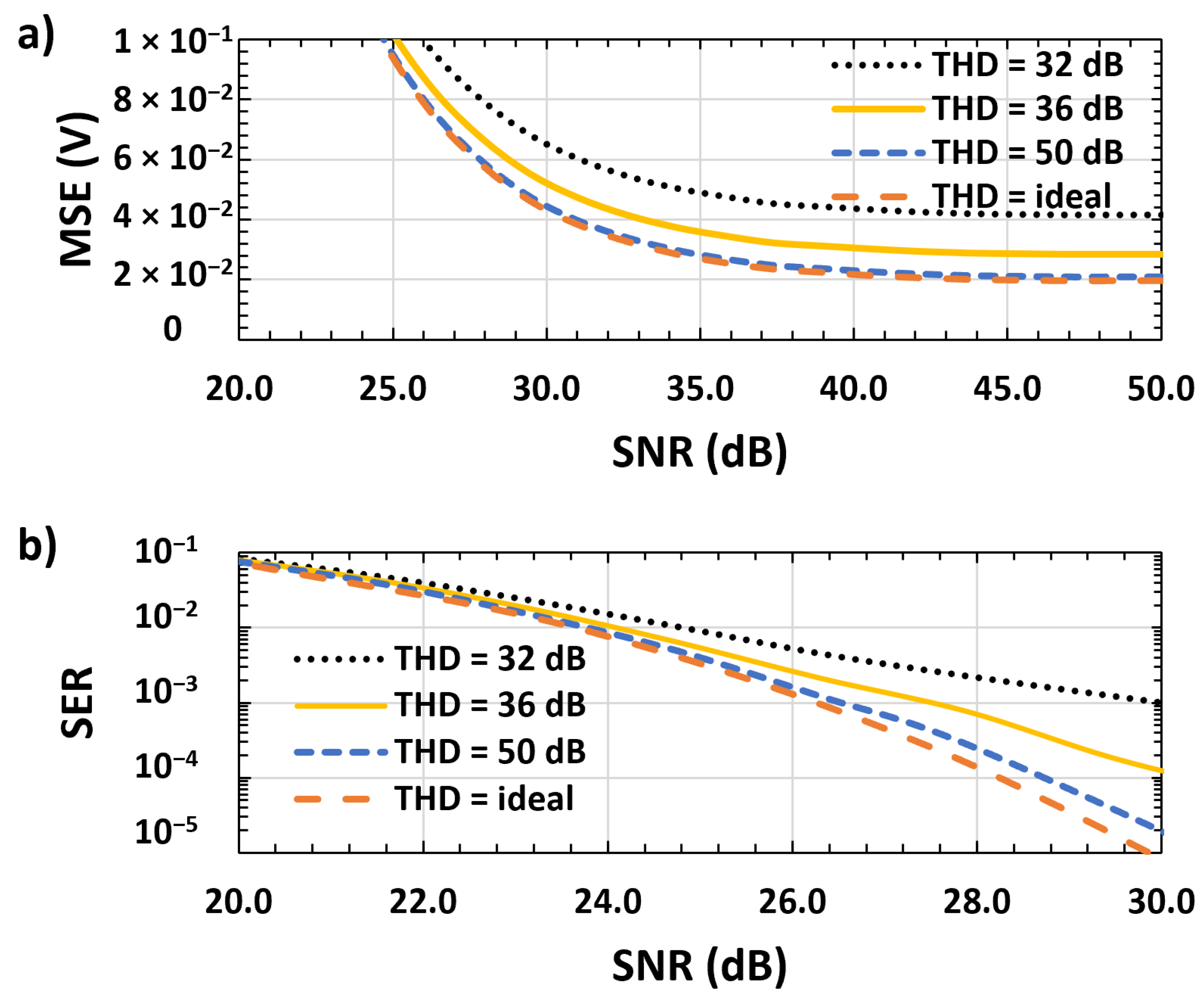
Figure 1, (a) the symbol error rate (SER) and (b) the mean square error (MSE) are plotted to the varying SNR for various analog front-end (AFE) THD obtained through a MATLAB model of a PAM-8 receiver, as in [8]. The THD represents the static nonlinearities modeled with a Taylor approximation of the components’ input–output characteristics. While this model has some limitations, it shows how linearity affects the system performance in some scenarios. The plots show an improvement in the MSE and SER for higher THD values and performance approaching the ideal case for 50 dB, meaning this value should be a target for the analog circuit design.
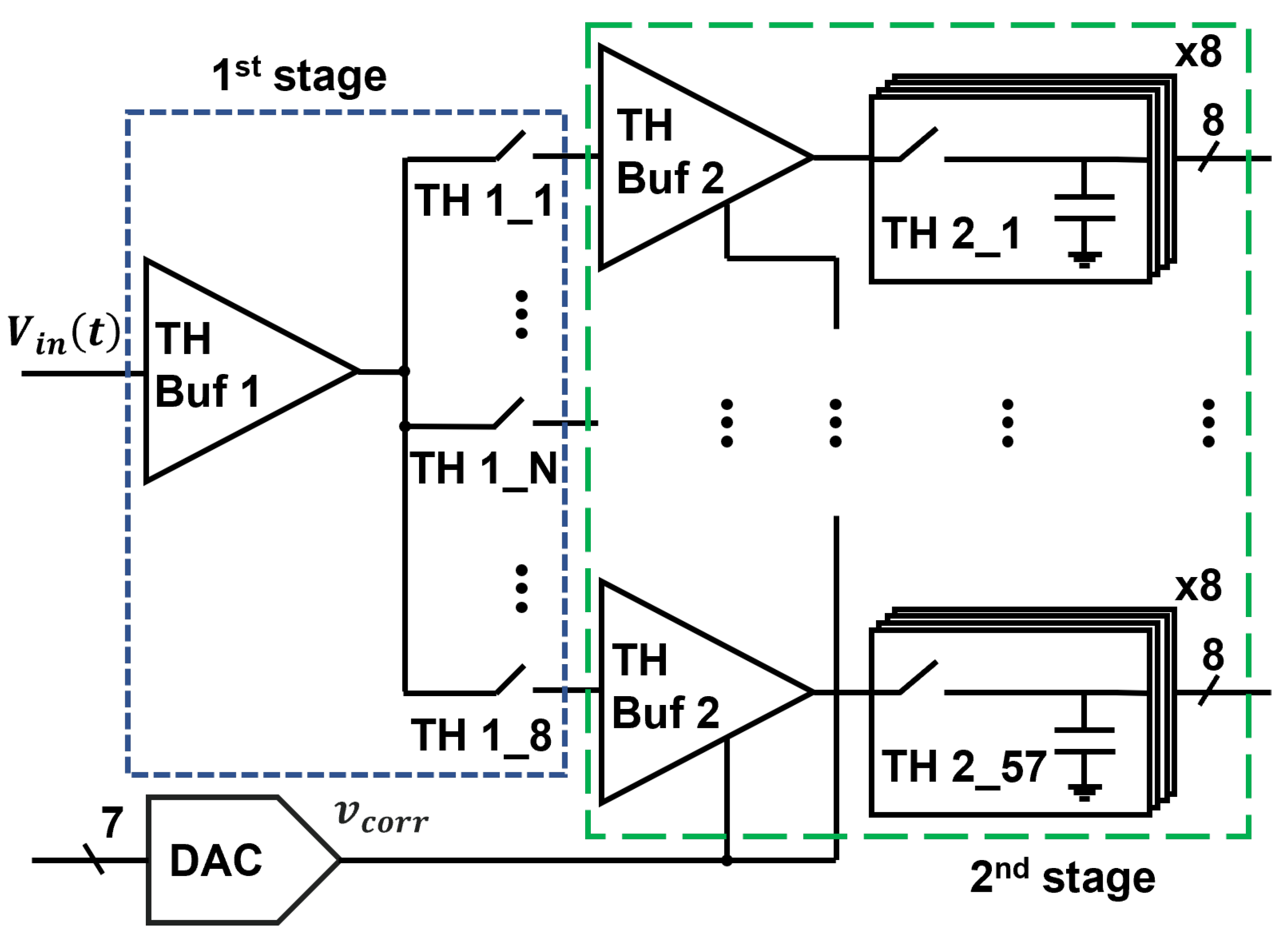
To maximize the system performance, the THD, especially of critical blocks such as the track and hold (TH) of time-interleaved (TI) receivers, needs to be optimized through calibration as a consequence of the low circuit linearity across PVT in scaled technology nodes. This solution is normally adopted in the reduction in distortions derived from the interleaved channels mismatches [9,10]. In the literature, the calibration of static distortion is rare [11,12], and no co-simulation nor indepth modeling of AFE components is introduced in the system simulation. The scope of this paper is to find a TI-TH circuit capable of achieving through calibration a receiver THD of the order of 50 dB across different PVT conditions to maximize the performance of a PAM-8 receiver (RX). Here, we show the TI sampler presented in [8] using an improved and simpler calibration loop compared to the cited one, where the complexity scales with the number of nonnegligible residual ISI pre- and post-cursors, and a gain error can introduce a component that does not let the system set to the desired value. The proposed loop uses an algorithm that eliminates the errors given by the gain and residual ISI while having a fixed complexity. Furthermore, this improved calibration was implemented in cadence virtuoso with a Verilog-A model, and its performance was verified via co-simulation with the analog circuit, while in [8] MATLAB, modeling of the analog was used.
This work is divided into three major sections. First, in Section 2, the implemented track-and-hold circuit is described, and its linear behavior with the control voltage is shown. Then, the calibration feedback loop is proposed and its analytical functioning is described in Section 3. Lastly, Virtuoso co-simulation of the transistor-level TH circuit and Verilog-A receiver model were performed, and the simulation results are presented in Section 4.

2. Track-And-Hold Circuit

The diagram in Figure 2 depicts the architecture used for implementing the 64 TI sampler, sampling at 60 GS/s. The interleaving factor was obtained by using a cascade of two TI stages ( 8 × 8 ) working at 7.5 GS/s and 937.5 MS/s, respectively.

2.1. Circuit Implementation

The circuit described in [13], which implements the first sampling stage (TH buf1), samples the signal on one of eight capacitances at a time. One input signal sample is taken every 16.7 ps. A buffer (TH buf2) is then connected to each sampling capacitance. To implement the second stage interleaving operation, eight parallel switches are connected to the output of the second buffer. The switches are operated to sample the signal on one of the eight sampling capacitances at a time. The buffers composing the second stage sampler can be implemented with the circuits in [14,15], composed of an inverter followed by another one closed in a diode configuration. These circuits show good linearity because while the inverter decompresses the signal, the second one has an opposite behavior, compensating for each other’s distortions. This approach has some limitations across process corners and temperatures stemming from the different variations of the linearity of the two blocks. To deal with this problem, we use the buffer topology depicted in Figure 3. The simple gm–gm topology is improved by varying the diode nonlinearity through the voltage v c o r r , as in [8]. An optimal value of the gate voltage can be chosen to minimize the distortions of the front end.

2.2. Buffer Distortion Control

An easy way to understand how the distortion of the buffer varies for various values of v c o r r is to plot, as shown in Figure 4, the relative error ( ϵ r ) between the small signal gain for high-DC differential input V S and the one for zero-DC differential input in different bias conditions:
ε r = V o u t d ( V S ) G A C V i n d ( V S = 0 ) G A C V i n d ( V S = 0 )
with G A C being the small-signal DC gain, V o u t d the differential small signal output, and V i n d the input one. By tuning v c o r r , the input–output characteristic of the buffer can compensate not just for the buffer distortion but also for the static nonlinearities of the previous stages and AFE as well. This is represented in Figure 3, where the input–output characteristic of the AFE plus the first-stage sampler is schematized with the typical compressing behavior, and where the second-stage buffer with behavior that compensates for this compression is introduced. Unfortunately, the optimal v c o r r for different PVT conditions may have considerable variations, thus a calibration that tracks the nonlinearities of the circuit becomes mandatory.
A further benefit of the calibration approach is that it may be able to identify the distortions of all the AFE and TH and maximize the THD performance of the system.

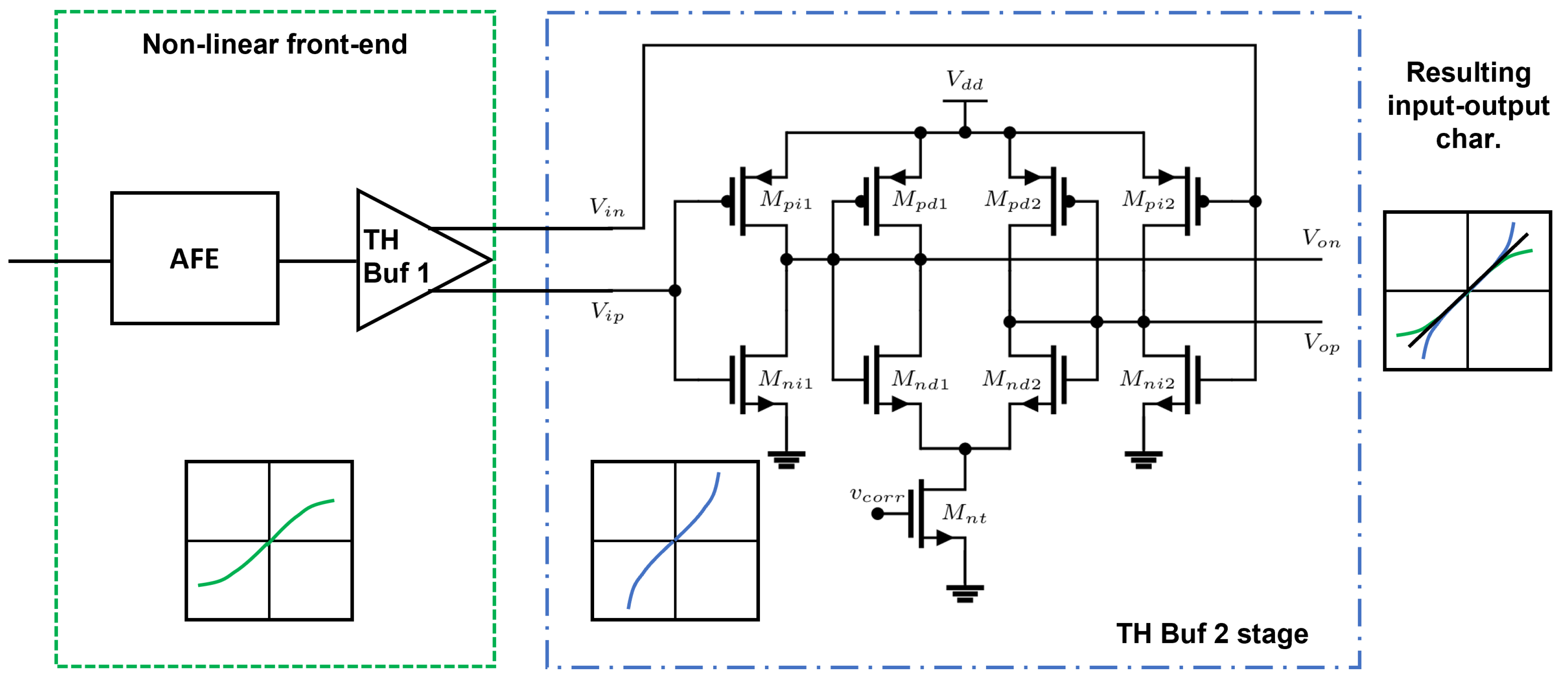
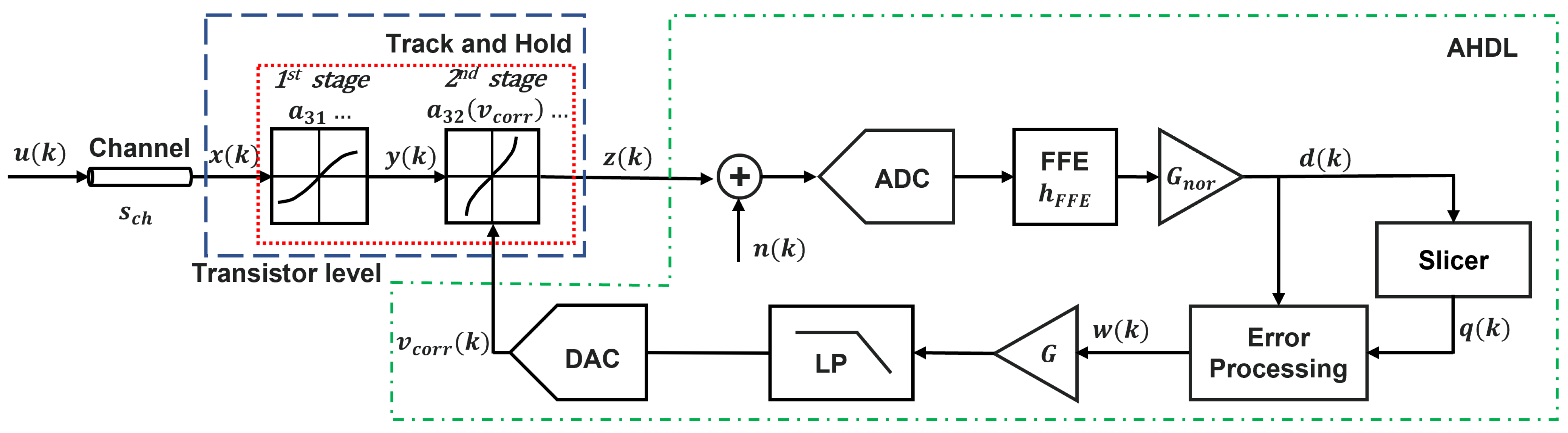
3. Linearity Calibration Feedback Loop

In this section, we present a calibration loop that is suitable for a PAM-8 receiver. The PAM-8 receiver model used is represented in Figure 5. The transmitter, the channel (IEEE ‘802.3ck Ch2M - lim_3ck_01_ 0319_c2m_Channel6’ with 30 dB loss at 30 GHz), and the AFE transfer functions were modeled with the channel symbol. Their combined s parameters matrix ( s c h ) filters the transmitted symbols and then feeds them to the two stages TH. In the analytical discussion of the model, the input–output characteristics that reflect the buffers’ static distortions were modeled using a Taylor polynomial [8,11,12], which depended on v c o r r in the second stage. For validation, the actual circuit was used.
Before the signal was sampled by the ADC, the thermal noise was inserted. Then, the ISI introduced by the channel was reduced using a Feed-Forward Equalizer (FFE). The slicer converted soft decisions into hard decisions, and by proper digital processing of this information, the optimum value of v c o r r was obtained. We used an ideal model to implement the DAC and ADC. The typical analog-to-digital converter can have a spurious free dynamic range (SFDR) of the order of 56 dB [16], which is negligible compared to the THD of the TI-TH circuit. The digital-to-analog converter only requires a monotone input–output characteristic due to the loop’s high gain capable of absorbing the small error derived from its nonlinearities. To better explain the mathematical operations, we take for granted that the circuit samples the signal on the optimum phase; hence, we assume the system works in a discrete time domain, and the channel was modeled with its impulsive response.
The signal sent by the transmitter u ( k ) was convoluted with the channel impulse response obtaining x ( k ) = G c h u ( k ) h c h ( k ) , where h c h is the equivalent impulse response of s c h , and G c h is the equivalent channel gain. After the distortion introduced by the TH circuit, we have:
z ( k ) = x ( k ) + a 3 x 3 ( k ) + a 5 x 5 ( k ) + a 7 x 7 ( k )
with a i being the Taylor coefficients of the overall analog front end, assuming the nonlinearities can be described with a Taylor expansion of the input–output characteristics. If we assume the FFE is optimal and we neglect the residual ISI, d ( k ) can be written as:
d ( k ) = u ( k ) + G n o r [ a 3 x 3 ( k ) + a 5 x 5 ( k ) + a 7 x 7 ( k ) + n ( k ) ] h F F E ( k )
with n ( k ) being the equivalent analog circuit noise with zero mean value and with G n o r = 1 G c h being the digital gain, which normalizes the signal. The error at the slicer input d ( k ) q ( k ) can be multiplied by the hard decision q ( k ) , and assuming the slicer takes the correct decision q ( k ) = u ( k ) , (with the MATLAB model of the system in [8], it was verified this can be considered true for SER lower than around 15 × 10 3 ) we can write:
w ( k ) = u ( k ) [ d ( k ) u ( k ) ] = u ( k ) G n o r { a 3 x 3 ( k ) + a 5 x 5 ( k ) + a 7 x 7 ( k ) + n ( k ) } h F F E ( k ) .
w ( k ) then multiplies the loop gain G, which is of the order of 10 6 , and the result is filtered by a digital low-pass filter (it could also be implemented with an RC filter) and sent to a DAC with seven bits generating v c o r r ( k ) = E { G w ( k ) } . By removing the zero mean value terms, which are filtered, we can express in first approximation the voltage v c o r r ( k ) as:
v c o r r ( k ) G [ a 3 C 3 G c h 2 + a 5 C 5 G c h 4 + a 7 C 7 G c h 6 ] 2 G [ a 3 C 3 G c h 2 ] 2
where C 3 , C 7 are coefficients dependent on the impulse response of the channel and filter and are equal to:
0.5 G c h i C i E { [ x ( k ) i h F F E ( k ) ] u ( k ) } ,
By solving this equation, we can find terms with an even exponent that have a mean value different than zero, meaning there are nonfiltered positive terms that multiply the distortion coefficient. Moreover, the terms of the fifth and seventh order can be in first approximation neglected because they are multiplied for a higher order gain, which is smaller than one G c h 0.3 . For example, in the particular case of an ideal channel and thus no FFE, there is a third-order coefficient equal to:
E { [ x ( k ) 3 h F F E ( k ) ] u ( k ) } = E { [ ( G c h u ( k ) h c h ( k ) ) 3 h F F E ( k ) ] u ( k ) } = E { [ ( G c h u ( k ) h c h ( 0 ) ) 3 h F F E ( k ) ] u ( k ) } = E { [ G c h 3 u ( k ) 3 h F F E ( 0 ) ] u ( k ) } = G c h 3 E { [ u ( k ) 4 } 0.5 G c h 3 .
After sensing the value of a 3 , the loop minimizes it, using v c o r r , thus reducing the third-order harmonic H 3 :
H 3 0.8 a 3 G c h 2 + a 5 G c h 4 + 1.02 a 7 G c h 6 0.8 a 3 G c h 2 .
To obtain the value of the third harmonic, the Fourier transform of a sinusoid G c h s i n ( 2 π f i n t ) distorted by the TH circuit can be calculated:
S ( f ) = 1 128 ( ( 64 G c h + 48 a 3 G c h 3 + 40 a 5 G c h 5 + 35 a 7 G c h 7 ) δ ( f f i n ) + ( 16 a 3 G c h 3 + 20 a 5 G c h 5 + 21 a 7 G c h 7 ) δ ( f 3 f i n ) + . . . ) .
Then, the third harmonic component ( 16 a 3 G c h 3 + 20 a 5 G c h 5 + 21 a 7 G c h 7 ) δ ( f 3 f i n ) can be normalized resulting in (8). Normally, the FFE is not capable of eliminating all the ISI major components, meaning the convolution between the channel and the FFE is not equal to a Kronecker delta ( h e = h c h h F F E δ ). Knowing that i h e ( i ) = 1 , this results in h e ( 1 ) < 1 , where h e ( 1 ) is the component that multiplies the symbol u ( k ) . In this case, if for simplicity we neglect a 5 and a 7 , we obtain after the filtering:
v c o r r ( k ) G [ h e ( 1 ) 1 ] 2 + G G c h 2 a 3 C 3 2 .
There is a term that is not canceled by the subtraction of u ( k ) that makes the system set to a wrong value of v c o r r . The same problem could arise if the gain control is not accurate enough, leading once again to a residual component proportional to u ( k ) 
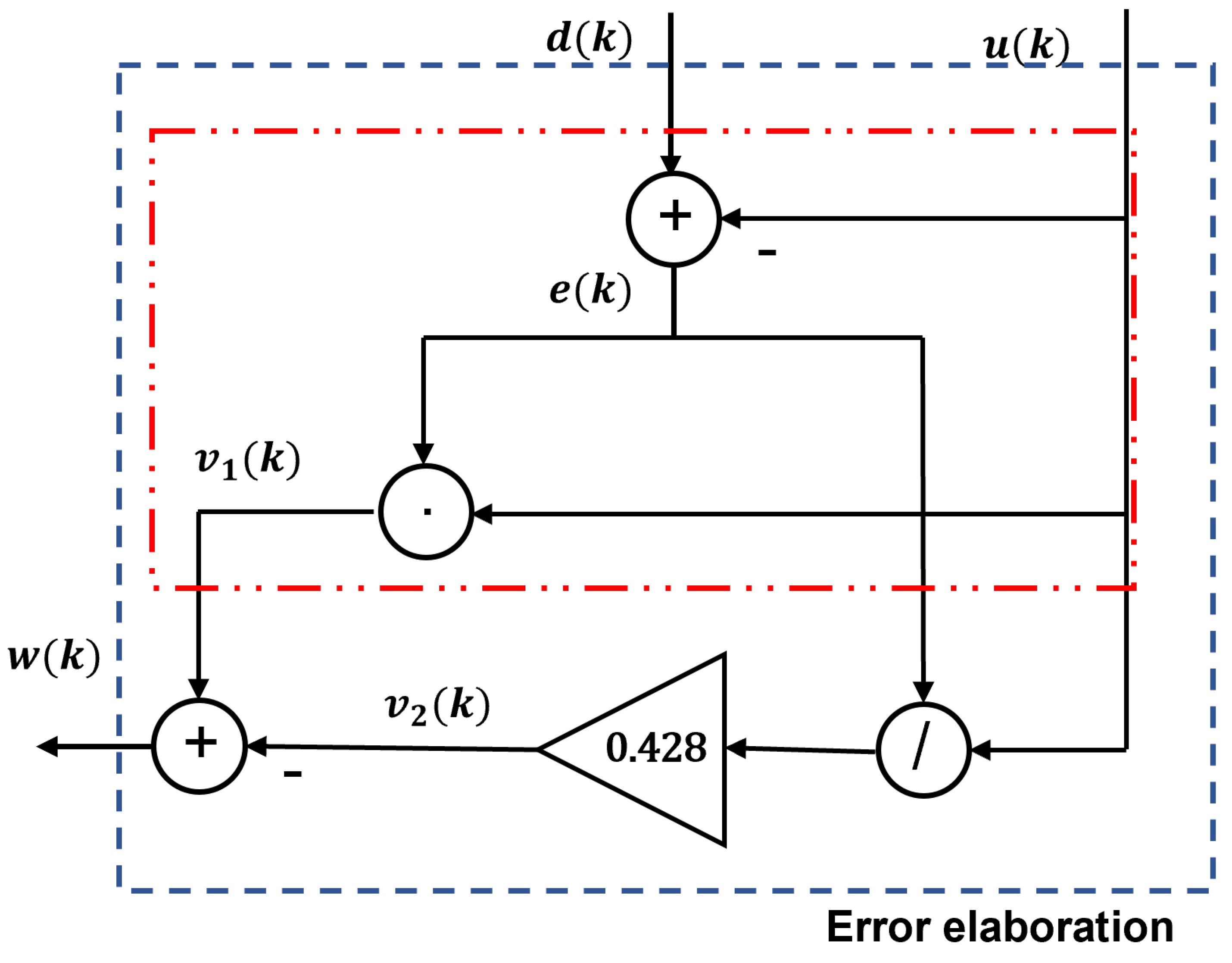
, which is not filtered, and which does not let the system settle to the desired value. To overcome these problems, we introduce the error elaboration block shown in Figure 6, different to the one in [8] allows us to remove not only the residual ISI component but also the gain error. For the simplicity of calculation, we assume a 3 is the only distortion component different from zero, d ( k ) is then:
d ( k ) = G r h e ( 1 ) u ( k ) + G n o r [ a 3 x 3 ( k ) + n ( k ) ] h F F E ( k ) ,
where G r is the residual gain of the system, which is different from 1, in the case when the system can not exactly match the gain of the channel (or the gain variations of the analog circuit components) G n o r 1 / G c h , and the first order terms given by the residual ISI are neglected because they will be filtered after being multiplied or divided by u ( k ) . Then, by following the calculation shown in the block diagram we have:
e ( k ) = [ G r h e ( 1 ) 1 ] u ( k ) + G n o r [ a 3 x 3 ( k ) + n ( k ) ] h F F E ( k )
v 1 ( k ) = [ G r h e ( 1 ) 1 ] u 2 ( k ) + u ( k ) G n o r [ a 3 x 3 ( k ) + n ( k ) ] h F F E ( k )
v 2 ( k ) = C E { [ G r h e ( 1 ) 1 ] + G n o r [ a 3 x 3 ( k ) + n ( k ) ] h F F E ( k ) / u ( k ) } .
Knowing that u ( k ) is a random signal, which can assume eight evenly spaced values between 1 and 1, we have C E = E u 2 ( k ) = 0.4286 , and after subtracting v 1 ( k ) v 2 ( k ) the filtering of the signal w ( k ) , we obtain:
v c o r r ( k ) 0.14 G a 3 C 3 G c h 2 .
This allows correct calculation of the system while being independent of the gain and the residual ISI. The error signal must be divided by one of the eight PAM-8 symbols. This means we can easily implement the division with a look-up table (LUT) to obtain the reciprocal of the symbol values followed by a multiplier. This can be performed with ease because the operation is carried on in the calibration path where the loop bandwidths can be small, and latency can be tolerated. Moreover, this elaboration block complexity does not change with the increasing ISI, while the one in [8] requires a number of delays and sums that scale quadratically with the number of nonnegligible ISI components. Therefore, in the presence of a channel difficult to equalize, the system presented in this work does not show criticality.
By operating on samples coming from different interleaving TH buffers and switches, the mismatches impact is averaged out. This means the loop will converge at a v c o r r that minimizes the overall distortions, but at the cost of a reduction in linearity compared to the ideal matching case.

4. Simulation Results

The validation of the feedback loop was performed by firstly implementing the track-and-hold circuit in TSMC 5 nm technology. During the simulation of the sampler, parasitics were added to the schematics. Principally, they were resistances and capacitances deriving from the post-layout characterization of the technology with the main focus on contact and low metal parasitics, which are critical.
While sampling the signal at 60 GS/s, the TH circuit had an output range of 505 mVppd generated through a 6 dB gain at Nyquist, and it consumed 18.5 mA from a 0.93 V voltage supply to drive the 64 TI channels capacitive loads equal to 45 fF. The ADC, the digital part of the PAM-8 RX, and the calibration loop were implemented in Verilog-A to enable co-simulation with the actual circuit. TX, AFE, and the channel were modeled using an s parameter matrix.
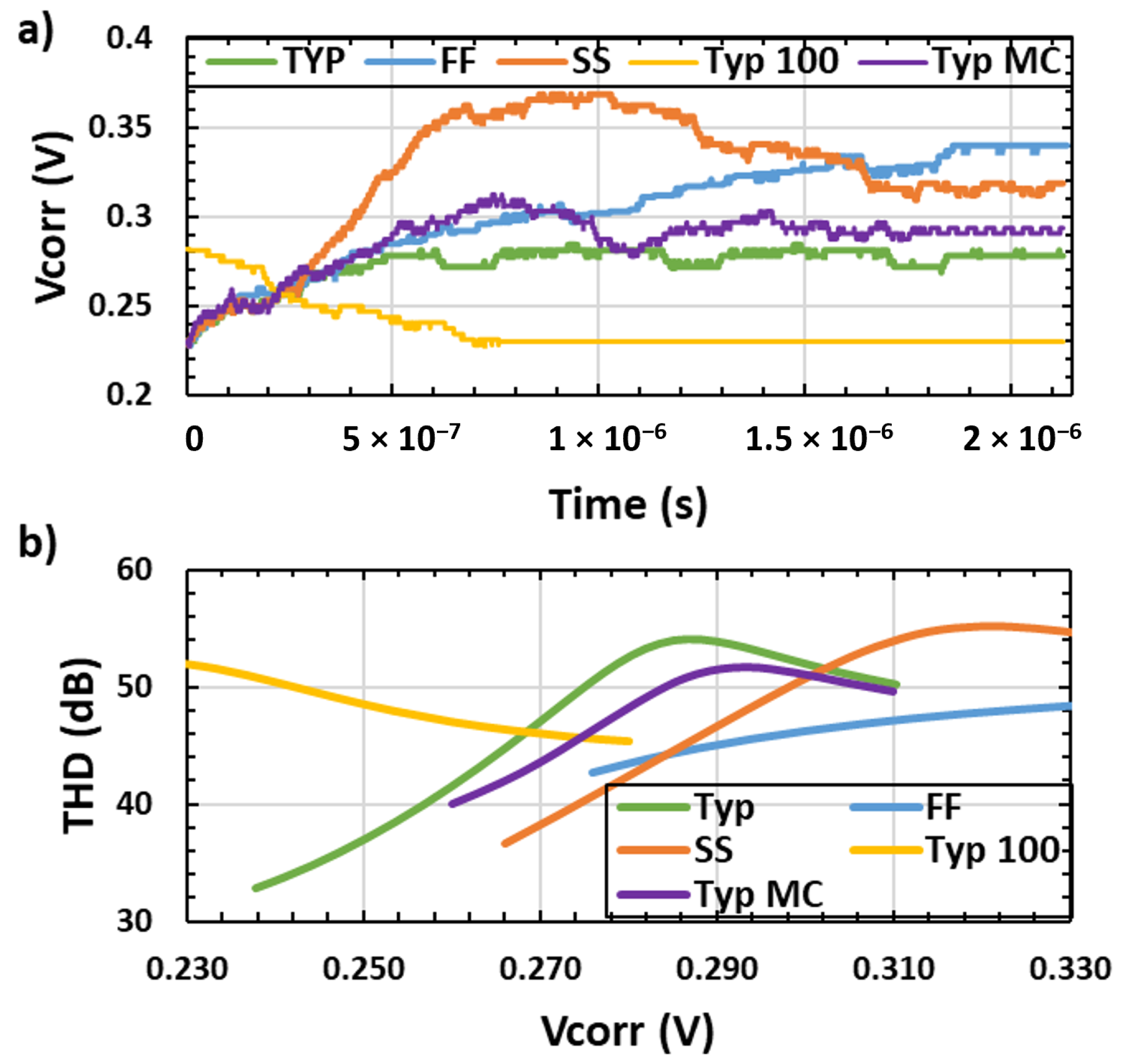
We performed a transient simulation of the receiver using a PRBS PAM-8 signal for three different PVT conditions. As shown in Figure 7a, the system adjusted the value of v c o r r over time until it settled to the optimal value (around 128 × 10 3 symbols against the 1.2 × 10 6 in [
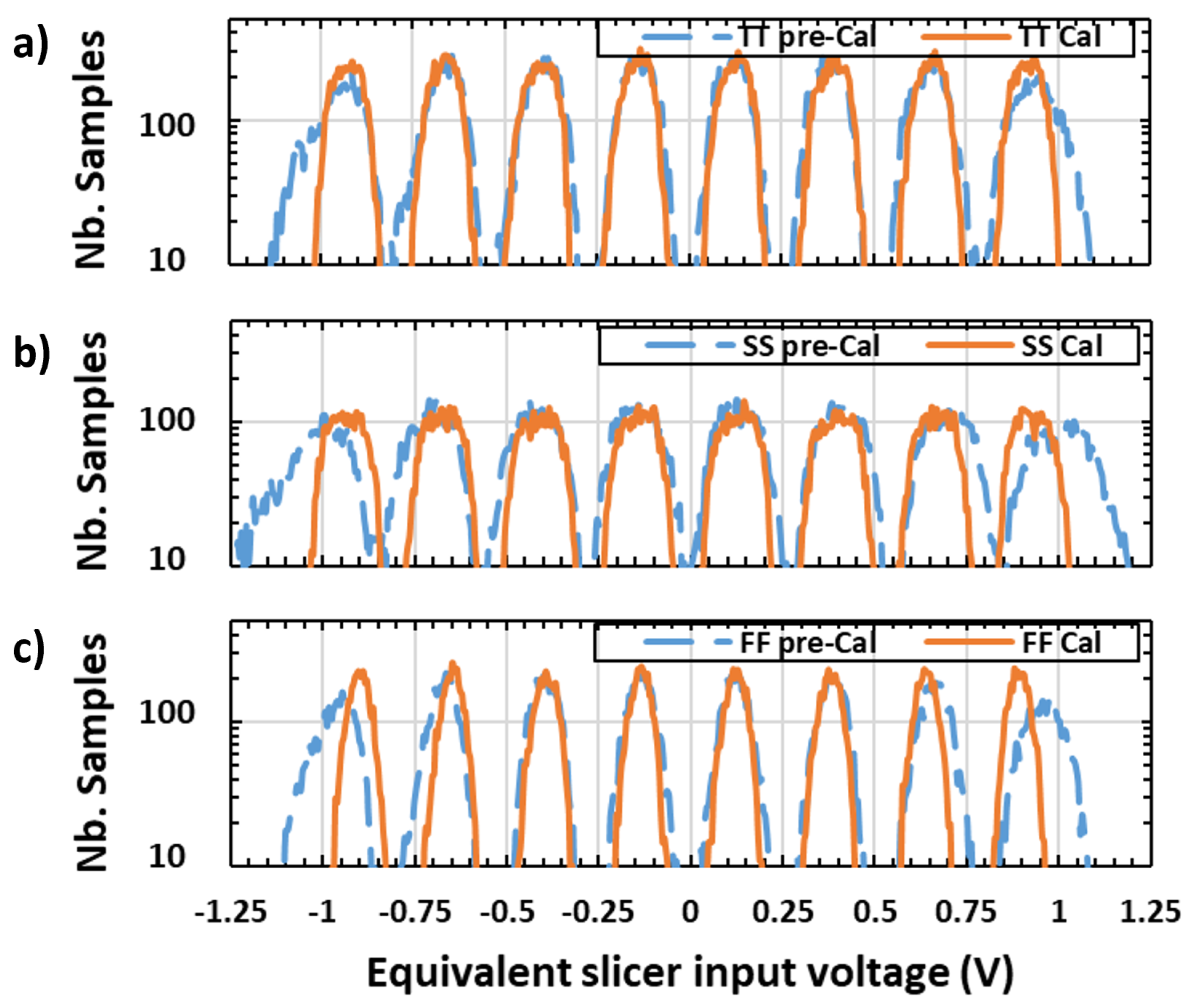
12]). By plotting in Figure 8 the histograms of the sampled signals equalized by the FFE at the beginning and the end of the calibration (the three couples of histograms are normalized so that the systems have the same linear gain in both cases), we can easily see an improvement. In particular, the average variance of the eight symbols moved from 34 mV to 27 mV, from 43 mV to 36 mV, and from 27 mV to 19 mV, respectively, for the Typ, SS, and FF corners. Next, the receiver was simulated using an input sinusoid of 252 mVppd at 1 GHz. 
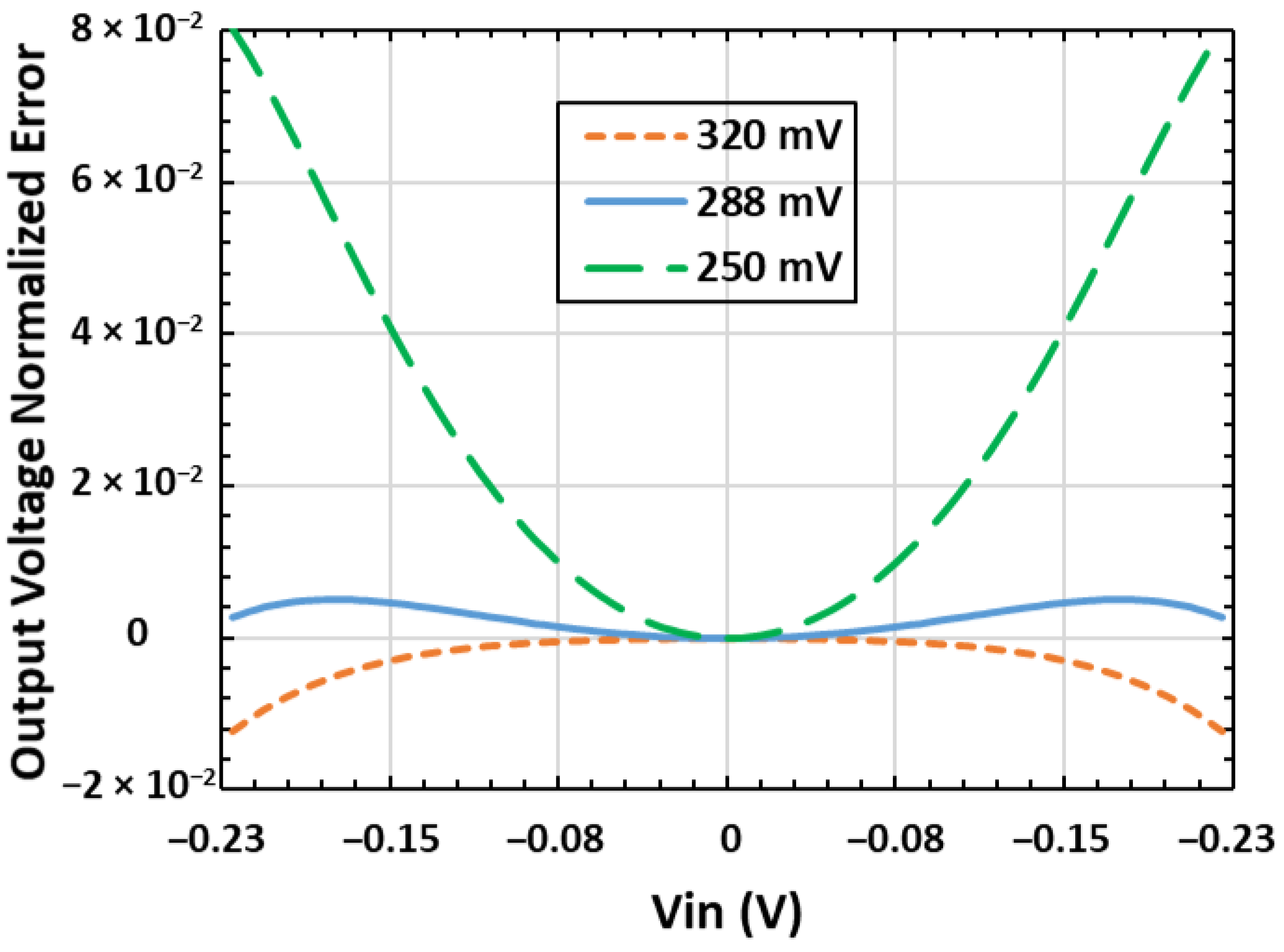
Figure 7b depicts the total harmonic distortion of the track and hold output signal with the varying of the v c o r r .
The maximum linearity of over 48.5 dB was obtained for values of v c o r r that matched the ones obtained through the transient calibration simulation, meaning that the system can maximize the static linearity. These simulations were also performed to obtain the plots in Figure 7 for a single Montecarlo (MC) point and after a temperature step. By looking at the MC results, we can see how the system set to a value that maximized the linearity while having lower linearity compared to the ideal case due to mismatches. The temperature tracking was verified by introducing a positive step (60 °C → 100 °C) after the v c o r r was settled in the Typical 60 °C condition (green case). The system set to the new value of v c o r r that maximized the linearity for 100 °C, meaning the system tracked the temperature variations, which were slower in real applications and presented less criticality. The sampled PAC simulation of the system with the varying of v c o r r was also performed, showing that the frequency response of the system had the same behavior (0.15% bandwidth variation), except for the gain as expected, which showed an 18% variation.
In Table 1, the THD of the circuit proposed in this work is compared with the available literature. A fair comparison is illustrated in [14] where a THD of around 50 dB was obtained for a the same input frequency and output dynamic range for a single PVT condition. On the other hand, in [12], the authors reported a THD of 56.5 dB after the calibration, but, to our knowledge, no throughout characterization of the analog circuit linearity across PVT nor co-simulation with the transistor-level circuit was performed.

5. Conclusions

This paper showed a 60 GS/s 8 × 8 TI track and hold in 5 nm FinFET technology with a 6 dB gain at Nyquist, and it proposed a calibration loop applicable to a PAM system, which minimized the distortion of the AFE. The transient co-simulation of the sampler circuit and of the receiver Verilog-A model generated the optimal value of v c o r r , and the system was able to vary the control voltage to track the temperature change. The histograms at the slicer were evaluated before and after the calibration showing an eye-opening improvement, which resulted in an average reduction in the variances from 34 mV to 27 mV, from 43 mV to 36 mV, and from 27 mV to 19 mV, respectively, for the Typ, SS, and FF corners. Lastly, the obtained v c o r r was applied to the buffer during a transient simulation with a 1 GHz, 252 m V p p d sinusoidal input, showing a THD of the TH circuit higher than 48.5 dB across different PVT conditions.

Author Contributions

Conceptualization, A.D.P., E.M. and N.G.; methodology, A.D.P., E.M., N.G. and C.N.; validation, A.D.P., E.M., N.G. and C.N.; formal analysis, A.D.P., E.M., N.G. and C.N.; investigation, A.D.P., E.M. and N.G.; data curation, A.D.P.; writing—original draft preparation, A.D.P.; writing—review and editing, A.D.P., E.M., N.G., C.N. and L.F.; supervision, C.N. and L.F. All authors have read and agreed to the published version of the manuscript.

Funding

This research received no external funding.

Data Availability Statement

Not applicable.

Conflicts of Interest

The authors declare no conflict of interest.

References

  1. Bailey, J.; Shakiba, H.; Nir, E.; Marderfeld, G.; Krotnev, P.; LaCroix, M.-A.; Cassan, D.; Tonietto, D. A 112-Gb/s PAM-4 Low-Power Nine-Tap Sliding-Block DFE in a 7-nm FinFET Wireline Receiver. IEEE J. Solid-State Circuits 2022, 57, 32–43. [Google Scholar] [CrossRef]
  2. Krupnik, Y.; Perelman, Y.; Levin, I.; Sanhedrai, Y.; Eitan, R.; Khairi, A.; Landau, Y.; Virobnik, U.; Dolev, N.; Meisler, A.; et al. 112 Gb/s PAM4 ADC Based SERDES Receiver for Long-Reach Channels in 10 nm Process. In Proceedings of the 2019 Symposium on VLSI Circuits, Kyoto, Japan, 9–14 June 2019; pp. C266–C267. [Google Scholar] [CrossRef]
  3. Pisati, M.; Minuti, A.; Bollati, G.; Giunco, F.; Massolini, R.G.; Cesura, G.; De Bernardinis, F.; Pascale, P.; Nani, C.; Ghittori, N.; et al. A 243-mW 1.25–56-Gb/s Continuous Range PAM-4 42.5-dB IL ADC/DAC-Based Transceiver in 7-nm FinFET. IEEE J. Solid-State Circuits 2012, 55, 6–18. [Google Scholar] [CrossRef]
  4. Foley, D.J.; Flynn, M.P. A low-power 8-PAM serial transceiver in 0.5-/spl mu/m digital CMOS. IEEE J. Solid-State Circuits 2002, 37, 310–316. [Google Scholar] [CrossRef]
  5. Chong, E.; Musa, F.A.; Mustafa, A.N.; Gao, T.; Krotnev, P.; Soreefan, R.; Xin, Q.; Madeira, P.; Tonietto, D. A 112Gb/s PAM-4, 168Gb/s PAM-8 7bit DAC-Based Transmitter in 7nm FinFET. In Proceedings of the ESSCIRC 2021—IEEE 47th European Solid State Circuits Conference (ESSCIRC), Grenoble, France, 13–22 September 2021; pp. 523–526. [Google Scholar] [CrossRef]
  6. Chun, Y.; Megahed, M.; Ramachandran, A.; Anand, T. A PAM-8 Wireline Transceiver With Linearity Improvement Technique and a Time-Domain Receiver Side FFE in 65 nm CMOS. IEEE J. Solid-State Circuits 2022, 57, 1527–1541. [Google Scholar] [CrossRef]
  7. Megahed, M.; Chun, Y.; Wang, Z.; Anand, T. A 27 Gb/s 5.39 pJ/bit 8-ary Modulated Wireline Transceiver Using Pulse Width and Amplitude Modulation Achieving 9.5 dB SNR Improvement over PAM-8. In Proceedings of the 2021 Symposium on VLSI Circuits, Kyoto, Japan, 13–19 June 2021; pp. 1–2. [Google Scholar] [CrossRef]
  8. Di Pasquo, A.; Monaco, E.; Ghittori, N.; Nani, C.; Fanucci, L. A Track-and-Hold Circuit with Tunable Non-Linearity and a Calibration Loop for PAM-8 SerDes Receivers. Electronics 2022, 11, 2199. [Google Scholar] [CrossRef]
  9. Li, J.; Wu, S.; Liu, Y.; Ning, N.; Yu, Q. A Digital Timing Mismatch Calibration Technique in Time-Interleaved ADCs. IEEE Trans. Circuits Syst. II Express Briefs 2014, 61, 486–490. [Google Scholar] [CrossRef]
  10. Hung, T.-C.; Liao, F.-W.; Kuo, T.-H. A 12-Bit Time-Interleaved 400-MS/s Pipelined ADC With Split-ADC Digital Background Calibration in 4,000 Conversions/Channel. IEEE Trans. Circuits Syst. II Express Briefs 2019, 66, 1810–1814. [Google Scholar] [CrossRef]
  11. Zhao, H.; Diaz, J.C.G.; Hoyos, S. Multi-Channel Receiver Nonlinearity Cancellation Using Channel Speculation Passing Algorithm. IEEE Trans. Circuits Syst. II Express Briefs 2022, 69, 599–603. [Google Scholar] [CrossRef]
  12. Bocco, A.F.; Solis, F.; Reyes, B.T.; Morero, D.A.; Hueda, M.R. Background Compensation of Static TI-ADC Nonlinearities in Coherent Optical Receivers. In Proceedings of the 2021 Argentine Conference on Electronics (CAE), Bahia Blanca, Argentina, 11–12 March 2021; pp. 45–49. [Google Scholar] [CrossRef]
  13. Di Pasquo, A.; Nani, C.; Monaco, E.; Fanucci, L. A High Linearity Driver with Embedded Interleaved Track-and-Hold Array for High-Speed ADC. In Proceedings of the 2021 IEEE International Symposium on Circuits and Systems (ISCAS), Daegu, Korea, 22–28 May 2021; pp. 1–5. [Google Scholar] [CrossRef]
  14. Mattia, E.O.; Murmann, B. 80 GS/s 5.5 ENOB time-interleaved inverter-based CMOS track-and-hold. Electron. Lett. 2020, 56, 328–329. [Google Scholar] [CrossRef]
  15. Zheng, K.; Frans, Y.; Ambatipudi, S.L.; Asuncion, S.; Reddy, H.T.; Chang, K.; Murmann, B. An Inverter-Based Analog Front-End for a 56-Gb/s PAM-4 Wireline Transceiver in 16-nm CMOS. IEEE Solid-State Circuits Letters. IEEE Solid-State Circuits Lett. 2019, 1, 249–252. [Google Scholar] [CrossRef]
  16. Luo, L.; Chen, S.; Zhou, M.; Ye, T. A 0.014mm2 10-bit 2GS/s time-interleaved SAR ADC with low-complexity background timing skew calibration. In Proceedings of the 2017 Symposium on VLSI Circuits, Kyoto, Japan, 5–8 June 2017; pp. C278–C279. [Google Scholar] [CrossRef]
Figure 1. (a) MSE and (b) SER with the varying of SNR for various THD [8].
Electronics 11 03484 g001
Figure 2. Block diagram of a 64 TI-TH circuit with in blue the first stage sampler and in green the second state, using a DAC for the second-stage buffer bias voltage control [8].
Electronics 11 03484 g002
Figure 3. Second-stage TH buffer in blue with its distortion contribution compensating for the previous stages non-linear block in green [8].
Electronics 11 03484 g003
Figure 4. The ϵ r with the varying of the large-signal differential input for various bias voltages v c o r r [8].
Electronics 11 03484 g004
Figure 5. PAM-8 RX using the calibration loop with the transistor level components in blue and the Verilog-A model in green.
Electronics 11 03484 g005
Figure 6. The block that processes the difference between the input and the output of the slicer allowing cancellation of the residual ISI and gain error in blue (in red the non-robust to ISI and gain elaboration block).
Electronics 11 03484 g006
Figure 7. (a) Settling of the v c o r r overtime during the calibration of the system and (b) the THD of the TH circuit across different values of v c o r r for three different PVT conditions, one MC point, and one after a temperature step (the plot stops at v c o r r = 0.33 V due to the linearity saturation (FF) for higher values).
Electronics 11 03484 g007
Figure 8. Histograms of the reconstructed signals at the slicer input before and after the linearity calibration for (a) Typical, (b) SS, and (c) FF corner.
Electronics 11 03484 g008
Table 1. THD comparison between the literature and this work at three different PVT conditions.
System[14]
Typ
[12]This Work
Typ @ 60 °C
This Work
SS @ 125 °C
This Work
FF @ −20 °C
Pre-calibration
THD
≈50 dB (No calibration was implemented; the THD was extrapolated from the plot)30.8 dB31.6 dB36.4 dB28.7 dB
Post-calibration
THD
-56.5 dB54.0 dB55.2 dB48.5 dB
Input
Frequency
1.01 GHz5.5 GHz1 GHz1 GHz1 GHz
Transistor-level
implementation
YesNoYesYesYes
Output
Dynamic Range
500 mVppd-500 mVppd500 mVppd500 mVppd
Publisher’s Note: MDPI stays neutral with regard to jurisdictional claims in published maps and institutional affiliations.

