
Simulation of TSV Protrusion in 3DIC Integration by Directly Loading on Coarse-Grained Phase-Field Crystal Model


 , , , ,
Abstract
:
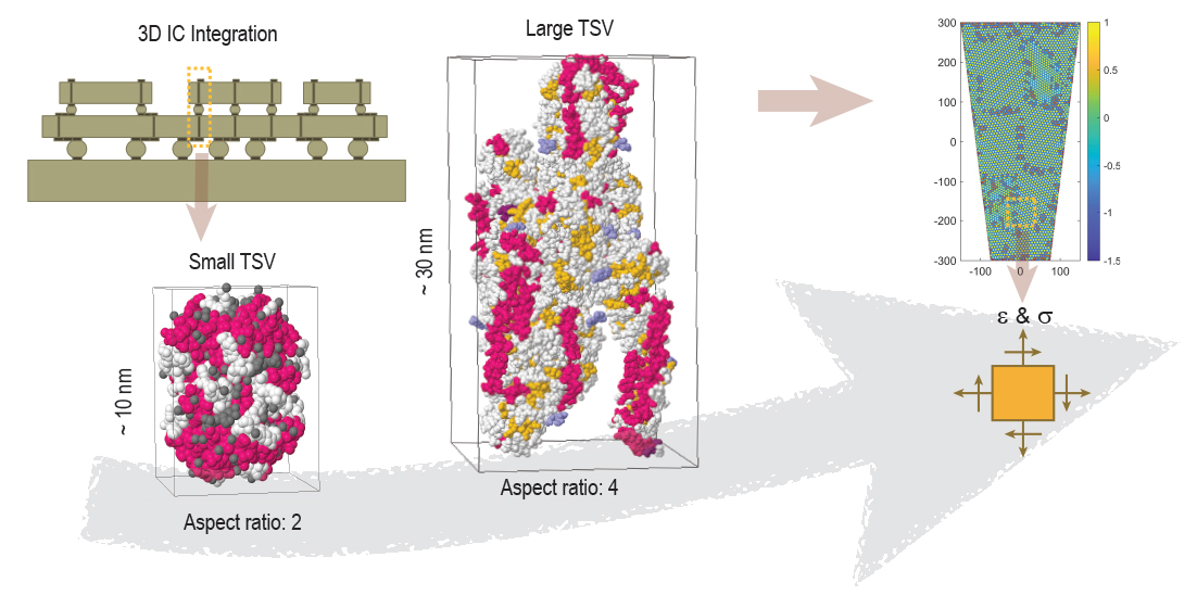
1. Introduction
2. Modeling Methods
2.1. The APFC Model
2.2. Initial Condition
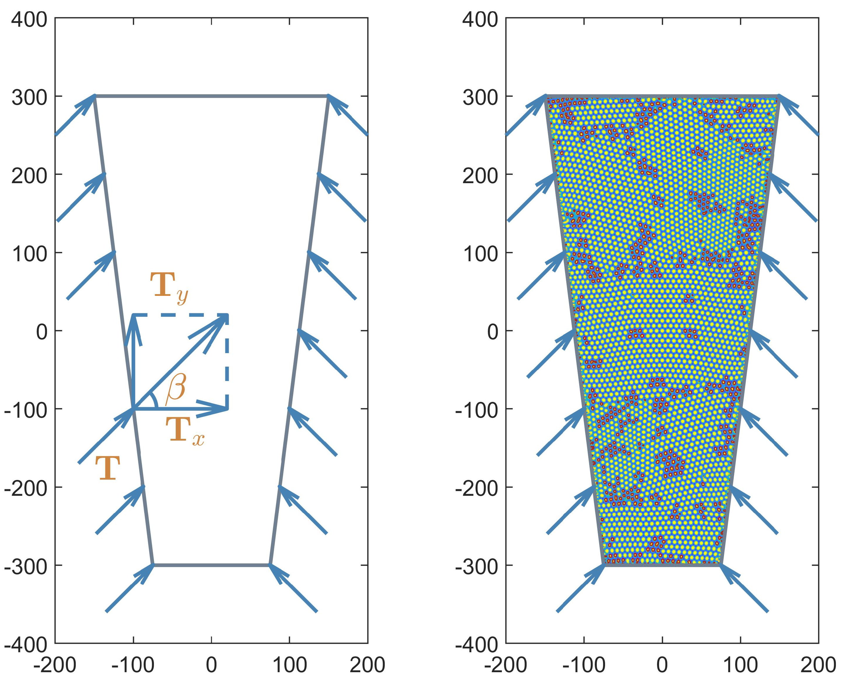
2.3. Deformation and Boundary Condition
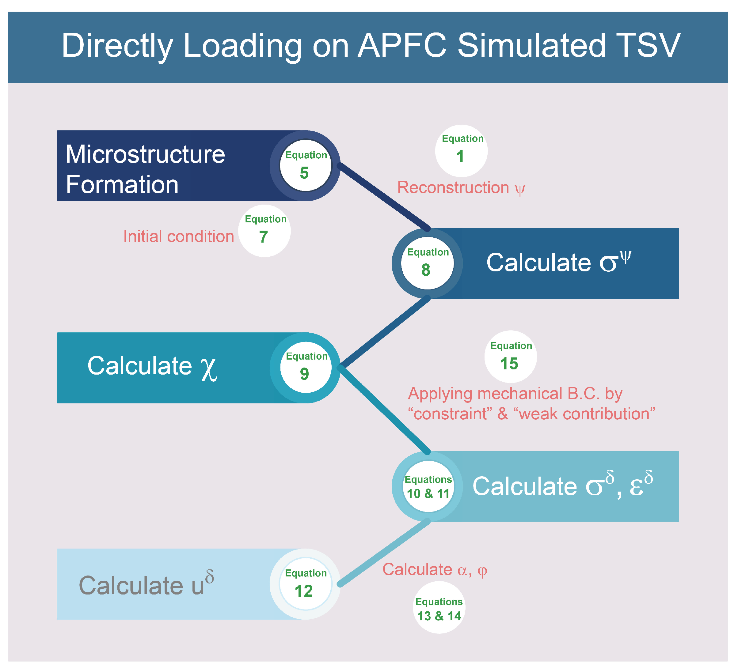
2.4. Model Implementation
3. Results and Discussion
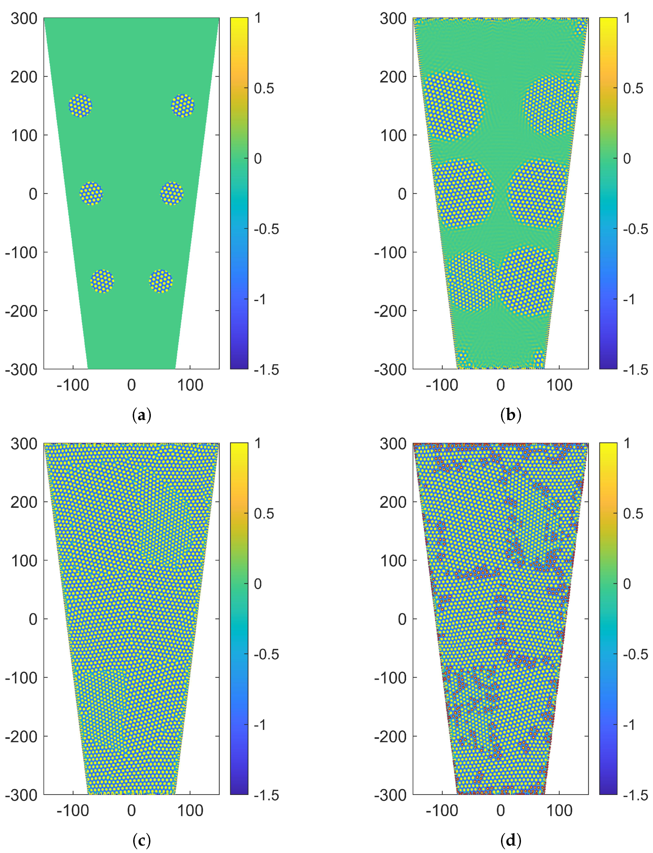
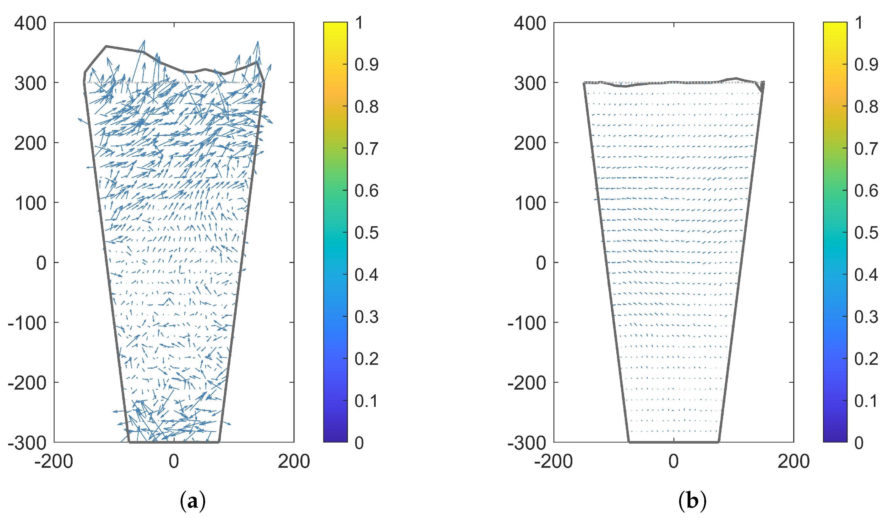
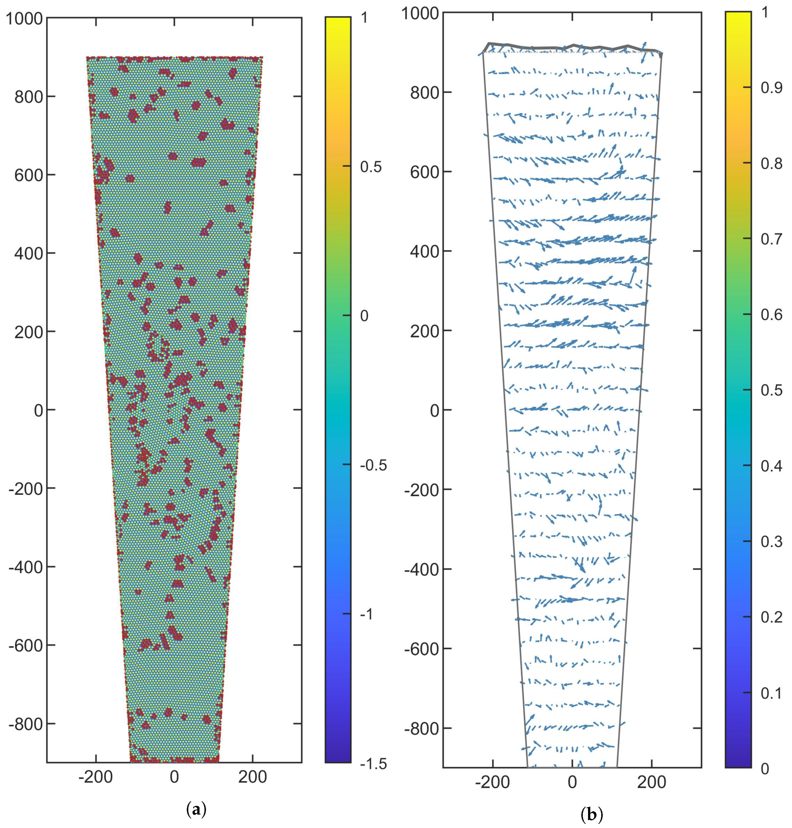
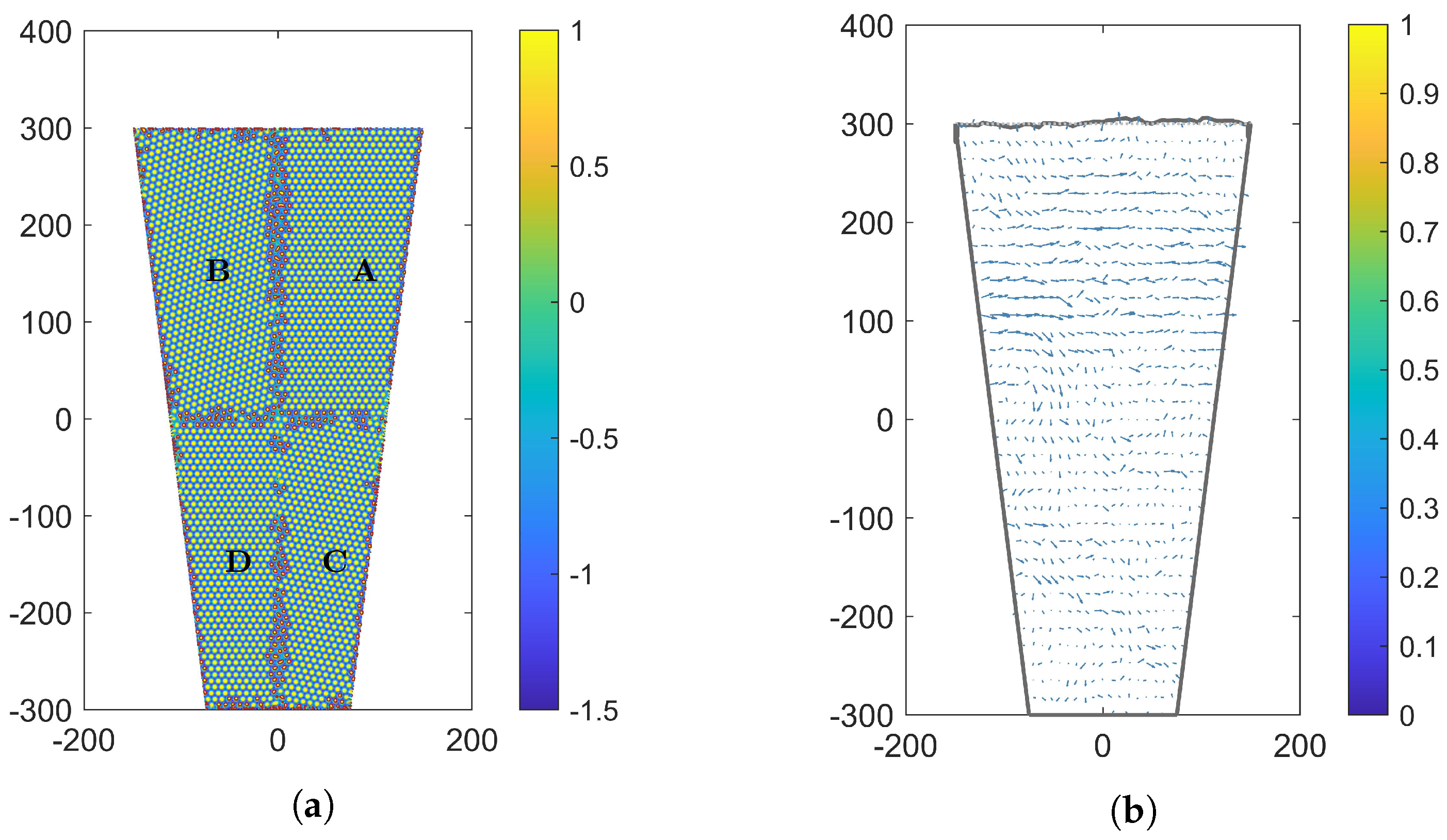
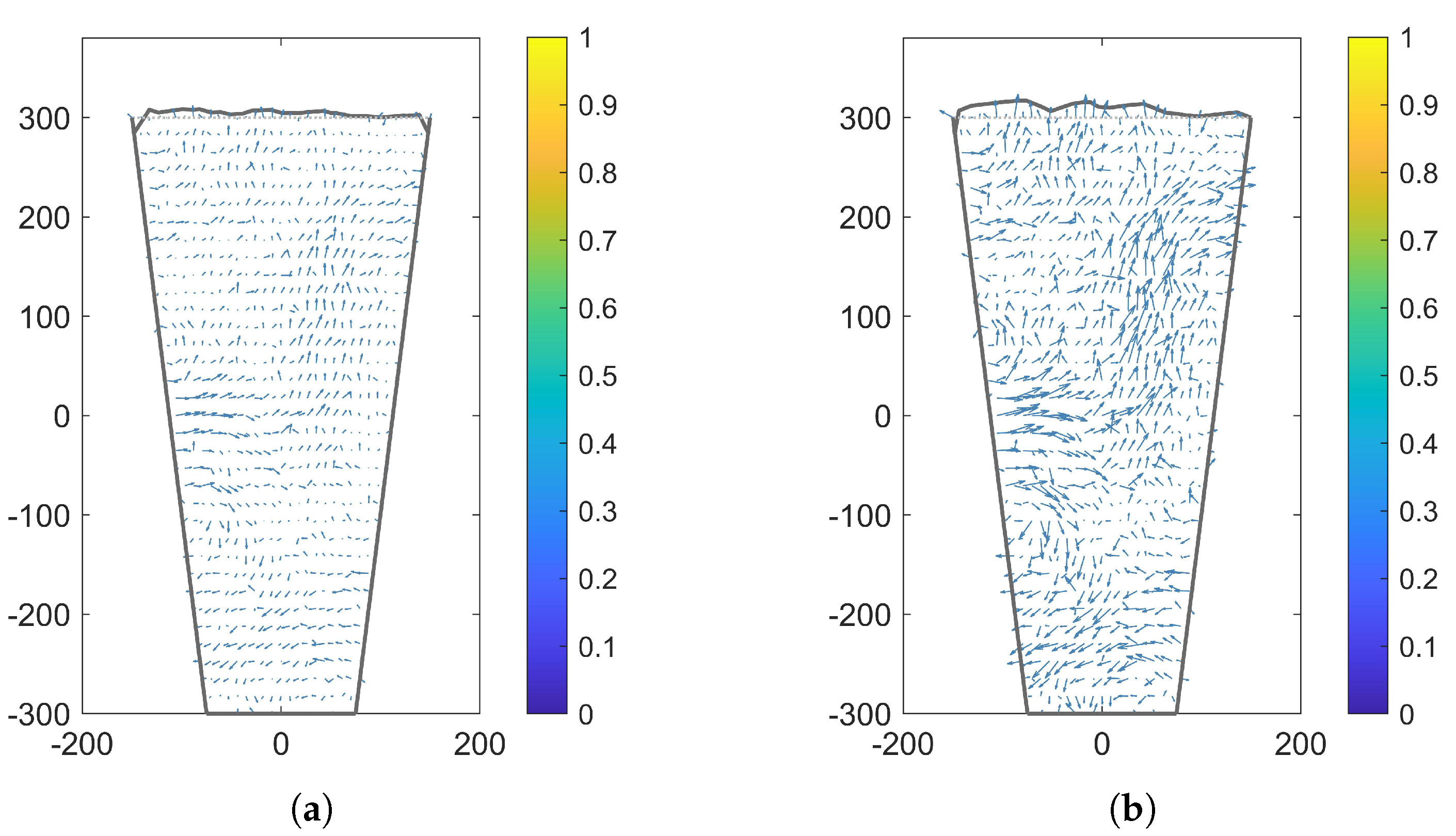
3.1. Microstructure Formation in TSV
3.2. Effect of Microstructure
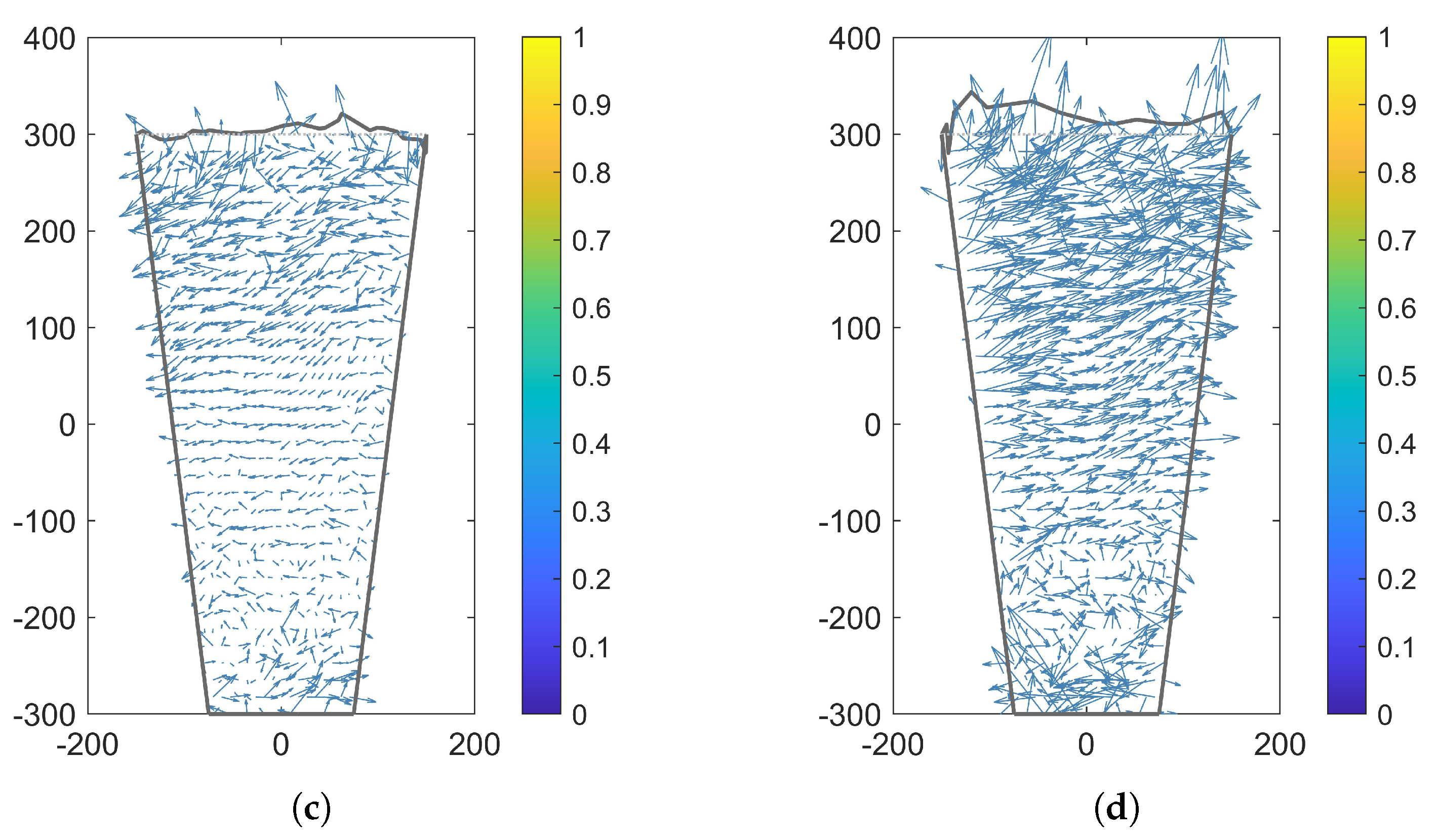
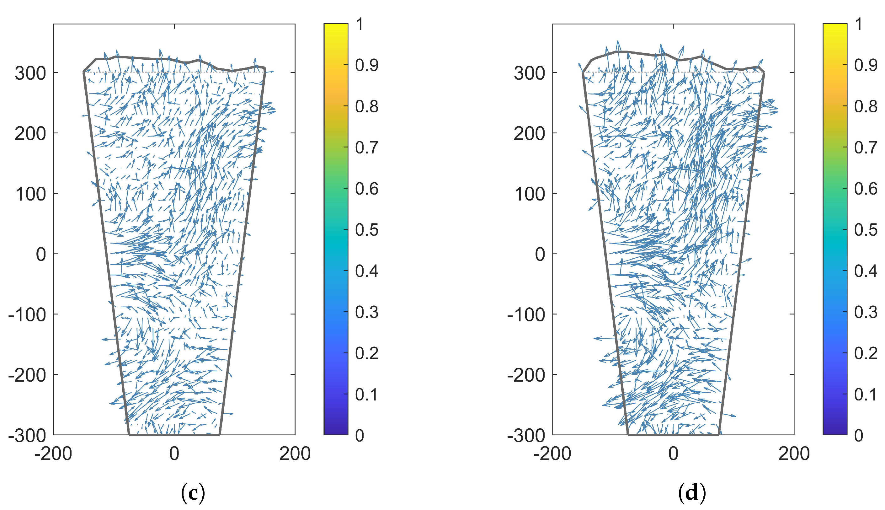
3.3. Effect of External Loading
4. Conclusions
Author Contributions
Funding
Data Availability Statement
Conflicts of Interest
References
- Moore, G.E. Cramming more components onto integrated circuits. Proc. IEEE 1998, 86, 82–85. [Google Scholar]
- Predicting Reliability at 3/2 nm and Beyond. Available online: https://semiengineering.com/predicting-reliability-at-3-2nm-and-beyond (accessed on 3 December 2021).
- Roth, A.; Zhou, C.; Wong, M.; Soenen, E.; Huang, T.C.; Ranucci, P.; Hsu, Y.C.; Lin, H.C.; Kuo, C.; Wang, M.J.; et al. Heterogeneous Power Delivery for 7 nm High-Performance Chiplet-Based Processors using Integrated Passive Device and In-Package Voltage Regulator. In Proceedings of the 2020 IEEE Symposium on VLSI Technology, Honolulu, HI, USA, 16–19 June 2020; pp. 1–2. [Google Scholar] [CrossRef]
- Ingerly, D.; Amin, S.; Aryasomayajula, L.; Balankutty, A.; Borst, D.; Chandra, A.; Cheemalapati, K.; Cook, C.; Criss, R.; Enamul, K.; et al. Foveros: 3D integration and the use of face-to-face chip stacking for logic devices. In Proceedings of the 2019 IEEE International Electron Devices Meeting (IEDM), San Francisco, CA, USA, 7–11 December 2019; IEEE: Piscataway, NJ, USA, 2019; pp. 19.6.1–19.6.4. [Google Scholar]
- Shen, X.; Xia, Z.; Yang, T.; Liu, L.; Dong, J.; Zhou, W.; Li, C.; Huo, Z. Hydrogen source and diffusion path for Poly-Si channel passivation in Xtacking 3D NAND flash memory. IEEE J. Electron. Devices Soc. 2020, 8, 1021–1024. [Google Scholar]
- Venkatadri, V.; Sammakia, B.; Srihari, K.; Santos, D. A review of recent advances in thermal management in three dimensional chip stacks in electronic systems. J. Electron. Packag. 2011, 133, 041011. [Google Scholar]
- Kandlikar, S.G. Review and projections of integrated cooling systems for three-dimensional integrated circuits. J. Electron. Packag. 2014, 136, 024001. [Google Scholar]
- Xiao, H. Introduction to Semiconductor Manufacturing Technology, 2nd ed.; SPIE: Bellingham, WA, USA, 2012. [Google Scholar]
- Lau, J.H. Heterogeneous Integrations, 1st ed.; Springer: Singapore, 2019. [Google Scholar]
- Okoro, C.; Levine, L.E.; Xu, R.; Obeng, Y.S. Experimentally, how does Cu TSV diameter influence its stress state? In Proceedings of the 2015 IEEE 65th Electronic Components and Technology Conference (ECTC), San Diego, CA, USA, 26–29 May 2015; IEEE: Piscataway, NJ, USA, 2015; pp. 54–58. [Google Scholar]
- Jung, M.; Pan, D.Z.; Lim, S.K. Through-silicon-via material property variation impact on full-chip reliability and timing. In Proceedings of the IEEE International Interconnect Technology Conference, San Jose, CA, USA, 20–23 May 2014; IEEE: Piscataway, NJ, USA, 2014; pp. 105–108. [Google Scholar]
- Sukharev, V.; Kteyan, A.; Choy, J.H. An Accurate Assessment of Chip-Package Interaction is a Key Factor for Designing Resilient 3D IC Systems. In Proceedings of the 2019 International 3D Systems Integration Conference (3DIC), Sendai, Japan, 8–10 October 2019; IEEE: Piscataway, NJ, USA, 2019; pp. 1–6. [Google Scholar]
- Liang, S.; Ke, C.; Wei, C.; Zhou, M.; Zhang, X. Study of the Influence of Elastic Anisotropy of Cu on Thermo-Mechanical Behavior and Cu Protrusion of Through Silicon Vias Using Combined Phase Field and Finite Element Methods. IEEE Trans. Device Mater. Reliab. 2019, 19, 322–332. [Google Scholar]
- Zhao, X.; Ma, L.; Wang, Y.; Guo, F. Mechanism of the local Cu protrusion in Cu-filled through silicon vias under heat treatment. J. Electron. Mater. 2019, 48, 152–158. [Google Scholar]
- Zhao, X.; Ma, L.; Wang, Y.; Guo, F. Effects of twin boundaries on the void formation in Cu-filled through silicon vias under thermal process. J. Mater. Sci. Mater. Electron. 2019, 30, 5845–5853. [Google Scholar]
- Jalilvand, G.; Ahmed, O.; Dube, N.; Jiang, T. The effect of pitch distance on the statistics and morphology of through-silicon via extrusion. IEEE Trans. Components Packag. Manuf. Technol. 2021, 11, 883–891. [Google Scholar]
- Ji, L.; Che, F.; Ji, H.; Li, H.; Kawano, M. Modelling and characterization on wafer to wafer hybrid bonding technology for 3D IC packaging. In Proceedings of the 2019 IEEE 21st Electronics Packaging Technology Conference (EPTC), Singapore, 4–6 December 2019; IEEE: Piscataway, NJ, USA, 2019; pp. 87–94. [Google Scholar]
- Ji, L.; Che, F.X.; Ji, H.M.; Li, H.Y.; Kawano, M. Wafer-to-Wafer Hybrid Bonding Development by Advanced Finite Element Modeling for 3-D IC Packages. IEEE Trans. Components Packag. Manuf. Technol. 2020, 10, 2106–2117. [Google Scholar]
- Liu, J.; Huang, Z.; Conway, P.P.; Liu, Y. Microstructural evolution and protrusion simulations of Cu-TSVs under different loading conditions. J. Electron. Packag. 2020, 142, 011009. [Google Scholar]
- Liu, J.; Huang, Z.; Zhang, Y.; Conway, P.P. Mechanisms of copper protrusion in through-silicon-via structures at the nanoscale. Jpn. J. Appl. Phys. 2018, 58, 016502. [Google Scholar]
- Jalilvand, G.; Lindsay, J.; Reidy, B.; Shukla, V.; Duggan, D.; Zand, R.; Jiang, T. Application of Machine Learning in Recognition and Analysis of TSV Extrusion Profiles with Multiple Morphology. In Proceedings of the 2021 IEEE 71st Electronic Components and Technology Conference (ECTC), San Diego, CA, USA, 1 June–4 July 2021; IEEE: Piscataway, NJ, USA, 2021; pp. 1652–1659. [Google Scholar]
- Goldenfeld, N.; Athreya, B.P.; Dantzig, J.A. Renormalization group approach to multiscale simulation of polycrystalline materials using the phase field crystal model. Phys. Rev. E 2005, 72, 020601. [Google Scholar]
- Goldenfeld, N.; Athreya, B.P.; Dantzig, J.A. Renormalization group approach to multiscale modelling in materials science. J. Stat. Phys. 2006, 125, 1015–1023. [Google Scholar]
- Skaugen, A.; Angheluta, L.; Viñals, J. Dislocation dynamics and crystal plasticity in the phase-field crystal model. Phys. Rev. B 2018, 97, 054113. [Google Scholar]
- Skaugen, A.; Angheluta, L.; Viñals, J. Separation of elastic and plastic timescales in a phase field crystal model. Phys. Rev. Lett. 2018, 121, 255501. [Google Scholar]
- Salvalaglio, M.; Angheluta, L.; Huang, Z.F.; Voigt, A.; Elder, K.R.; Viñals, J. A coarse-grained phase-field crystal model of plastic motion. J. Mech. Phys. Solids 2020, 137, 103856. [Google Scholar]
- Elder, K.; Katakowski, M.; Haataja, M.; Grant, M. Modeling elasticity in crystal growth. Phys. Rev. Lett. 2002, 88, 245701. [Google Scholar]
- Elder, K.; Grant, M. Modeling elastic and plastic deformations in nonequilibrium processing using phase field crystals. Phys. Rev. E 2004, 70, 051605. [Google Scholar]
- Salvalaglio, M.; Backofen, R.; Elder, K.; Voigt, A. Defects at grain boundaries: A coarse-grained, three-dimensional description by the amplitude expansion of the phase-field crystal model. Phys. Rev. Mater. 2018, 2, 053804. [Google Scholar]
- Salvalaglio, M.; Voigt, A.; Elder, K.R. Closing the gap between atomic-scale lattice deformations and continuum elasticity. Npj Comput. Mater. 2019, 5, 1–9. [Google Scholar]
- Salvalaglio, M.; Voigt, A.; Huang, Z.F.; Elder, K.R. Mesoscale Defect Motion in Binary Systems: Effects of Compositional Strain and Cottrell Atmospheres. Phys. Rev. Lett. 2021, 126, 185502. [Google Scholar]
- Salvalaglio, M.; Backofen, R.; Voigt, A.; Elder, K.R. Controlling the energy of defects and interfaces in the amplitude expansion of the phase-field crystal model. Phys. Rev. E 2017, 96, 023301. [Google Scholar]
- Spiesshoefer, S.; Rahman, Z.; Vangara, G.; Polamreddy, S.; Burkett, S.; Schaper, L. Process integration for through-silicon vias. J. Vac. Sci. Technol. A Vac. Surfaces Film. 2005, 23, 824–829. [Google Scholar]
- Hieckmann, E.; Mühle, U.; Chekhonin, P.; Zschech, E.; Gambino, J. Investigations of internal stresses in high-voltage devices with deep trenches. J. Vac. Sci. Technol. B, Nanotechnol. Microelectron. Mater. Process. Meas. Phenom. 2020, 38, 064004. [Google Scholar]
- Specifying Boundary Conditions and Constraints in Variational Problems. Available online: www.comsol.com/blogs/specifying-boundary-conditions-and-constraints-in-variational-problems (accessed on 3 December 2021).
- Yeap, K.B.; Roellig, M.; Huebner, R.; Gall, M.; Sukharev, V.; Zschech, E. A critical review on multiscale material database requirement for accurate three-dimensional IC simulation input. IEEE Trans. Device Mater. Reliab. 2012, 12, 217–224. [Google Scholar]
- Gottstein, G.; Shvindlerman, L.S. Grain Boundary Migration in Metals: Thermodynamics, Kinetics, Applications, 2nd ed.; CRC Press: Boca Raton, FL, USA, 2009. [Google Scholar]


Publisher’s Note: MDPI stays neutral with regard to jurisdictional claims in published maps and institutional affiliations. |
© 2022 by the authors. Licensee MDPI, Basel, Switzerland. This article is an open access article distributed under the terms and conditions of the Creative Commons Attribution (CC BY) license (https://creativecommons.org/licenses/by/4.0/).
Share and Cite
Luo, X.; Huang, Z.; Wang, S.; Xiao, M.; Meng, Y.; Yan, H.; Li, Q.; Wang, G. Simulation of TSV Protrusion in 3DIC Integration by Directly Loading on Coarse-Grained Phase-Field Crystal Model. Electronics 2022, 11, 221. https://doi.org/10.3390/electronics11020221
Luo X, Huang Z, Wang S, Xiao M, Meng Y, Yan H, Li Q, Wang G. Simulation of TSV Protrusion in 3DIC Integration by Directly Loading on Coarse-Grained Phase-Field Crystal Model. Electronics. 2022; 11(2):221. https://doi.org/10.3390/electronics11020221
Chicago/Turabian StyleLuo, Xiaoting, Zhiheng Huang, Shuanjin Wang, Min Xiao, Yuezhong Meng, Hui Yan, Qizhuo Li, and Gang Wang. 2022. "Simulation of TSV Protrusion in 3DIC Integration by Directly Loading on Coarse-Grained Phase-Field Crystal Model" Electronics 11, no. 2: 221. https://doi.org/10.3390/electronics11020221