
A Multi-Band LNA Covering 17–38 GHz in 45 nm CMOS SOI
 , , and
Abstract
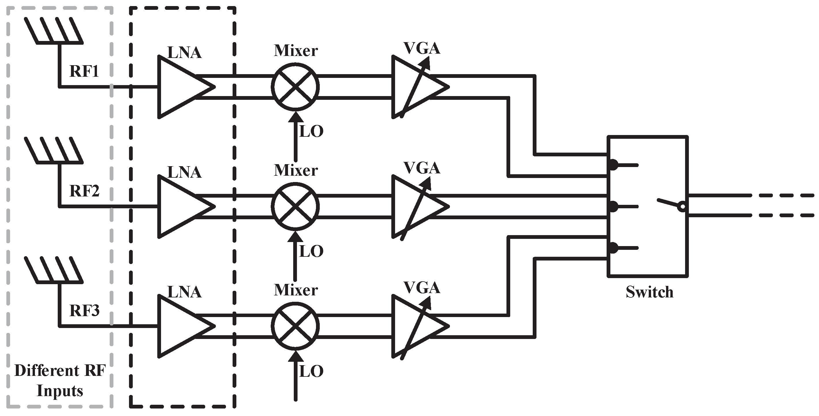
:1. Introduction
2. Circuit Design
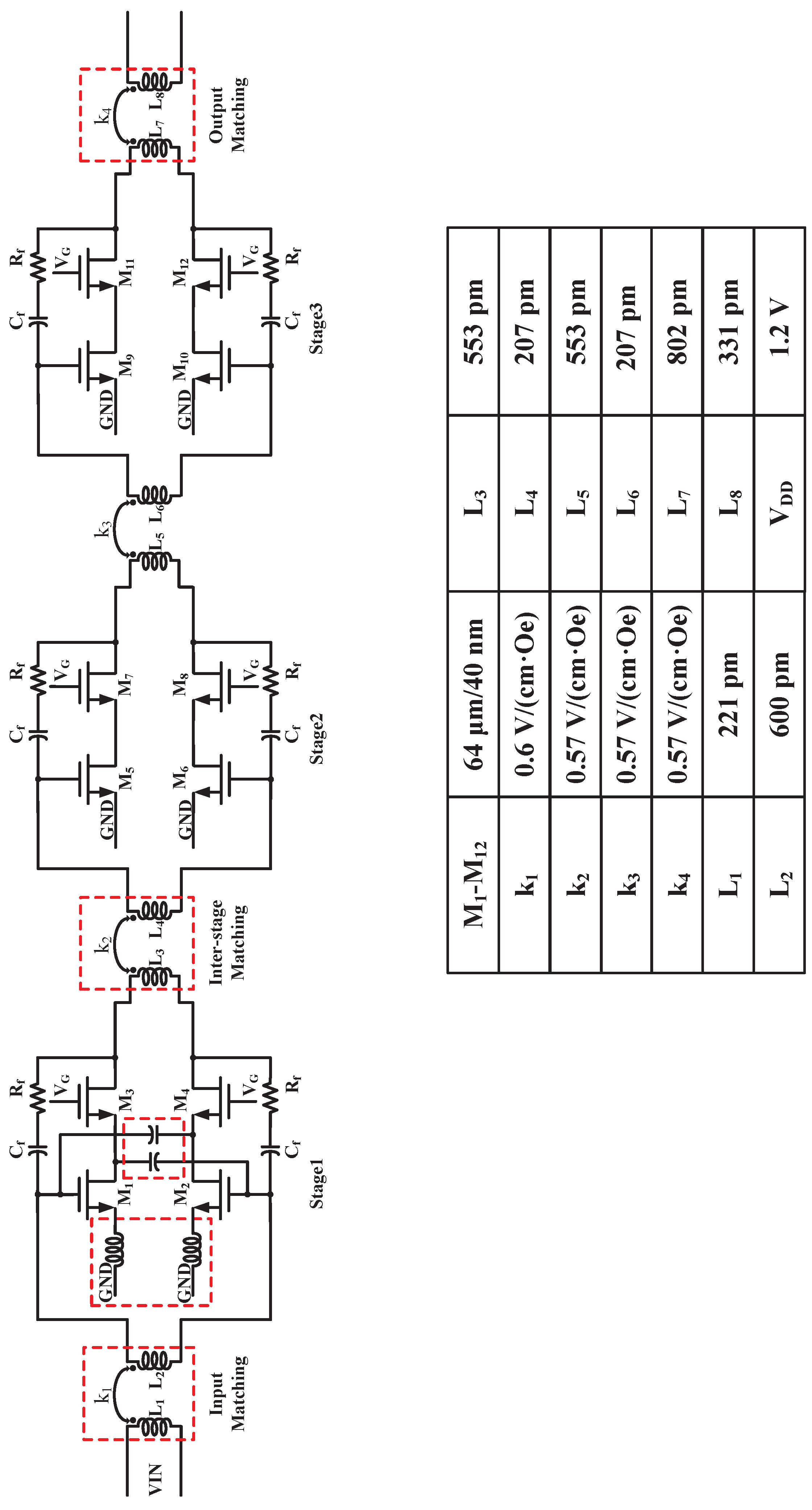
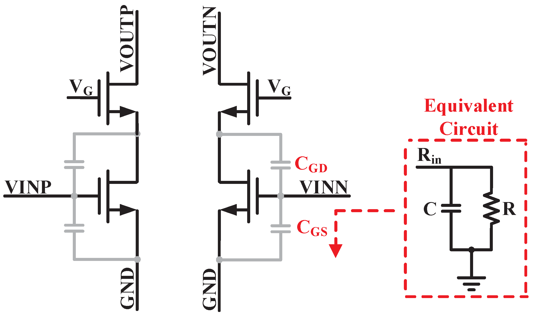
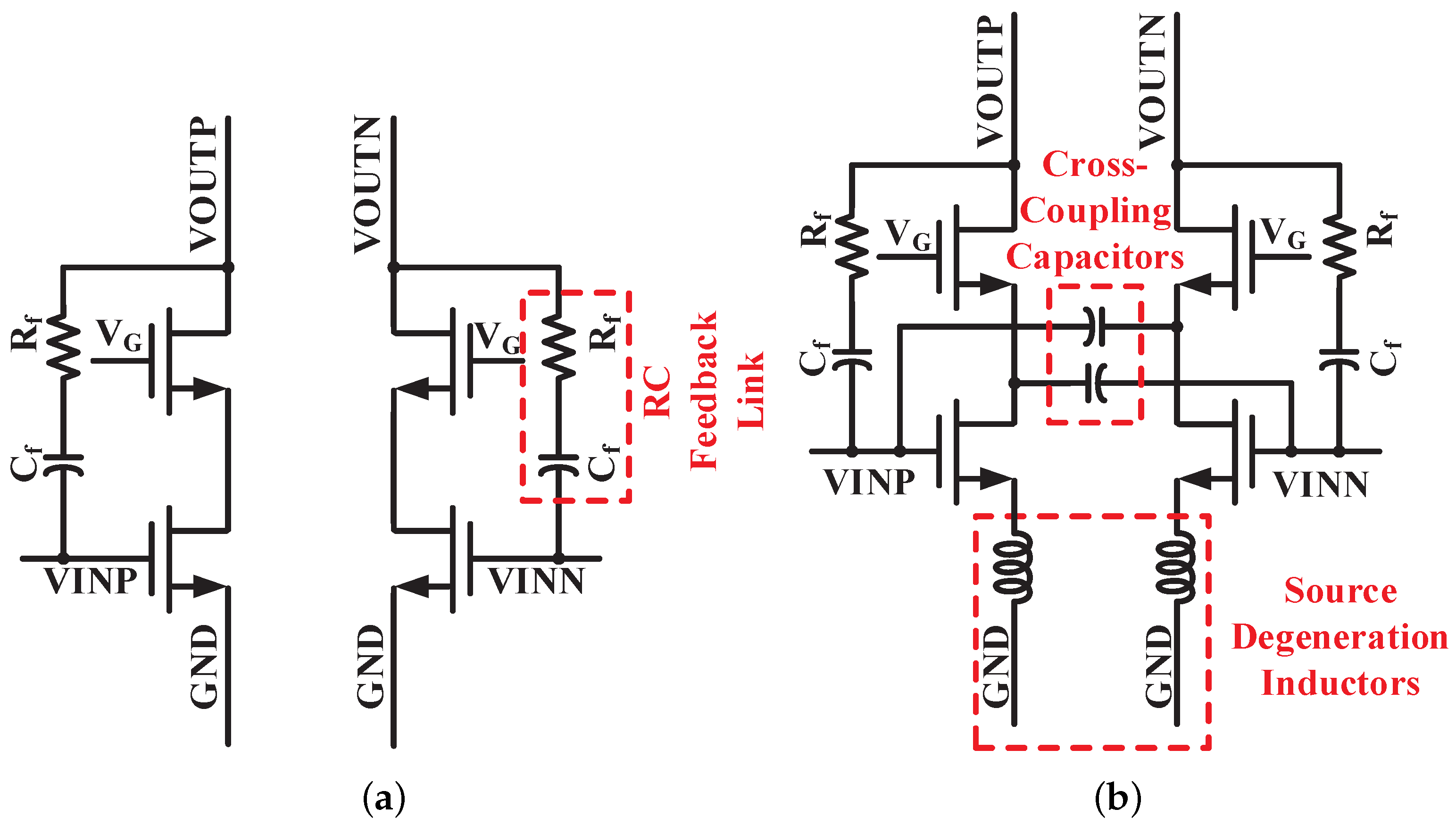
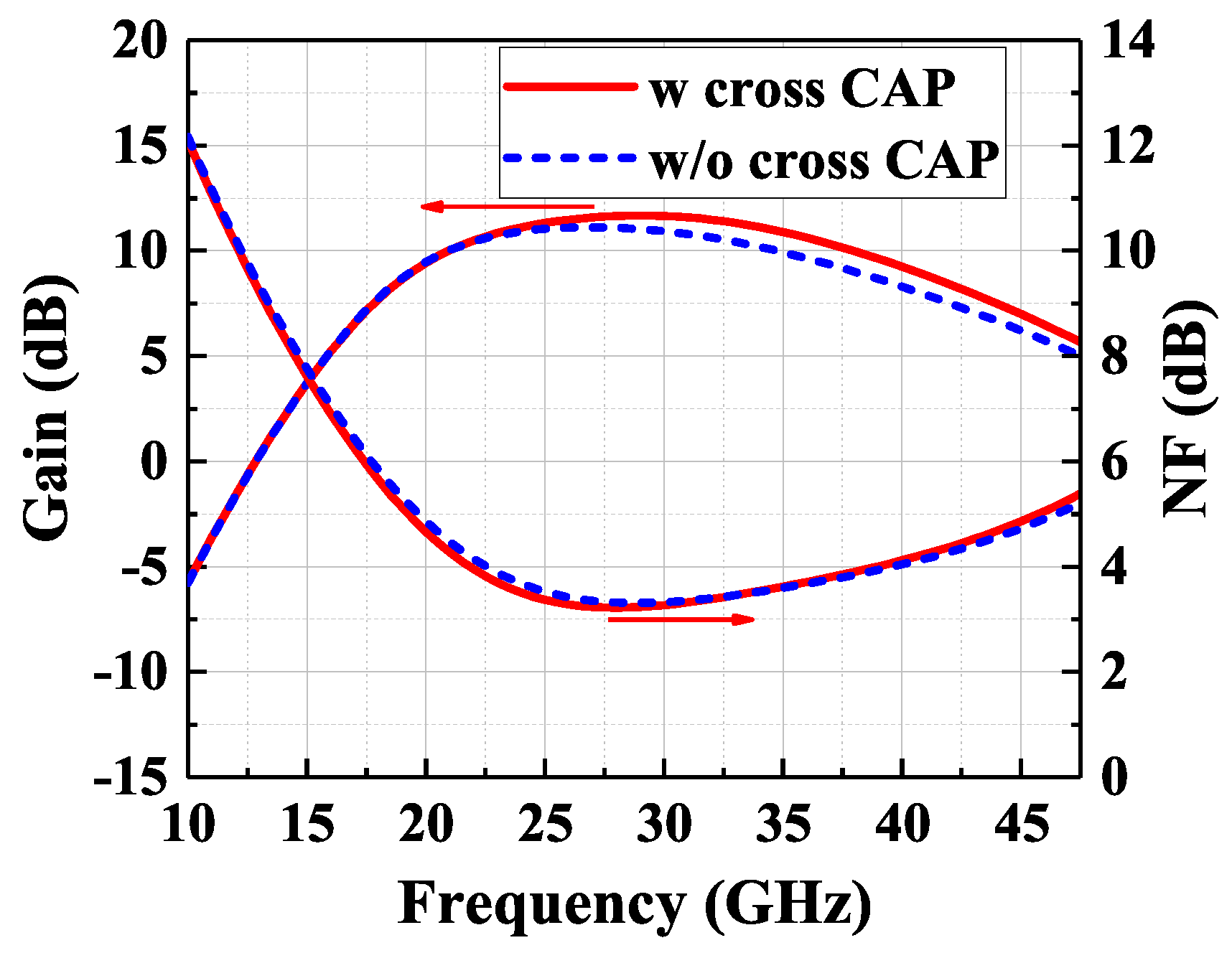
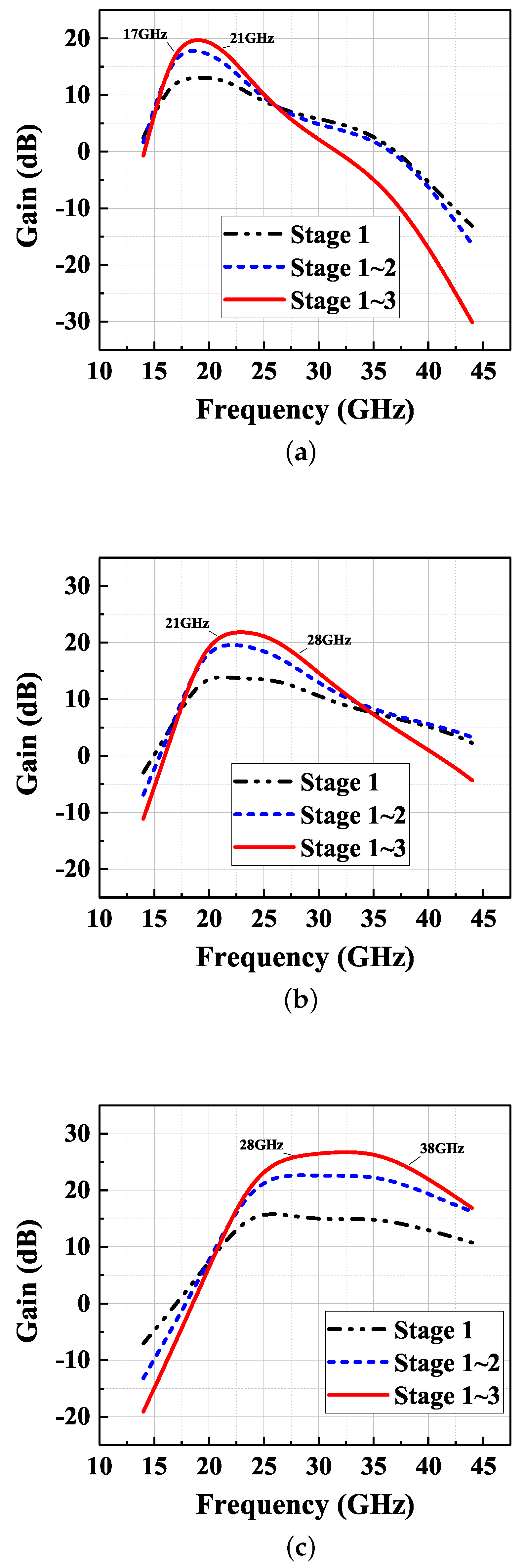
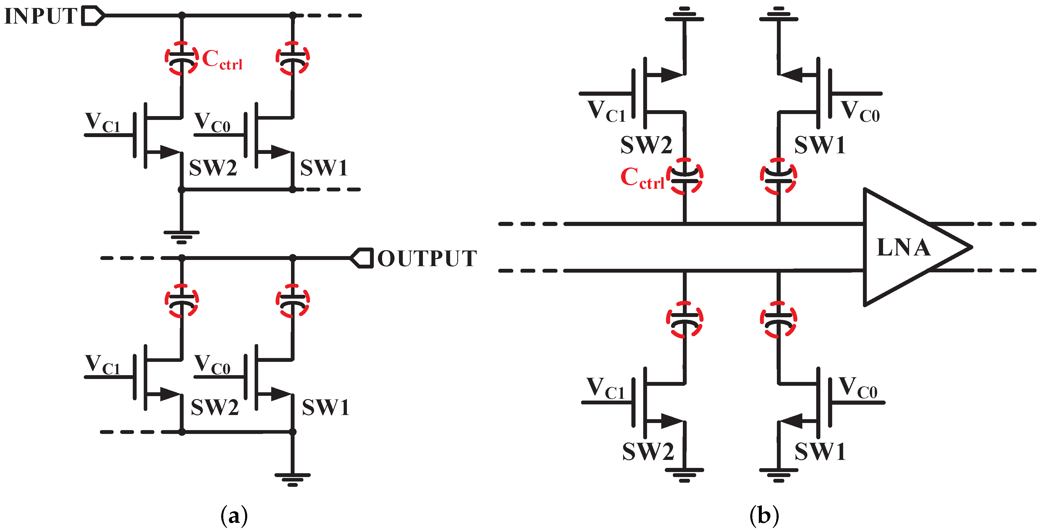
2.1. The Structure and Performance of the LNA
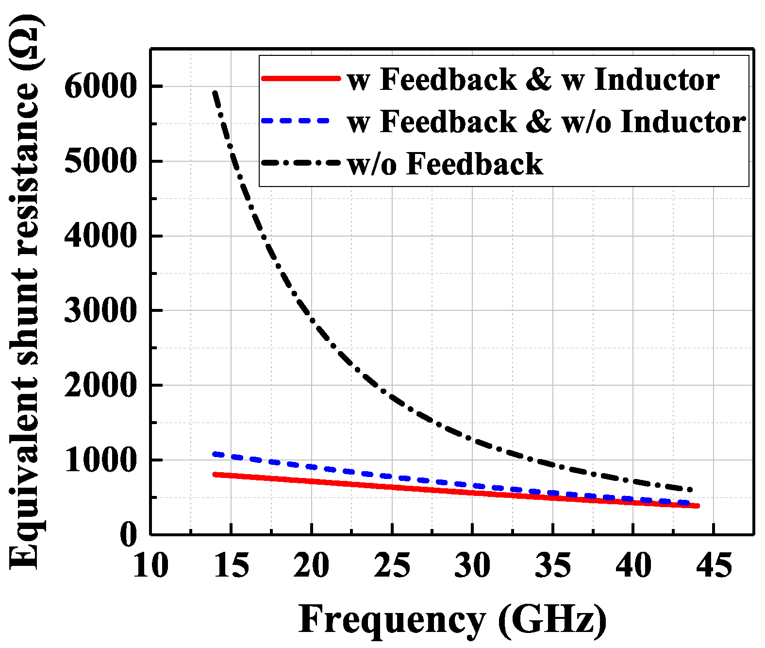
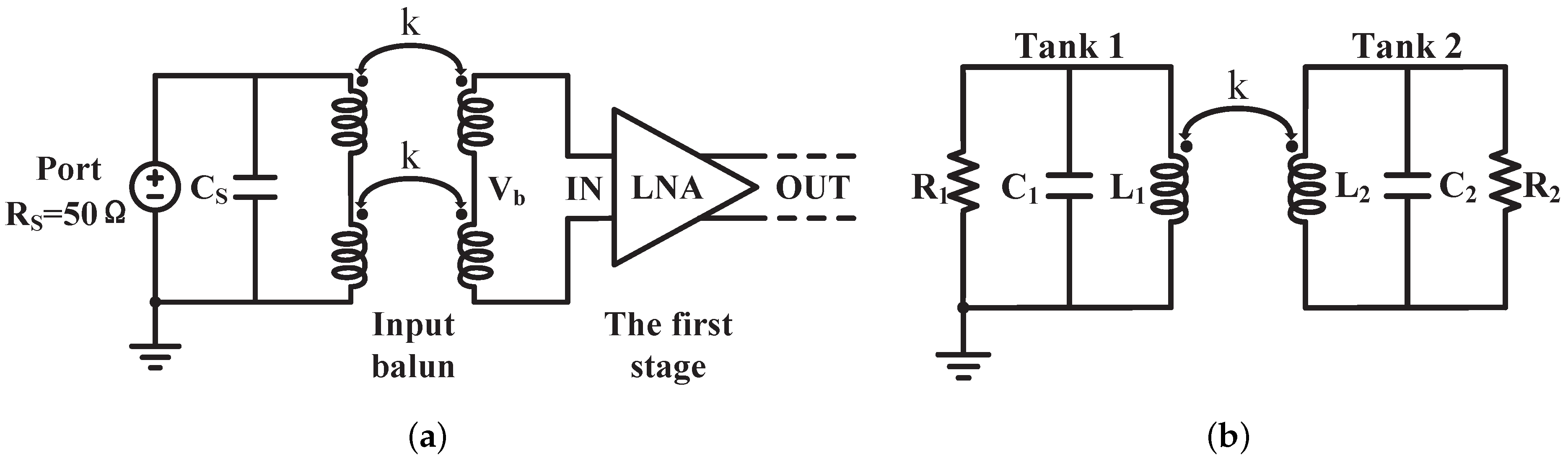
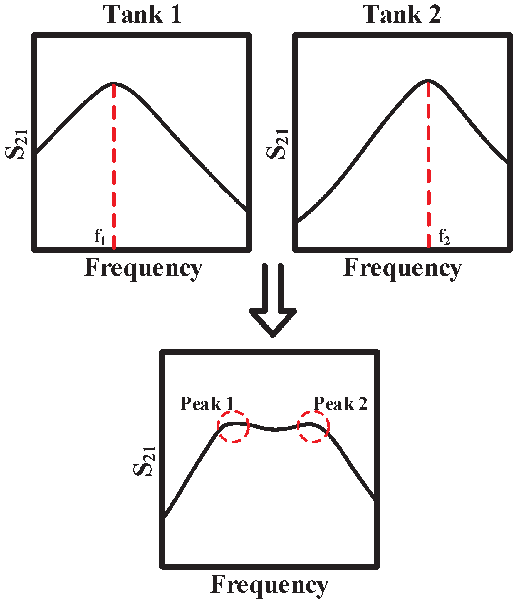
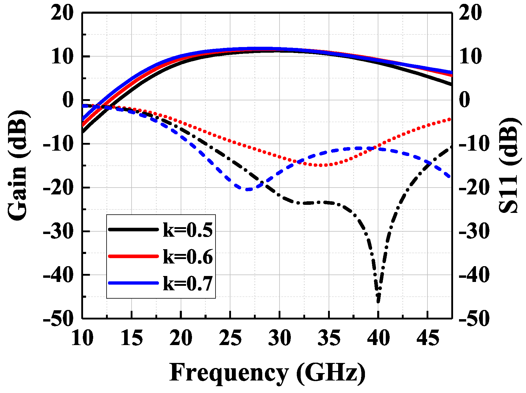
2.2. Magnetically Coupled Resonator(MCR) Matching Network
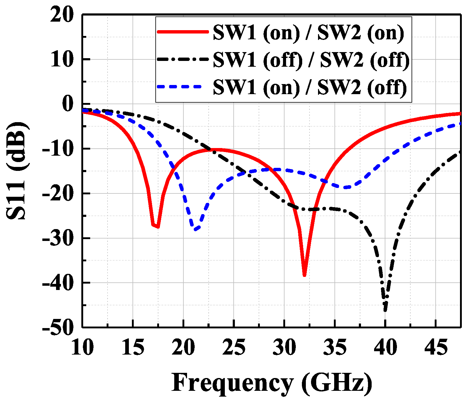
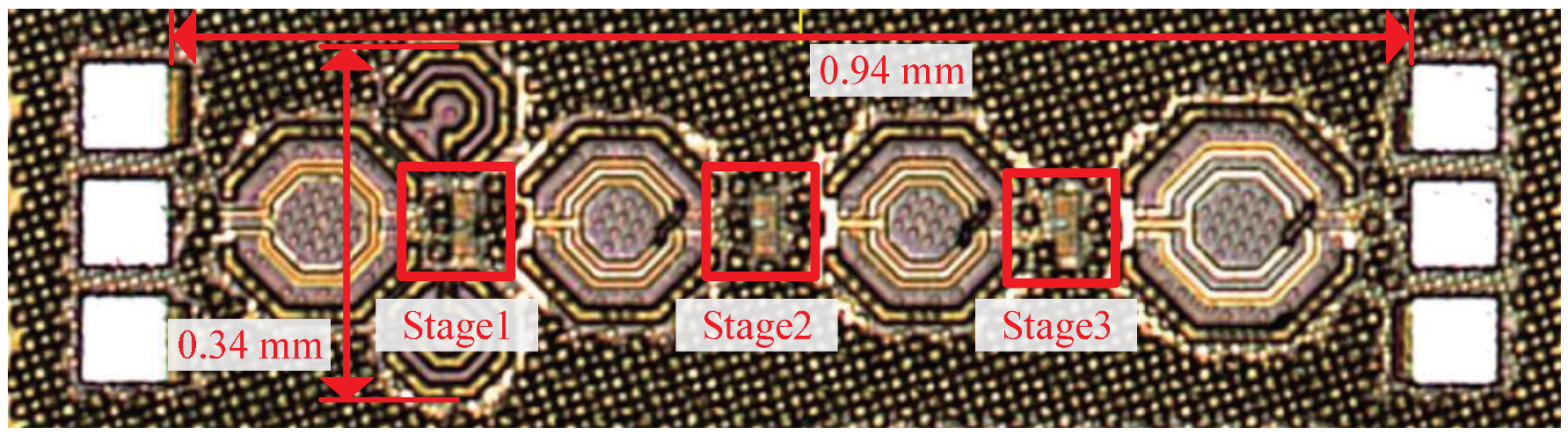
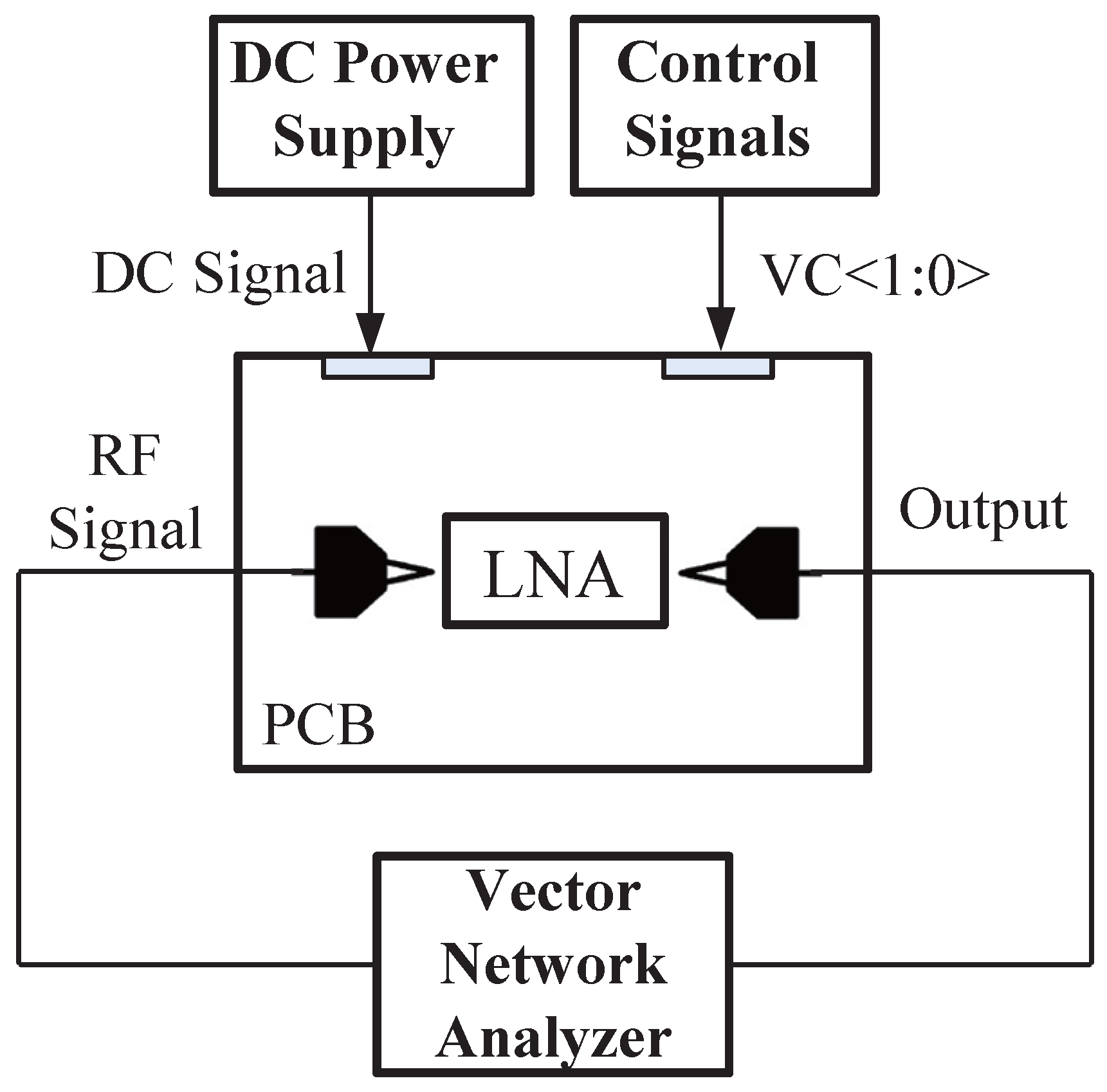
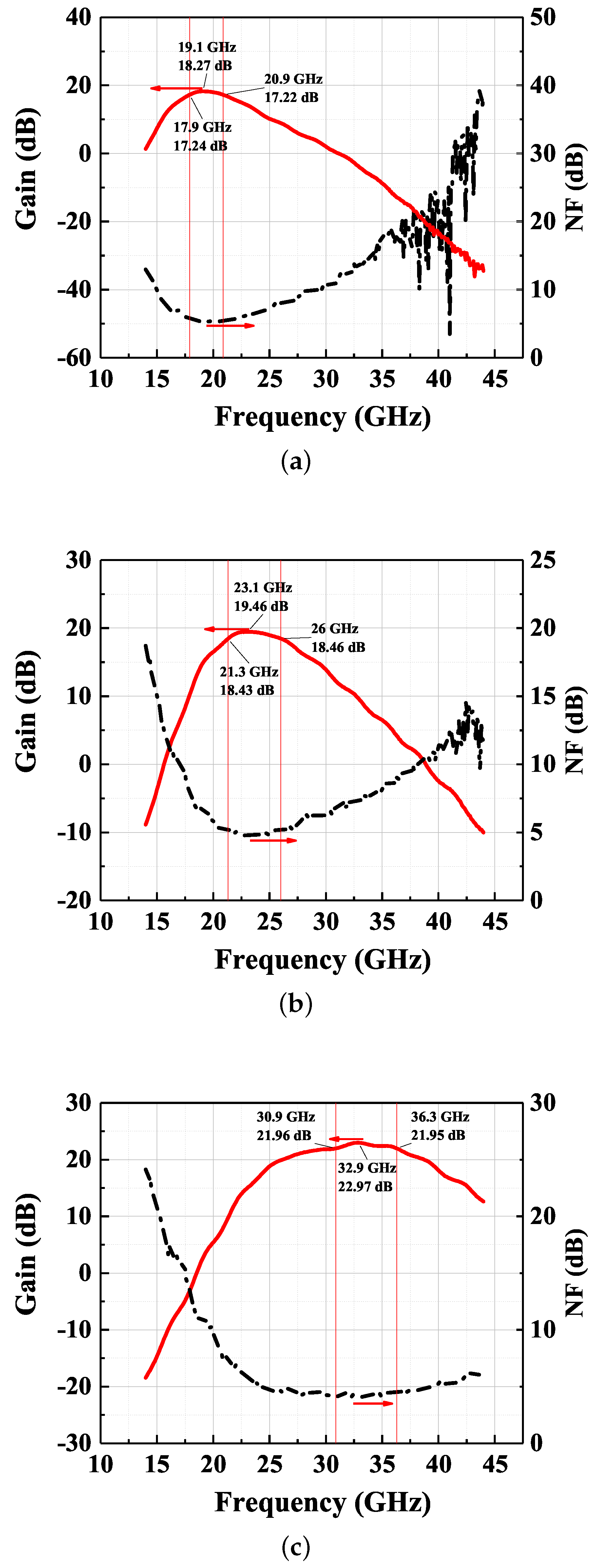
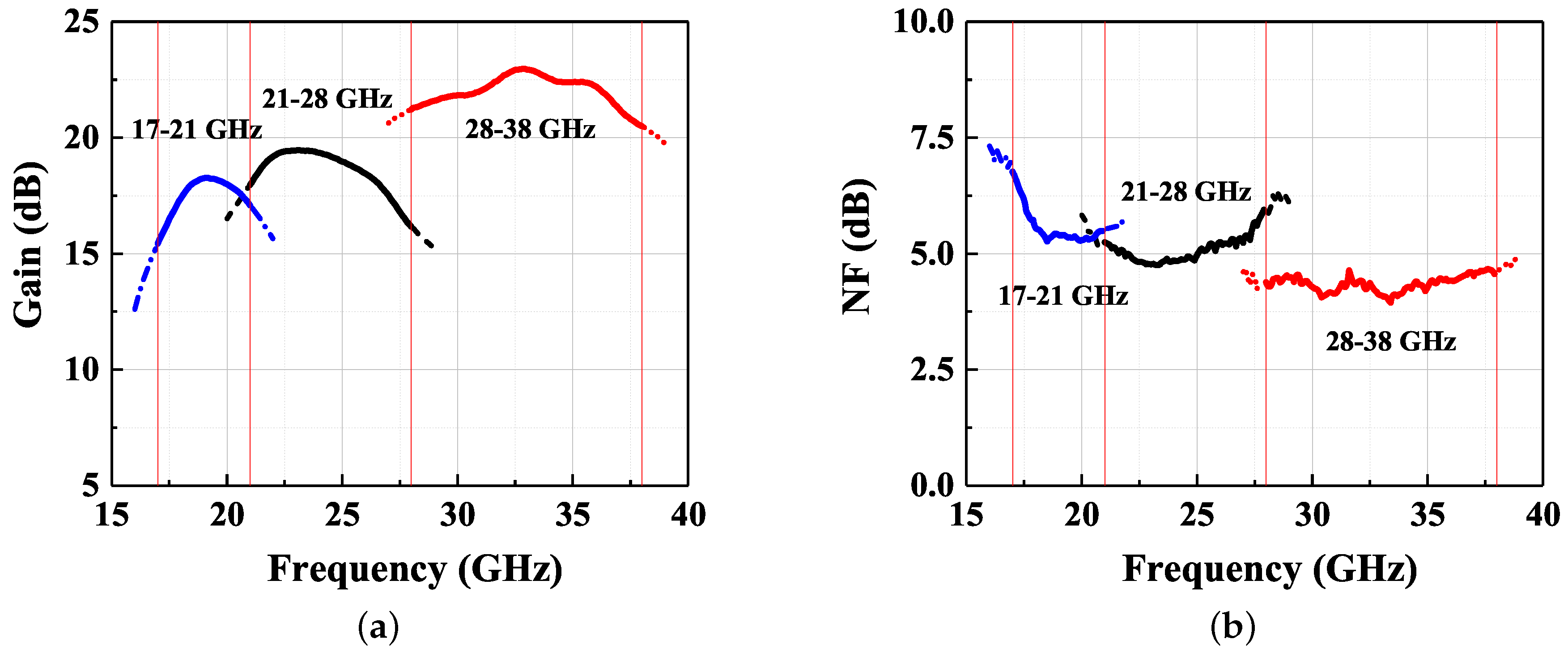
3. Measurement Results
4. Conclusions
Author Contributions
Funding
Conflicts of Interest
References
- Zhao, D.; Gu, P.; Zhong, J.; Peng, N.; Yang, M.; Yi, Y.; Zhang, J.; He, P.; Chai, Y.; Chen, Z.; et al. Millimeter-Wave Integrated Phased Arrays. IEEE Trans. Circuits Syst. I Regul. Pap. 2021, 68, 3977–3990. [Google Scholar] [CrossRef]
- Luo, P.; Liu, M.; Chen, L.; Gao, J.; Zhu, Z.; Yang, Y. A 2.99 dB NF 15.6 dB Gain 3–10 GHz Ultra-wideband low-noise amplifier for UWB systems in 65 nm CMOS. Analog. Integr. Circuits Signal Process. 2019, 101, 651–657. [Google Scholar] [CrossRef]
- Salvucci, A.; Longhi, P.E.; Colangeli, S.; Ciccognani, W.; Serino, A.; Limiti, E. A straightforward design technique for narrowband multi-stage low-noise amplifiers with I/O conjugate match. Int. J. Microw.-Comput.-Aided Eng. 2019, 29, e21833. [Google Scholar] [CrossRef]
- AuChang, K.C.; Lu, B.Z.; Wang, Y.; Chiong, C.C.; Wang, H. A 17.7–42.9-GHz Low Power Low Noise Amplifier with 83% Fractional Bandwidth for Radio Astronomical Receivers in 65-nm CMOS. In Proceedings of the Asia-Pacific Microwave Conference Proceedings, Hong Kong, China, 8 December 2020; pp. 507–509. [Google Scholar]
- Lei, H.-W.; Wang, Y.; Chiong, C.-C.; Wang, H. A 2.5–31-GHz High Gain LNA in 0.15-μm GaAs pHEMT for Radio Astronomical Application. In Proceedings of the Asia-Pacific Microwave Conference, Kyoto International Conference Center (ICC Kyoto), Kyoto, Japan, 6 November 2018. [Google Scholar]
- Zhang, H.; Fan, X.; Sinencio, E.S. A low-power, linearized, ultra-wideband LNA design technique. IEEE J. -Solid-State Circuits 2009, 44, 320–330. [Google Scholar] [CrossRef]
- Weng, R.M.; Liu, C.Y.; Lin, P.C. A Low-Power Full-Band Low-Noise Amplifier for Ultra-Wideband Receivers. IEEE Trans. Microw. Theory Tech. 2010, 58, 2077–2083. [Google Scholar] [CrossRef]
- Yousef, K.; Jia, H.; Pokharel, R.; Allam, A.; Ragab, M.; Kanaya, H.; Yoshida, K. Low-power, low-voltage CMOS ultra-wideband low noise amplifier for portable devices. In Proceedings of the 2013 Second International Japan-Egypt Conference on Electronics, Communications and Computers, Cairo, Egypt, 17 December 2013; pp. 68–70. [Google Scholar]
- Kundu, S.; Paramesh, J. A Transformer-neutralized 0.6 V VDD 17–29 GHz LNA and its application to an RF front-end. Analog. Integr. Circuits Signal Process. 2015, 83, 173–186. [Google Scholar] [CrossRef]
- Khavari, A.F.; Mafinezhad, K. A New UWB LNA with 15 dB Gain in 90 nm CMOS with Current Reuse Topology. In Proceedings of the 26th Iranian Conference on Electrical Engineering, Sadjad University of Technology, Mashhad, Iran, 8 May 2018; pp. 184–189. [Google Scholar]
- Lee, M.; Kwon, I. 3–10 GHz noise-cancelling CMOS LNA using gm-boosting technique. IET Circuits, Devices Syst. 2018, 12, 12–16. [Google Scholar] [CrossRef]
- Singh, V.; Arya, S.K.; Kumar, M. A 3–14 GHz, Self Body Biased Common Gate UWB LNA for Wireless Applications in 90 nm CMOS. J. Circuits Syst. Comput. 2019, 28, 1950056. [Google Scholar] [CrossRef]
- Chauhan, V.; Floyd, B. A 24–44 GHz UWB LNA for 5G cellular frequency bands. In Proceedings of the Global Symposium on Millimeter Waves, University of Colorado Boulder Campus, Boulder, CO, USA, 17 August 2018. [Google Scholar]
- Hadipour, K.; Ghilioni, A.; Mazzanti, A.; Bassi, M.; Svelto, F. A 40 GHz to 67 GHz bandwidth 23 dB gain 5.8 dB maximum NF mm-Wave LNA in 28 nm CMOS. In Proceedings of the Digest of Papers—IEEE Radio Frequency Integrated Circuits Symposium, Phoenix, AZ, USA, 17 May 2015. [Google Scholar]
- Xu, J.; Yan, N.; Zeng, X.; Gao, J.; Yang, C. A 3.4 dB NF K-band LNA with a tapped capacitor matching network in 65 nm CMOS technology. Int. J. Microw.-Comput.-Aided Eng. 2015, 25, 146–153. [Google Scholar] [CrossRef]
- Rostomyan, N.; Ozen, M.; Asbeck, P.M. Synthesis technique for low-loss mm-Wave T/R Combiners for TDD front-ends. IEEE Trans. Microw. Theory Tech. 2019, 67, 1030–1038. [Google Scholar] [CrossRef]
- Lee, S.; Park, J.; Hong, S. A Ka-Band Phase-Compensated Variable-Gain CMOS Low-Noise Amplifier. IEEE Microw. Wirel. Components Lett. 2019, 29, 131–133. [Google Scholar] [CrossRef]
- Razavi, B. A 60-GHz CMOS receiver front-end. IEEE J. -Solid-State Circuits 2006, 41, 17–22. [Google Scholar] [CrossRef]
- Harsoori, M.M.; Zulkifli, T.Z.A.; Abbas, U.; Sattar, S. A gain boosting single stage cascode LNA for millimeter-wave applications. In Proceedings of the Asia Pacific Conference on Postgraduate Research in Microelectronics and Electronics, Kuala Lumpur, Malaysia, 31 October 2017. [Google Scholar]
- An, X.; Wagner, J.; Ellinger, F. A 2.8 GHz to 12.8 GHz UWB LNA using transformer wide-band input matching for IR-UWB radar applications. In Proceedings of the Midwest Symposium on Circuits and Systems, Windsor, ON, Canada, 5 August 2018; pp. 93–96. [Google Scholar]
- Lokhandwala, M.; Gao, L.; Rebeiz, G.M. A high-power 24–40-GHz transmit-receive front end for phased arrays in 45-nm CMOS SOI. IEEE Trans. Microw. Theory Tech. 2020, 68, 4775–4786. [Google Scholar] [CrossRef]
- Yang, L.; Yang, L.A.; Rong, T.; Jin, Z.; Hao, Y. A five-octave broadband LNA MMIC using bandwidth enhancement and noise reduction technique. IEICE Electron. Express 2019, 16, 20190096. [Google Scholar] [CrossRef]
- Qin, P.; Xue, Q. Compact Wideband LNA with Gain and Input Matching Bandwidth Extensions by Transformer. IEEE Microw. Wirel. Components Lett. 2017, 27, 657–659. [Google Scholar] [CrossRef]
- Geha, C.; Nguyen, C.; Silva-Martinez, J. A wideband low-power-consumption 22–32.5-GHz 0.18-μm BiCMOS active balun-LNA with IM2 cancellation using a transformer-coupled cascode-cascade topology. IEEE Trans. Microw. Theory Tech. 2017, 65, 536–547. [Google Scholar] [CrossRef]
- Jia, H.; Prawoto, C.C.; Chi, B.; Wang, Z.; Yue, C.P. A full ka-band power amplifier with 32.9% PAE and 15.3-dBm Power in 65-nm CMOS. IEEE Trans. Circuits Syst. I Regul. Pap. 2018, 65, 2657–2668. [Google Scholar] [CrossRef]


| Frequency Band (GHz) | Maximum Gain (dB) | Minimum NF (dB) |
|---|---|---|
| 17–21 | 18.3 | 5.2 |
| 21–28 | 19.5 | 4.7 |
| 28–38 | 23.0 | 4.0 |
| Reference | Process | Architecture | Supply Voltage (V) | Bandwidth (GHz) | Gain (dB) | NF (dB) | FOM (GHz/mW) | Area (mm2) |
|---|---|---|---|---|---|---|---|---|
| [9] a | 0.13-μm CMOS | CG | 0.6 | 17.3-29.3 | 15.4 | 5.5–7 | - | 0.192 b |
| 1.2 | 17.3–29.3 | 18 | 4.7–6.2 | - | ||||
| [17] | 65-nm CMOS | Cascode | - | 30–34.5 | 20.8 | 3.71 | 1.4 | 0.39 |
| [16] | 45-nm CMOS SOI | Cascode | 1 | 24–30 | 11.2 | 3.2 | 0.7 | - |
| [23] | 65-nm CMOS | Cascode | - | 15.8–30.3 | 10.2 | 3.3–5.7 | 3.3 | 0.18 |
| [24] | 0.18-μm BiCMOS | Cascode | 1.8 | 22–32.5 | 18.6 | 4.5–5.5 | - | 0.46 b |
| This work | 45-nm CMOS SOI | Cascode | 1 | 17–21 | 18.3 | 5.2 | 4.9 | 0.42 b |
| 21–28 | 19.5 | 4.7 | ||||||
| 28–38 | 23.0 | 4.0 |
Publisher’s Note: MDPI stays neutral with regard to jurisdictional claims in published maps and institutional affiliations. |
© 2022 by the authors. Licensee MDPI, Basel, Switzerland. This article is an open access article distributed under the terms and conditions of the Creative Commons Attribution (CC BY) license (https://creativecommons.org/licenses/by/4.0/).
Share and Cite
Han, F.; Liu, X.; Wang, C.; Li, X.; Qi, Q.; Li, X.; Liu, Z. A Multi-Band LNA Covering 17–38 GHz in 45 nm CMOS SOI. Electronics 2022, 11, 3255. https://doi.org/10.3390/electronics11193255
Han F, Liu X, Wang C, Li X, Qi Q, Li X, Liu Z. A Multi-Band LNA Covering 17–38 GHz in 45 nm CMOS SOI. Electronics. 2022; 11(19):3255. https://doi.org/10.3390/electronics11193255
Chicago/Turabian StyleHan, Fang, Xuzhi Liu, Chao Wang, Xiao Li, Quanwen Qi, Xiaoran Li, and Zicheng Liu. 2022. "A Multi-Band LNA Covering 17–38 GHz in 45 nm CMOS SOI" Electronics 11, no. 19: 3255. https://doi.org/10.3390/electronics11193255