1. Introduction
With all-day, all-weather, and global observation capability, a spaceborne synthetic aperture radar (SAR) has been widely used in the fields of national defense and the military, geological and geomorphological mapping, and ocean observation. Due to the increased resolution of a spaceborne SAR, a phased array antenna is required to operate at a larger bandwidth, which has introduced the problems of beam dispersion and aperture crossing that need to be solved. The main method to solve these problems is to use a wideband true time delay line (TTDL) in combination with a phase shifter.
In recent years there has been much research on wideband TTDLs. Depending on the subject area, TTDLs can be classified into optical delay lines, acoustic delay lines, magnetic static wave (MSW) delay lines, and electrical delay lines. Optical delay lines [
1] are very small and have very low insertion loss, so they can be wound in large lengths in a small space to achieve a long delay time. However, these lines require complex optoelectronic conversion devices and are not suitable for planar microwave circuits and spaceborne SAR systems. In [
2,
3], microwave signals were converted to an MSW and a surface acoustic wave (SAW), respectively, to reduce the group velocity substantially and thus achieve high delay efficiency. Still, these methods require complex conversion devices and are not suitable for planar circuits and miniaturized devices. Considering the need for integration, miniaturization, and a large delay time in future spaceborne SAR systems, electric delay lines could be a good choice.
To date, electrical delay lines have mainly been implemented using planar transmission lines, such as microstrip lines [
4], strip lines [
5], and coplanar waveguides [
6]. Planar transmission lines have the advantages of low loss and cost, easy processing, and a compact structure, which make them well suited for high-frequency integrated components and systems. In [
7], a microstrip meander delay line structure was proposed to arrange microstrip lines in a curved shape on a single-layer PCB board to achieve a delay efficiency of 3.6 times in the X-band. Although this method is simple and efficient, the interline coupling problem can lead to large delay fluctuations of 16.6%. Therefore, if this method needs to be applied in practical engineering, it is necessary to increase the adjacent microstrip line spacing to reduce coupling, but this wastes much of the alignment area, which is not conducive to miniaturization.
In addition to the meander-shaped winding used to increase the delay efficiency, different microstrip structures have been designed to achieve the slow wave effect. In [
8], a left-handed transmission line (LHTL) method was proposed to modify the conventional transmission line to enhance the slow wave effect by using microstrip cross-fingers and ground inductance. Based on the results presented in [
8], in [
9], the size of the left-handed transmission line was reduced to 58% of the original size, and the delay time was increased, while the structure was more compact. The delay of 1.3 ns was achieved in the range of 2 GHz–4 GHz at a 30 mm length. However, the delay efficiency was not high, and the total delay time was short.
There have also been a number of studies based on the substrate integrated waveguide (SIW) [
10]. In [
11,
12], the authors loaded microstrip polylines and inductive capacitors on the SIW to achieve the slow wave effect, respectively. This reduced the phase velocity by 35%, but the intra-band delay fluctuations were too large, and the introduction of complex microstrip polyline patterns and inductive capacitors increased the processing and fabrication difficulties.
In recent studies, micro-coaxial technology [
13] has been used to implement delay lines. Micro-coaxial transmission lines have low loss and no dispersion. Thus, even when multiple micro-coaxial transmission lines are transmitted side by side, no interline coupling phenomenon is generated, and micro-coaxial transmission lines can be wired in three dimensions, which saves space and improves delay efficiency significantly. However, micro-coaxial transmission lines have the problems of high processing, manufacturing difficulties, and high costs. Based on a micro-coaxial transmission line, a substrate integrated coaxial line (SICL) structure was proposed in [
14]. In SICL, a section of a transmission line is added to the structure similar to the SIW to simulate the coaxial line structure. In this way, the advantages of the planar transmission line and micro-coaxial structure of good shielding, low loss, low cost, easy processing, and easy-to-realize three-dimensional (3D) wiring are combined.
In summary, the current problems of the delay line-related research mainly include low delay efficiency, short delay time, narrow working bandwidth, and low structural integration. Future research on feasible engineering applications should consider a wideband structure with good shielding that can be wired in three dimensions.
Motivated by the previous studies, this paper proposes a new 3D ultra-wideband efficient large delay structure based on the SICL and MDL, named the substrate integrated coaxial meander line (SICML). In the proposed structure, the center transmission line of a substrate integrated coaxial line is replaced with a suitable meander line structure. Additionally, the delay multiplier is up to eight-fold better than other studies of the same type, and the delay line width is only 2 mm. In addition, this paper designs a reasonable turn structure and vertical transition structure, whose good shielding performance allows the realization of the planar tight-adjacent and 3D wiring, thus significantly saving space. Moreover, the 3.1 ns and 6.4 ns delay lines are designed and experimentally tested, and the results indicate that the working band of the proposed structure is 4 GHz–10 GHz. The outstanding advantages of the proposed SICML structure are: its 85.7% ultra-broadband performance, large delay times of 3.1 ns and 6.4 ns, and delay multiplier being up to eight times better. The measurement results are in good agreement with the simulation results, which proves certain engineering practical application value of the proposed delay line structure.
This paper is organized as follows:
Section 2.1 presents the proposed SICML structure’s design process, parameter settings, and simulation results. Three types of transition structures are presented in
Section 2.2, where their different transition functions and design approaches are also described.
Section 3 gives the measurement results of the proposed SICML structure. Finally,
Section 4 summarizes the key research contributions and presents the future research directions.
2. Design and Simulation
A meander delay line (MDL) has advantages of a simple design, easy miniaturization, easy processing, low cost, and high delay efficiency, but its main disadvantages are that the adjacent meander transmission line generates interline coupling in the in-plane and 3D wiring, and the space must be sacrificed to ensure good frequency characteristics. In contrast, the SICL has advantages of good shielding, easy 3D integration, and easy processing. Therefore, the SICL and MDL can be combined to form a SICML, which can realize both flat adjacent and 3D wiring while significantly saving space and greatly improving delay efficiency, which has high research and practical engineering value.
2.1. Substrate Integrated Coaxial Meander Line
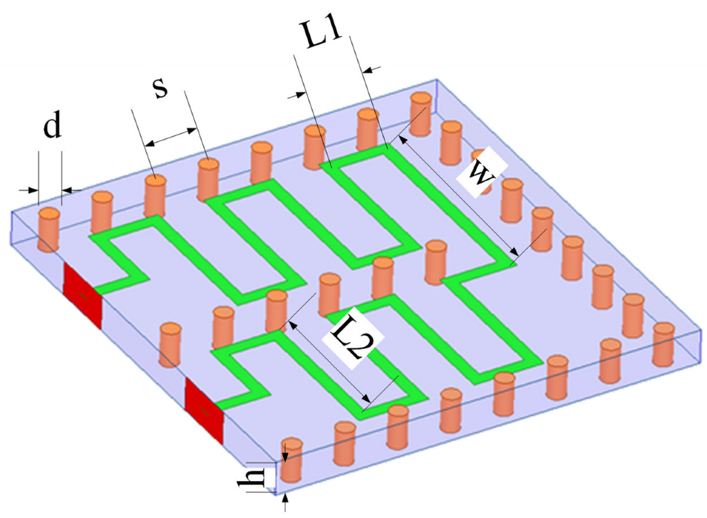
As shown in
Figure 1, in the SICL center area there is a section of transmission line, and at the top and bottom of the SICL, there are two ground surfaces and two rows of metal vias on the side forming the analog coaxial structure. This structure is similar to the structures of the SIW and strip line. Therefore, the SICL belongs to the class of TEM mode transmission lines.
Since the transmission line in the substrate center does not affect the electromagnetic field propagation pattern, the propagation characteristics of the SICL can be analyzed according to the propagation characteristics of the SIW. To control the radiation loss caused by the discontinuous metal through-hole sidewalls, in [
15], the authors summarized the conditions under which the transmission characteristics of the SIW are equivalent to those of a rectangular waveguide as follows:
where
weff denotes the equivalent rectangular waveguide width;
c is the free-space speed of light,
w is the spacing between the two rows of metal vias;
d is the diameter of the metal vias;
s is the spacing between adjacent metal vias;
fTE10 is the designed TE
10-mode cutoff frequency;
er is the relative dielectric constant of the substrate; and in this study, Rogers RO3006 substrate with a relative permittivity of 6.15 is used.
Considering the requirements of the actual engineering processing, the adjacent metal through-hole spacing s and metal through-hole diameter d are set to 0.5 mm and 0.25 mm, respectively. The substrate height h does not have an impact on the propagation mode, so a commonly-used substrate thickness of 0.254 mm is adopted. According to Equations (1)–(4), w is the only parameter that determines the substrate integrated coaxial line TE10-mode cutoff frequency fTE10.
When selecting the
w value, two aspects have to be considered. First, the group delay near the cutoff frequency
fTE10 will produce large fluctuations, so it is necessary to set
fTE10 as far as possible from the high cutoff frequency of 10 GHz in the frequency band of interest. Second, the proposed delay line needs to be wired in both two and three dimensions, so
w should be as small as possible to save space, and it should leave space for the introduction of a meander delay line (MDL) in the next step. Considering the two mentioned aspects, the
w value is set to 2.1 mm, and
fTE10 is set to 30 GHz according to Equation (5), which fully satisfies the two above requirements. Equation (5) is a variation of Equation (4).
In addition, to avoid the reflection problem caused by an impedance mismatch, the characteristic impedance of the SICL needs to be 50 Ω. However, the characteristic impedance of the SICL depends on the central transmission line width
W2 value. Since the center transmission line propagation environment of the SICL is similar to that of a strip line, the characteristic impedance can be approximated to [
16]:
The center transmission line width W2 obtained by Equation (6) is optimized by simulation using the commercial finite element method (FEM) software Ansoft HFSS, and the final center transmission line width is obtained to be W2 = 0.16 mm.
The HFSS simulation results of the SICL designed according to the above-mentioned parameters are shown in
Figure 2. A 30 mm length of the SICL in the frequency band of 4 GHz–10 GHz has the S21 (IL) of more than −0.17 dB, S11 (RL) of less than −34 dB, and a group delay (GD) between 249.85 ps and 249.63 ps, which fully meets the design index requirements.
The SICL is a type of coaxial structure where the metal that passes through holes on both sides simulate the conductor sidewalls of the coaxial line. However, the SICL also has a strip line structure because the strip line can be regarded as a derivative of the coaxial line. When the coaxial line is turned into a rectangular structure, the vertical conductor sidewalls on both sides become a strip line when they are infinite. Therefore, the SICL can be analyzed according to the strip line theory, and the idea of increasing the delay efficiency of the strip line can be applied to the SICL. Following this idea, this paper applies the meander strip delay line to the SICL so that their advantages can be fully used and the 3D ultra-broadband large delay effect can be realized.
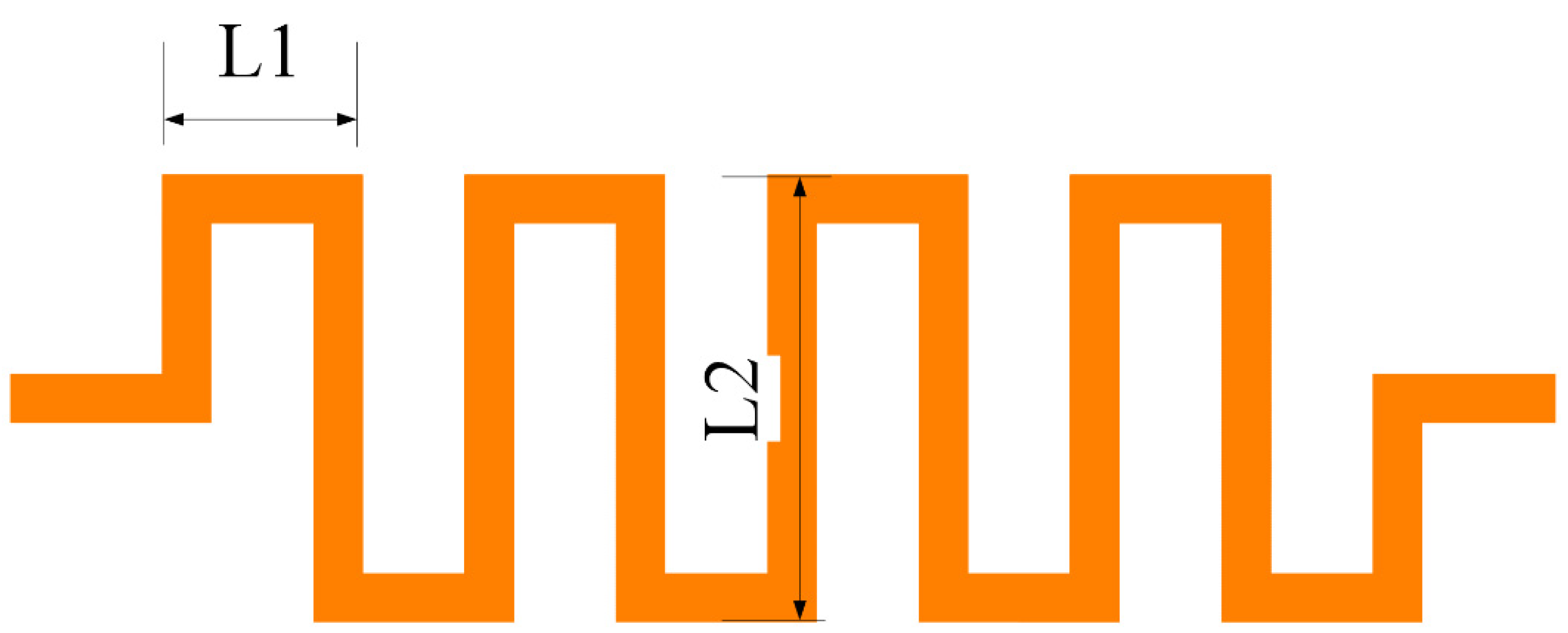
The meander line structure is shown in
Figure 3. The parameters affecting the delay efficiency and RL of the meander line mainly include the cell’s length
L1 and width
L2. The values of
L1 and
L2 are optimized separately using the HFSS, and the optimization objective was to reduce the RL while maximally increasing the delay time. The optimized values were obtained as
L2 = 2 ×
L1 = 1 mm. In addition, the center transmission line of the SICL is replaced by the above-designed meander line structure to obtain the proposed SICML structure, as shown in
Figure 4.
The HFSS simulation results are shown in
Figure 5, where it can be seen that in the frequency band of 4 GHz–10 GHz, the 30 mm SICML has IL of more than −0.59 dB, RL less than −20.63 dB, and GD between 762.60 ps and 813.67 ps. According to the simulation results, compared with the SICL structure, not only is the delay efficiency improved by 224%, but also the IL and RL are within the reasonable range.
2.2. Three Types of Transition Structures
Since the SICML has good shielding, it can easily realize nearly planar wiring without considering the coupling problem of adjacent curved lines, while the 3D wiring can be realized to reduce the delay line volume significantly and realize miniaturization. Therefore, an appropriate design of a planar turn structure and a vertical transition structure is crucial to ensure that the frequency characteristics of the delay line after the turn and vertical connection are optimized.
In addition, because the SICML is a coaxial structure, the transmission line is located in the center of a two-layer dielectric substrate. Therefore, it is not easy to perform the experimental test using this structure, so it is necessary to optimize a transition structure of the SICML and microstrip line to facilitate the installation of SMA for testing.
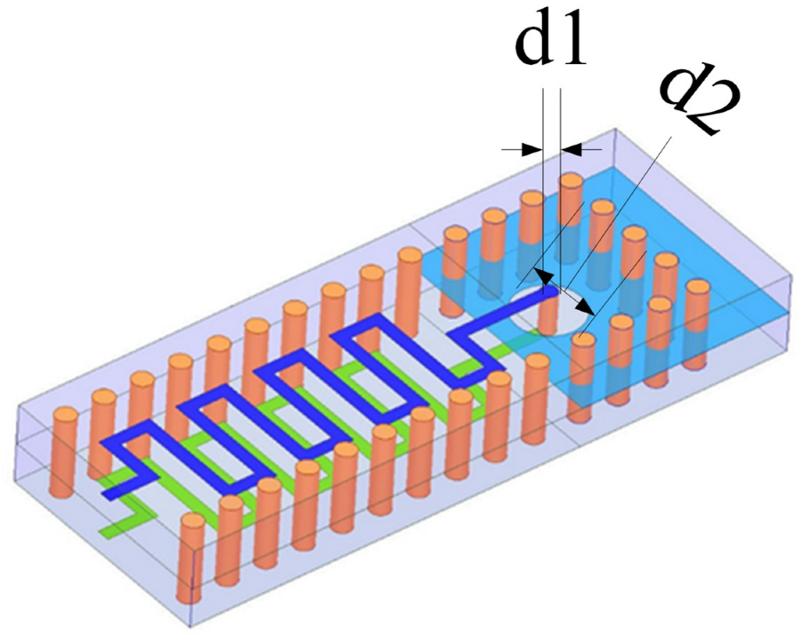
The design principle of a planar turning structure is very simple since the structure of the central transmission line of the turning part is similar to the SICML, the metal through-hole sidewalls need to be set on both sides of the central transmission line of the turning structure, which can save space. The planar turning structure designed by simulation optimization is shown in
Figure 6.
The optimized planar turn structure is applied to the proposed SICML for planar tight-adjacent wiring, as shown in
Figure 7. The HFSS simulation results of the obtained structure are shown in
Figure 8, where it can be seen that in the frequency band of 4 GHz–10 GHz, the 30 mm delay line had IL of more than −1.32 dB, RL less than −19 dB, and GD between 1.53 ns and 1.64 ns. Thus, the designed planar turn structure had little effect on the SICML performance and could perfectly meet the miniaturization requirement of planar tight-adjacent wiring.
In designing the vertical transition structure suitable for the SICML, this study follows the previous research [
17,
18], and the proposed design is presented in
Figure 9. The proposed structure is connected vertically using a 0.2 mm metal blind hole, and the GND in the middle of the two signal layers is sheared using an appropriately-sized circular surface to ensure the electromagnetic wave transmission between the upper and lower signal layers. The simulation results of the proposed vertical transition structure are shown in
Figure 10, where it can be seen that the vertical structure for 3D wiring with a 30 mm delay line and a total height of 1 mm had IL of more than −1.34 dB, RL less than −21.32 dB, and GD between 1.56 ns and 1.67 ns. Thus, the designed vertical transition structure fully met the 3D wiring requirements.
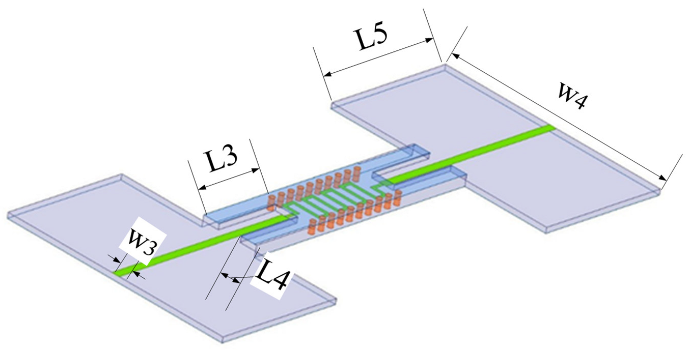
The microstrip transition structure designed in this paper is shown in
Figure 11. As shown in
Figure 11, between the SICML and the microstrip line, the middle part of the substrate on the SICL is hollowed out to expose the central transmission line part, which helps to mitigate sudden electric field changes at the transition point. The width of the microstrip line portion is designed to be larger to match the SMA connector size and facilitate subsequent installation testing. This transition structure is loaded onto both sides of the 30 mm SICML presented in
Section 2.1. The obtained structure was simulated, and the obtained simulation results are shown in
Figure 12. The simulation results showed that this structure had IL of more than −0.78 dB, RL less than −25 dB, and GD between 900 ps and 958 ps in the frequency band of 4 GHz–10 GHz. Thus, the RL was optimized, and the group delay jitter was reduced compared to the case without the microstrip transition structure. Therefore, the designed microstrip transition structure can be used in the proposed SICML structure.
Considering that most current studies on wideband true time delay lines have reported short delay times, the delay line structures presented in
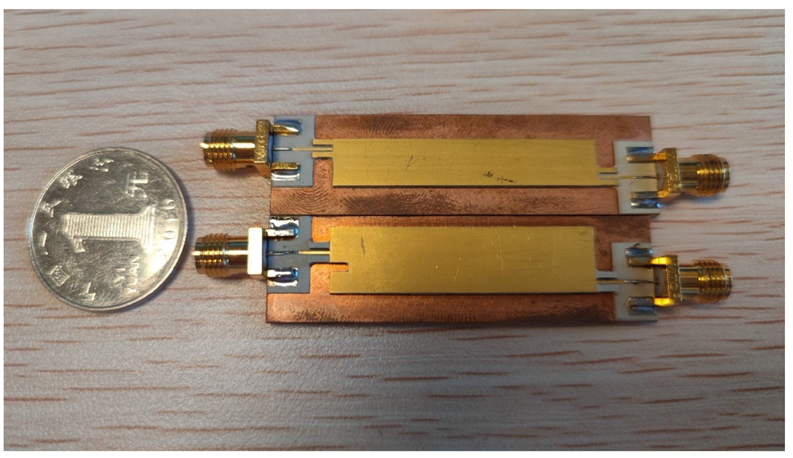
Figure 13 were designed with a delay time of 3.1 ns and 6.4 ns and tested to prove that the proposed delay line structure can achieve a longer delay time through planar and three-dimensional wiring. The dimensions of the 3.1 ns and 6.4 ns structures were 38 mm × 7 mm × 0.5 mm and 37 mm × 9.2 mm × 1 mm, and they included three and five PCB layers, respectively.
The simulation results of the two delay lines with a large delay time are shown in
Figure 14. The 3.1 ns delay line had IL of more than −2.67 dB, RL less than −22 dB, and GD between 3.0 ns and 3.2 ns. Meanwhile, the 6.4 ns delay line had IL of more than −5.54 dB, RL less than −24 dB, and GD between 6.23 ns and 6.6 ns. The simulation results meet the design expectations, and the RL index leaves a margin for subsequent experimental tests.
3. Experimental Results and Discussion
The diagram of the proposed SICML structure with dimensions of 38 mm × 7 mm × 0.5 mm and 37 mm × 9.2 mm × 1 mm is presented in
Figure 15. The S-parameters and group delay of the proposed structure were tested using a vector network analyzer, and the measurement results are shown in
Figure 16.
The measurement results show that the ILs of the 3.1 ns and 6.4 ns delay lines were larger than −5.38 dB and −10.69 dB, respectively. The RL of the two lines was basically less than −15 dB. The measured delay time was close to the simulated one, but the delay fluctuations were increased to 6% and the loss represented by the S-parameter increased. The reason for a slight difference between the simulated and measurement results could be the error caused by the processing and manufacturing of the substrate. The proposed delay line is designed on RO3006 substrate, but because the design of this delay line requires high accuracy of the process, there will be a large error in manufacturing on the RO3006 substrate. After using X-ray to irradiate the delay line, it was found that the position of many isolation vias deviated significantly from the design drawing. This will undoubtedly lead to the deterioration of the actual measurement results. Considering the degree of refinement of the proposed structure in this paper, subsequent design and measurement can be performed on low-temperature co-fired ceramic (LTCC) substrates.
However, one more point is worth noting. The GD of the proposed SICML structure increases linearly with frequency. The reason for the GD dispersion phenomenon is that the line spacing
L1 of MDL is too small, thus creating coupling. In
Section 2.1, HFSS’s optimization objective was to reduce the RL while maximally increasing the delay time, and did not take into account the GD dispersion phenomenon. Considering this further, this may also be one of the reasons for the increased delay fluctuations.
A wideband phase shifter can be used to perform GD dispersion equalization. The phase shifters have a phase offset φ = 2πftGD that does not change with frequency, so the group delay tGD decreases as the frequency f increases. For the 3.1 ns delay line, the GD dispersion range is 2.9 ns−3.18 ns, which requires a phase shifter with a phase shift range of at least 705.6°. Therefore, a 720° wideband phase shifter can be used to equalize the GD dispersion phenomenon of the SICML structure.
However, this problem can also be solved by increasing the line spacing
L1. The comparison of the simulation results before and after the increase in line spacing
L1 is shown in
Figure 17. The GD dispersion phenomenon is significantly improved by increasing
L1. Although there is still a slight GD dispersion, this degree of dispersion can be compensated for by using a 93° phase shifter.
A comparison of the research results presented in this paper with the existing research results is shown in
Table 1.
Table 1 shows that most of the current delay lines based on substrate integration technology have a small delay time, even less than 1 ns, and the delay time of the SICML structure proposed in this paper reaches 6.4 ns, which is much higher than other studies of the same type. Although in
Table 1 the insertion loss of the delay line proposed in this paper is larger than that of other studies, if both the delay time and insertion loss are considered, the delay line proposed in this paper has a smaller insertion loss for the same delay time. In the case of the large delay time, the insertion loss of the delay line will inevitably increase, which will significantly affect the phased array performance. Therefore, delay lines need to be used in conjunction with bi-directional amplifiers. To ensure a fair comparison, a delay line structure of this paper with the same delay time as the delay line proposed in [
7] is simulated. It can be seen that the proposed delay line has less volume, larger delay multiplier, and less delay fluctuation for the same delay time case.
As shown in
Table 1, compared with the related research, the proposed SICML has significant advantages in delay time, delay multiplier, and relative bandwidth; namely, the delay time, delay multiplier, and relative bandwidth are improved by 2.13–160 times, 1.025–6.8 times, and 2.14–3.86 times, respectively.
The delay fluctuations shown in
Table 1 range from 5% to 16.6%. Although the proposed SICML structure’s delay fluctuations, which are due to manufacturing errors and unreasonable MDL line spacing settings, reach 6%; even so, the delay fluctuations in this paper still have some advantages compared to other studies. In addition, many delay line papers do not give delay fluctuation parameters, which may be due to large delay fluctuations. The introduction of the delay structure leads to an increase in delay fluctuations, and it appears that delay fluctuations, delay efficiency, and delay line volume are a trade-off. As with the method mentioned above, increasing the line spacing
L1 reduces the delay fluctuation, but also increases the delay line volume.
In summary, the proposed structure represents an ultra-wideband high-efficiency large delay line whose IL and RL are within a reasonable range. However, it should be pointed out that the delay fluctuations of the proposed delay line need to be reduced to meet the requirements of the phased array antenna system for spaceborne SAR. Therefore, there is still much room for further improvement, and in-depth research should be continued in the future.


