Article

Generalized Carrier Index Differential Chaos Shift Keying Based SWIPT with Conversion Noise and Path Loss-Effect

College of Physics and Electronic Science, Guizhou Normal University, Guiyang 550001, China
*
Author to whom correspondence should be addressed.
Electronics 2022, 11(15), 2406; https://doi.org/10.3390/electronics11152406
Submission received: 8 July 2022 / Revised: 24 July 2022 / Accepted: 28 July 2022 / Published: 1 August 2022
(This article belongs to the Special Issue Multirate and Multicarrier Communication)

Abstract

:
A generalized carrier index differential chaos shift keying with simultaneous wireless information and power transfer (GCI-DCSK SWIPT) scheme, is proposed, which is an improved scheme for CI-DCSK SWIPT. Compared to CI-DCSK SWIPT, GCI-DCSK SWIPT is not only more flexible in selecting both index bit number and index carrier number, but also is more practical for considering both path loss and the conversion noise generated by radio frequency (RF) band to baseband. The proposed scheme applied a time-switching manner to harvest the energy carried by the inactive carriers. Theoretical bit error rate (BER) expressions of the scheme over AWGN and multipath Rayleigh fading channels are derived, and the ratio of harvested energy to transmitted energy is derived to desecribe the probability of self-sufficiency on power supply. In addition, the frame-derived factor and the energy carried by inactive carriers are optimized to obtain better BER performance. Simulation results show that taking both path loss and conversion noise into consideration, the scheme is still self-sufficient with good BER performance. Furthermore, by adjusting the number of active carriers of GCI-DCSK SWIPT, some cases of GCI-DCSK SWIPT outperform conversion noise-aware CI-DCSK SWIPT in BER.

1. Introduction

With the rapid development of 5G and Internet of things (IoT), the sensor nodes in wireless sensor networks (WSNs) are growing exponentially, which results in the relative shortage of spectrum resource and energy in wireless communication networks.
DCSK is the most popular chaos-based incoherent digital modulation scheme, which is outstanding for low-power and anti-fading [1,2]. It is considered as an excellent solution for energy limited WSNs. In the conventional DCSK scheme [3], the reference chaotic signal is transmitted during the first half of bit duration, and the information-bearing signal is transmitted during the second half of bit duration, which results in low energy efficiency (EE) and data rate. Hence, to improve various performances of DCSK, a large number of variants have been derived. A new short reference orthogonal double bit rate differential chaotic shift keying (SR-ODBR-DCSK) communication scheme is proposed in [4], which utilizes the orthogonality of chaotic signals to transmit odd information bits and even information bits and doubles transmission rate. A new fractional-order multi-carrier M-ary differential chaos shift keying system with multilevel code-shifted modulation (MC-MDCSK-MCS) is introduced in [5], which employs multiple subcarriers to transmit multiple MCS-MDCSK-modulated signals simultaneously and achieves higher bit rate. Index modulation (IM) [6] uses indexes of carriers to transmit information bits, which effectively adjusts spectrum efficiency (SE) and EE of the system. In the past few years, systems combined DCSK with code index [7,8], multi-carrier index [9,10,11,12], and position pulse modulation (PPM) index [13] have been proposed, which reduce the power consumption while effectively improving the BER performance compared to DCSK.
Simultaneous wireless information and power transfer (SWIPT) [14] is an excellent solution for energy-limited WSNs, which transmit information and energy simultaneously by wireless signal without requiring additional signals or spectrum. As incoherent-enabled SWIPT schemes have the advantages of low energy consumption and low complexity without requiring channel estimation, they have become an excellent alternative to coherent-enabled SWIPT. Over the past decade, plenty of research has been extensively devoted to designing SWIPT schemes based on DCSK. Ref. [15] investigates a buffer-aided DCSK-SWIPT relay system, which employs a decode-and-forward protocol without acquiring channel state information. Ref. [16] presents a DCSK-based wireless power transfer architecture, which employs an analog correlator at the receiver to boost the energy harvesting (EH) performance. Ref. [17] introduces two carrier index differential chaos shift keying with simultaneous wireless information and power transfer (CI-DCSK SWIPT) schemes that employ time switching, which reduce the transmission energy consumption and have excellent BER performance. However, in CI-DCSK SWIPT systems, the number of index carriers is limited to power-of-2 and the number of active carriers can only be 1 or n 1 ; thus the performance and the flexibility of the system are limited. To overcome the disadvantages of CI-DCSK SWIPT, GCI-DCSK which can flexibly adjust the number of index carriers and active carriers is combined with SWIPT. As both path loss and the noise generated by RF signal to base-band conversion are not considered in CI-DCSK SWIPT, which are very important for SWIPT-based systems to be consistent with the actual situation. Hence, a GCI-DCSK SWIPT scheme integrating GCI-DCSK with SWIPT is investigated in this paper, which not only improves the flexibility, but also takes the path loss and the conversion noise into consideration. The BER performance, sustainability, EE, and SE of the proposed system are analyzed. Moreover, the performance of GCI-DCSK SWIPT is compared with those of CI-DCSK1/2 SWIPT and GCI-DCSK, respectively.
The rest of this paper is organized as follows. In Section 2, the system is introduced. In Section 3, we introduce the BER, sustainability, EE, and SE of the system. In Section 4, the simulation and results analysis are carried out. In Section 5, the conclusion is given.

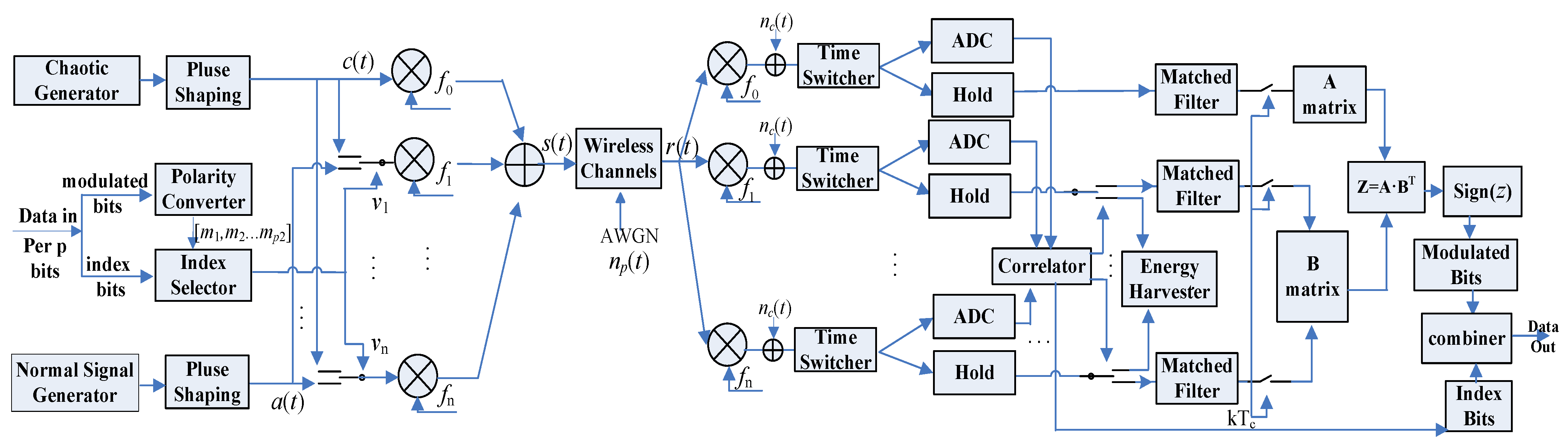
2. System Model of GCI-DCSK SWIPT

CI-DCSK SWIPT schemes [17] employ a one-to-one mapping between subcarrier activation patterns and index symbols, where the number of subcarriers n is chosen as 2 p 1 ( p 1 being the number of index bits) and the number of active carriers p 2 can only be 1 or n 1 . Hence, both the performance and the flexibility of the system are limited. To overcome the disadvantages of CI-DCSK SWIPT, GCI-DCSK SWIPT which can flexibly adjust the number of index carriers and active carriers is studied. Moreover, the path loss and the conversion noise are also taken into consideration.

2.1. Transmitter

As shown in Figure 1, there are total n + 1 carriers with indexes from 0 to n, where n could be any integer greater than 2. The reference chaotic signal is transmitted through the 0th carrier; the other n carriers transmit noise-like signals or modulated bits. The carrier statuses are determined by the index bits through the combination method [6].
A normally distributed signal with zero mean and variance of N s is sent if the carrier is inactive. Otherwise, the modulated bits are sent on the active carriers. During each frame, p bits will be transmitted, containing p 1 index bits and p 2 modulated bits. p 1 is usually set to log 2 C n p 2 , where C n p 2 denotes the number of p 2 combinations from n elements, · denotes the floor function, and p 2 is an integer between 1 and n 1 . First, modulated bits are changed into polarity bits through a polarity converter and the xth ( 0 x p 2 ) polarity bit is labeled as m x , where m x 1 , + 1 . Based on index bits and polarity bits, the index selector will generate a control sequence V for the n branches by employing the combinatorial method. v i corresponding to the xth active carrier is m x , and v i corresponds to each inactive carrier is 0. Then, the branch will be connected to the chaotic generator while v i being 1 or 1; otherwise, it will be connected to the normal signal generator. Therefore, the transmitted signal is expressed as
s ( t ) = cos ( 2 π f 0 t + ϕ 0 ) + i = 1 n v i cos ( 2 π f i t + ϕ i ) P s c ( t ) + i = 1 n v ¯ i cos ( 2 π f i t + ϕ i ) μ P s a ( t ) ,
where f i is the frequency of the ith subcarrier, ϕ i represents the phase angle on the carrier modulation, and P s denotes the transmitted power of the active carrier. The chaotic signal is c ( t ) = k = 1 β c k h t k T c , where h ( t ) is the square-root-raised-cosine filter, β is the spread spectrum factor, and T c is the chip interval. v ¯ i is the reverse of v i , μ is the ratio of the energy carried on the inactive carrier to that carried on the reference chaotic carrier, and μ E c v = β N s , where E c v is the energy of the reference signal with E c v = k = 1 β c k 2 = 1 . The normal distributed signal is a ( t ) = k = 1 β a k h t k T c , where a k is a sampled normal noise with zero mean and N s variance.

2.2. Receiver

The signal received by the receiver is given by
r ( t ) = 1 d t r m l = 1 L α l δ t τ l s ( t ) + n p ( t ) ,
where d t r is the distance between transmitter and receiver, m is the path loss exponent, n p ( t ) represents the additive white Gaussian noise (AWGN) with zero mean and variance N 0 , p 2 , τ l and α l denote the path delay and the channel fading coefficient of the l t h path between transmitter and receiver, and ⊗ is convolution operator.
At the receiver, the received RF band signal r ( t ) is first converted to a baseband signal and then divided into two intervals by switchers, where the frame-divided factor is β 1 . In addition, the noise introduced by the RF band signal to baseband signal conversion is denoted by n c ( t ) with zero mean and variance N 0 , c 2 .
In the first β 1 chips, the signal is fed into an analog-to-digital converter (ADC) for sampling and digitization. Then, the sampled signals for n branches labeled from 1 to n are correlated with those of the reference branch through the correlator, respectively. By comparing the absolute values of correlator outputs, p 2 carriers with larger values are judged as active carriers, the remained carriers are judged as inactive carriers. By the permutation of active carriers, the index bits are recovered. Meanwhile, a control bits sequence is generated for n branches. By the control bits, the active branches will be connected to the matched filter and the inactive branches will be connected to the energy harvester.
In the last β β 1 chips, the energy on the inactive branches will be collected. Meanwhile, the signal on each active branch is filtered by a match filter and sampled at every k T c instant. Then, the sampled discrete signals on reference branch and active branches are stored to two matrices A 1 × ( β β 1 ) and B p 2 × ( β β 1 ) , respectively, and correlated. Finally, the correlated results are stored in matrix Z 1 × p 2 . When the value of z is larger than 0, the modulated bit will be demodulated as 1; otherwise it will be demodulated as 0.

3. Performance Analysis of System

In this section, we first derive the formulas of BER. Then, the expression of harvested energy is derived. It is supposed that the maximum multipath delay is much shorter than symbol duration, i.e., 0 < τ l m a x β . Thus, the inter-symbol-interference (ISI) is negligible [6,18]. In addition, a slowly fading channel is considered and channel coefficients are assumed constant during a symbol duration.

3.1. Output of the Correlator in Two Intervals

The received signals on the reference carrier, active carrier and inactive carrier are expressed as
r o = k = 1 β P s d t r m l = 1 L α l c k τ l + n p , k o + n c , k o ,
r i = k = 1 β P s d t r m l = 1 L α l c k τ l v i + n p , k i + n c , k i ,
r j = k = 1 β μ P s d t r m l = 1 L α l a k τ l + n p , k j + n c , k j ,
where n p , k o , n p , k i and n p , k j are three sampled AWGN, which are added to the kth sampled on the reference carrier, the ith active carrier and the jth inactive carrier, respectively. Similarly, n c , k o , n c , k i and n c , k j are three sampled conversion noise with zero mean and variance N 0 , c 2 caused by the RF to baseband signal conversion [19]. During the first period, the outputs of the ith active carrier and the jth inactive carrier correlators can be formulated as
D i 1 = k = 1 β 1 P s d t r m l = 1 L α l c k τ l + n a , k o P s d t r m l = 1 L α l c k τ l v i + n a , k i ,
D j 1 = k = 1 β 1 P s d t r m l = 1 L α l c k τ l + n a , k o μ P s d t r m l = 1 L α l a k τ l + n a , k j ,
where β 1 is the number of chips in the first interval, n a , k o = n p , k o + n c , k o , n a , k i = n p , k i + n c , k i and n a , k j = n p , k j + n c , k j present three sampled overall noise including AWGN and conversion noise with zero-mean and variance N 0 , a 2 added to the kth sampled on the reference carrier, the ith active carrier and the jth inactive carrier, respectively. Hence, the means and variances of D i 1 and D j 1 are given by
E [ D i 1 ] P S d t r m β 1 β l = 1 L α l 2 E c v v i ,
V a r [ D i 1 ] P S d t r m β 1 β l = 1 L α l 2 E c v N 0 , a + N 0 , a 2 β 1 4 ,
E [ D j 1 ] 0 ,
V a r [ D j 1 ] P S d t r m 2 μ β 1 β l = 1 L α l 2 E c v N s + μ P S d t r m N 0 , a N s β 1 2 + P S d t r m β 1 2 β l = 1 L α l 2 E c v N 0 , a + N 0 , a 2 β 1 4 .
The number of chips in the second interval is β β 1 . Thus, the outputs of the correlators on the ith active carrier and the jth inactive carrier D i 2 , D j 2 and their corresponding means and variances are given by
D i 2 = k = β 1 + 1 β P s d t r m l = 1 L α l c k τ l + n a , k o P s d t r m l = 1 L α l c k τ l v i + n a , k i ,
D j 2 = k = β 1 + 1 β P s d t r m l = 1 L α l c k τ l + n a , k o μ P s d t r m l = 1 L α l a k τ l + n a , k j ,
E [ D i 2 ] P S d t r m β β 1 β l = 1 L α l 2 E c v v i ,
V a r [ D i 2 ] P S d t r m β β 1 β l = 1 L α l 2 E c v N 0 , a + N 0 , a 2 ( β β 1 ) 4 ,
E [ D j 2 ] 0 ,
V a r [ D j 2 ] P S d t r m 2 μ ( β β 1 ) β l = 1 L α l 2 E c v N s + N 0 , a 2 ( β β 1 ) 4 + μ P S d t r m N 0 , a N s ( β β 1 ) 2 + P s d t r m β β 1 2 β l = 1 L α l 2 E c v N 0 , a .

3.2. BER Performance Analysis of GCI-DCSK SWIPT

3.2.1. BER of Index Bits

It is obvious that the index bits are incorrectly recovered when one or more carrier statuses are incorrectly judged. The symbol error rate (SER) of the index symbol can be deduced by adopting the simple idea of excluding the case of judging the carriers correctly, which is given by
P i S E R = Pr min | D i 1 | > max | D j 1 | = 1 0 + F m a x | D j 1 | ( y ) f m i n | D i 1 | ( y ) d y = 1 0 + F | D j 1 | ( y ) n p 2 · p 2 · f | D i 1 | ( y ) · 1 F | D i 1 | ( y ) p 2 1 d y ,
where min | D i 1 | and max | D j 1 | represent the minimum and maximum absolute values of the active carrier correlator and the inactive carrier correlator, respectively. F | D j 1 | ( y ) is the cumulative distribution function (CDF) of | D j 1 | , with 1 j n 1 , and f | D i 1 | ( y ) is the probability density function (PDF) of | D i 1 | with 1 i n 1 . Both D i 1 and D j 1 follow the normal distribution; hence both | D i 1 | and | D j 1 | follow the folded normal distribution. It is also derived that F m a x | D j 1 | is the maximum order statistic. Based on the characteristics of the folded normal distribution, the CDF of the active carrier and the inactive carrier, and the PDF of the active carrier are derived as
F | D i 1 | ( y ) = 1 2 erf y E [ D i 1 ] 2 V a r [ D i 1 ] + 1 2 erf y + E [ D i 1 ] 2 V a r [ D i 1 ] ,
f | D i 1 | ( y ) = 1 2 π V a r [ D i 1 ] · exp y E [ D i 1 ] 2 2 V a r [ D i 1 ] + exp y + E [ D i 1 ] 2 2 V a r [ D i 1 ] ,
F | D j 1 | ( y ) = erf y ÷ 2 V a r [ D j 1 ] .
Substituting (19)–(21) into Formula (18), and setting t = y N 0 , a , the SER of the index bits is given by
P i S E R = 1 p 2 2 π β 1 β δ + β 1 4 · 0 + erf t 2 μ 2 β 1 β 2 δ 2 + μ 2 β 1 2 β δ + β 1 2 β δ + β 1 4 n p 2 · 1 2 erfc t β 1 β δ 2 β 1 β δ + β 1 2 + erfc t + β 1 β δ 2 β 1 β δ + β 1 2 p 2 1 · exp t β 1 β δ 2 2 β 1 β δ + β 1 2 + exp t + β 1 β δ 2 2 β 1 β δ + β 1 2 d t ,
where δ = p γ b [ p 2 + 1 + μ 2 ( n p 2 ) ] , γ b = P s [ p 2 + 1 + μ 2 ( n p 2 ) ] l = 1 L α v , l 2 E c v d t r m p N 0 , a and p = p 1 + p 2 . The BER of the index bits is derived as
P i B E R = P i S E R p 1 .

3.2.2. BER of Modulated Bits

The decoding of the modulated bits is divided into two steps: distinguish the active carriers and decode the modulated bits from the active carriers. The modulated bits will be recovered incorrectly if an error occurs in any step. In the first case, the active carriers are determined correctly, but the modulated bits are wrongly decoded. The BER in this case is formulated as
P m 1 = 1 2 erfc 2 β ( β β 1 ) δ + β 2 2 β β 1 δ 2 0.5 .
In the second case, λ ( 1 λ p 2 ) inactive carriers are detected as active carriers, and the modulated bits will be detected by the inactive carriers with the probability of correct detection being 0.5. So the average BER in this case is formulated as
P m 2 = i = 1 p 2 C p 2 i 0.5 i + p m 1 p 2 i p 2 j = 1 p 2 C p 2 j .
Finally, the BER of the modulated bits is given by
P m B E R = ( 1 P i S E R ) P m 1 + P i S E R P m 2 .

3.2.3. BER of System

The BER of the GCI-DCSK SWIPT over AWGN channel is given by
P B E R = p 1 p P i B E R + p 2 p P m B E R .
An L-path independent and identically distributed (i.i.d.) Rayleigh fading channel is considered [20], and the PDF of γ b can be expressed as [21]
f ( γ b ) = γ b L 1 ( L 1 ) ! γ ¯ c L exp γ b γ ¯ c ,
where γ ¯ c = E b N 0 E [ α j 2 ] = E b N 0 E [ α l 2 ] ( j l ) is the average bit-SNR per channel, and γ b = E b N 0 l = 1 L α l 2 with l = 1 L E [ α l 2 ] = 1 .
Finally, the BER of the system over multipath Rayleigh fading channel is given by
P m u l t i B E R = 0 + P B E R · f γ b d γ b .

3.3. Harvest Energy Estimation for GCI-DCSK SWIPT

It is assumed that the frame duration is 1s, the total direct-current (DC) energy collected in a frame is given by
E h = η n p 2 k = β 1 + 1 β μ P s d tr m l = 1 L α v , l a v , k τ l + n a , k j 2 = η n p 2 β β 1 μ P s d tr m l = 1 L α v , l 2 μ E c v β + N 0 , a 2 ,
where η ( 0 η 1 ) is the energy conversion efficiency factor when converting RF to DC, which is set to 0.5 in general [17]. As the energy sent by the transmitter is E S = P s p 2 + 1 + μ 2 n p 2 E c v , the ratio of the harvested energy to the transmitted energy in a frame is given by
ξ = E h E s μ 2 n p 2 β β 1 2 β p 2 + 1 + μ 2 n p 2 d t r m F + n p 2 β β 1 4 p γ b d t r m C ,
where F presents the harvested energy by the signals on inactive carriers, and C presents the collected energy by the overall noise, which can be ignored compared to F. As mentioned in [17], if ξ 0.01 , the system is energy self-sustainable. Then, the optimal value of μ can be given by
μ 0.02 β d t r m ( p 2 + 1 ) ( β β 1 0.02 β d t r m ) ( n p 2 ) .

3.4. EE and SE Analysis of GCI-DCSK System

In our system, p bits will be transmitted per frame, so the number of information bits transmitted per unit of energy is formulated as E E = p 1 + p 2 P s [ p 2 + 1 + μ 2 ( n p 2 ) ] E c v , which is used to measure the energy efficiency of the system [22]. The number of bits transmitted on a single carrier in a frame is formulated as S E = p 1 + p 2 n + 1 , which is used to measure the spectral efficiency of the system. Obviously, the EE and SE of our proposed system are more flexible than CI-DCSK1/2 SWIPT system, which is shown in the Table 1. Compared with GCI-DCSK, EE becomes smaller at the same SE due to the use of inactive carriers to transmit energy for harvest.

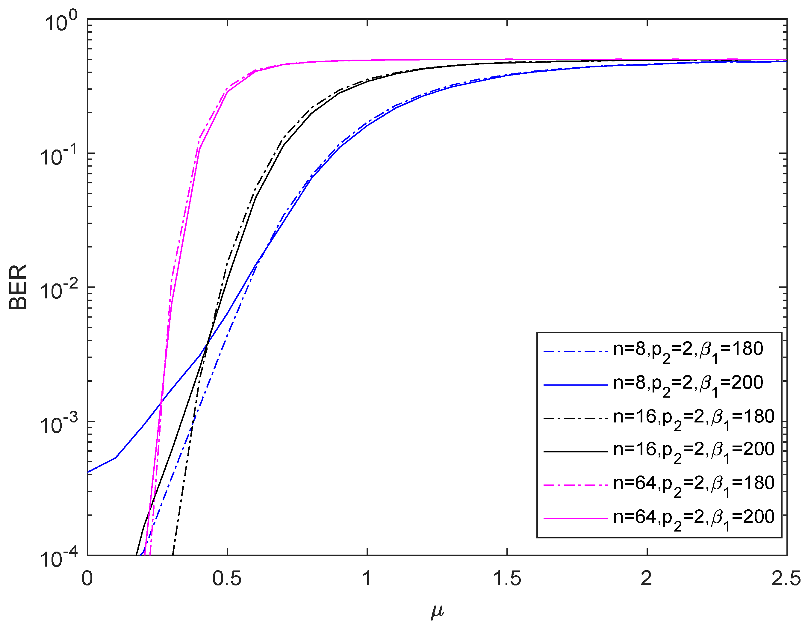
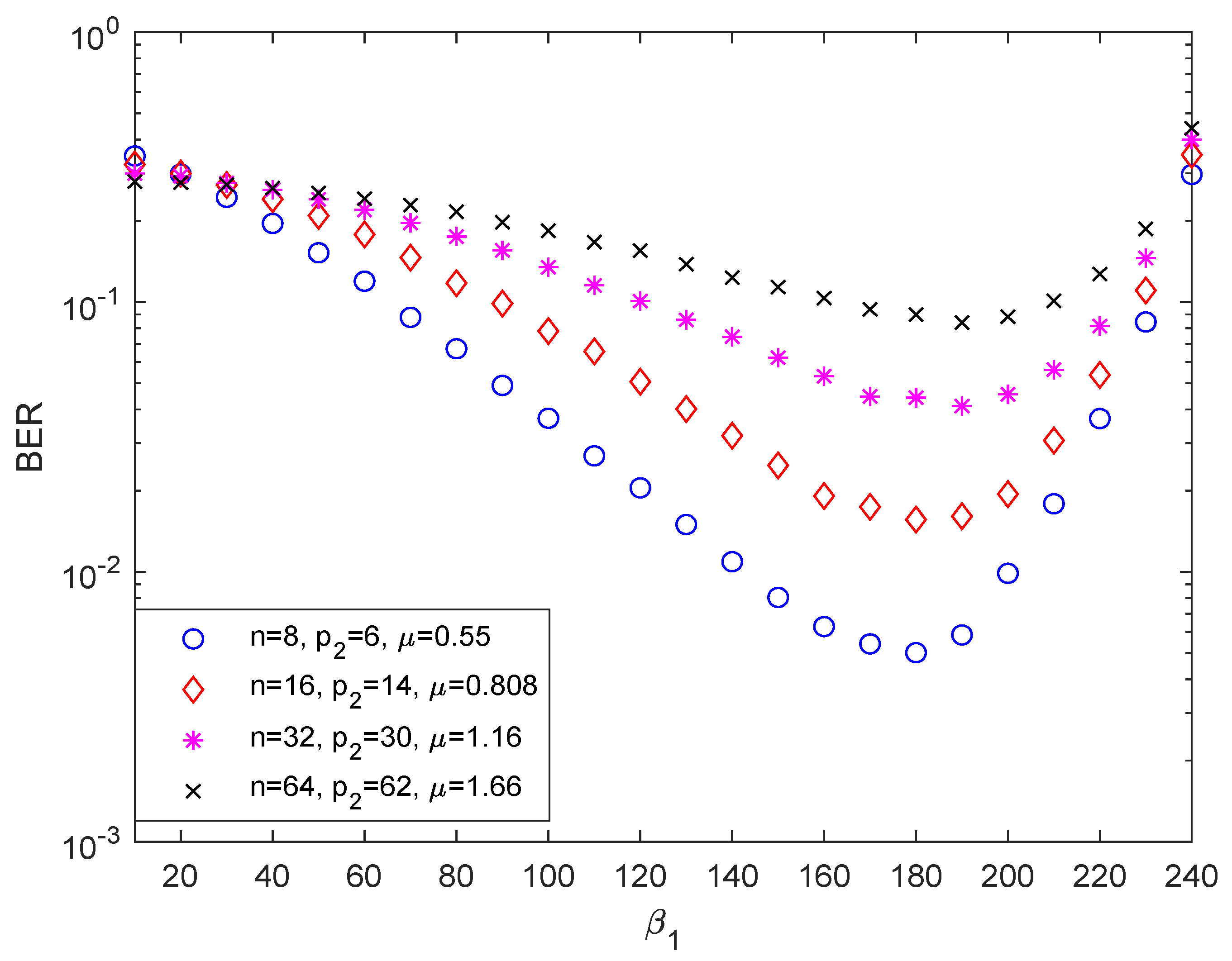
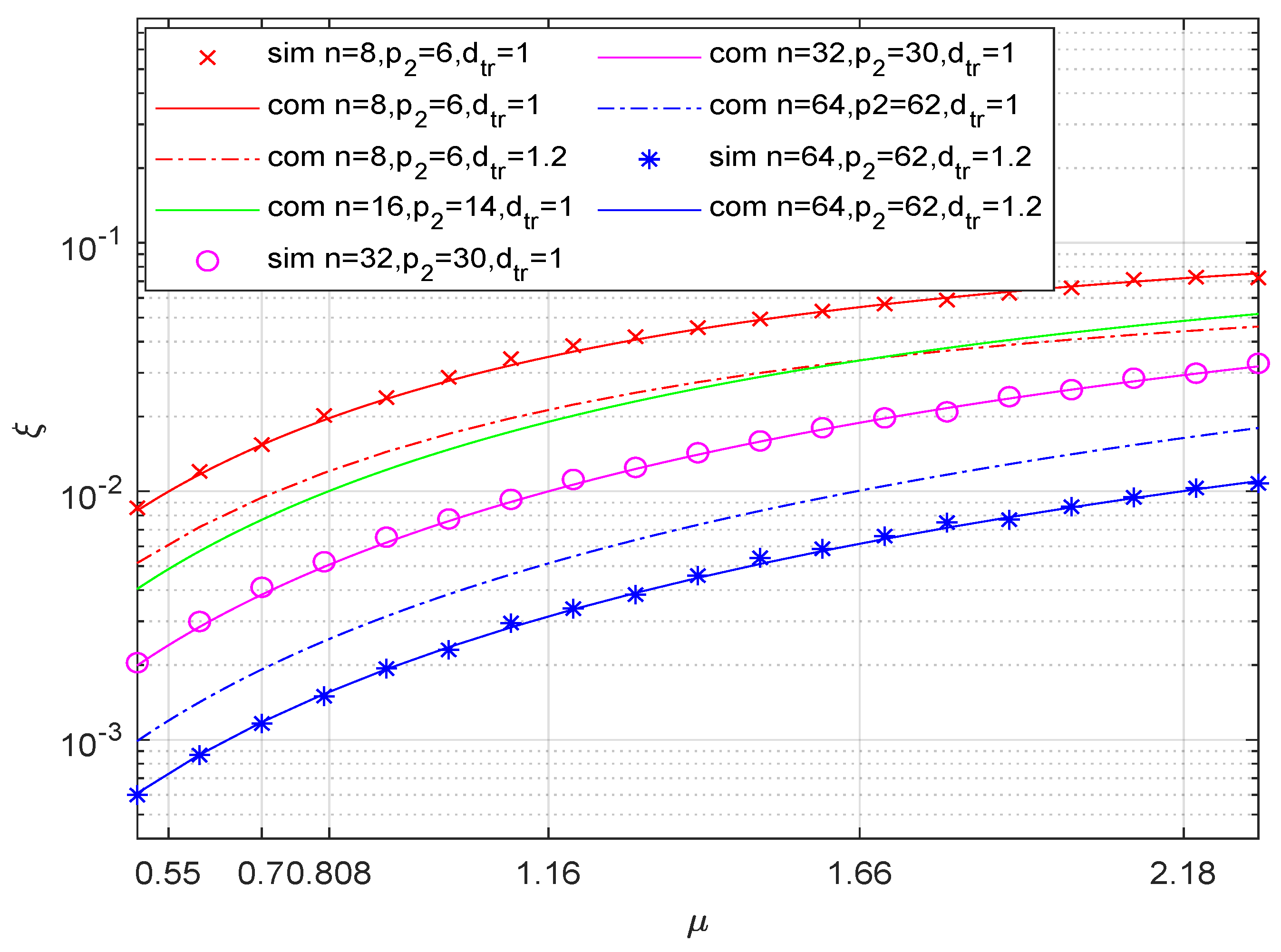
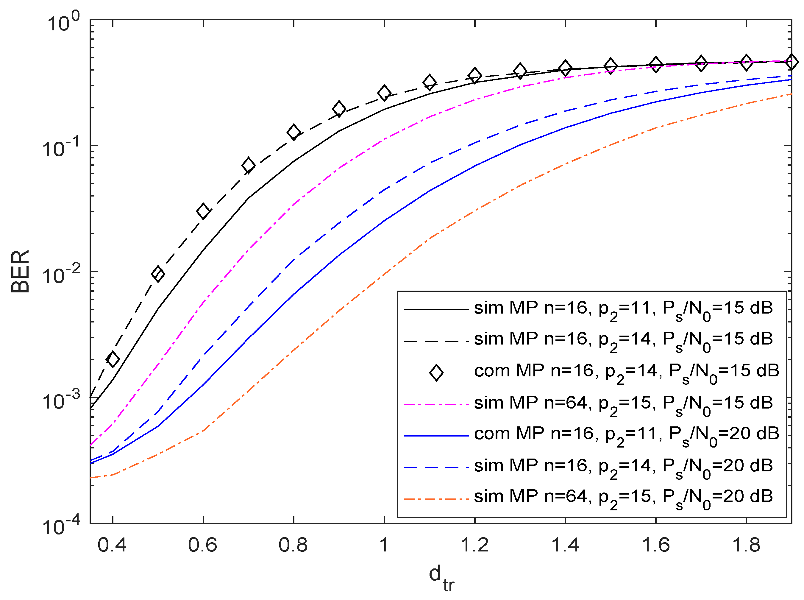
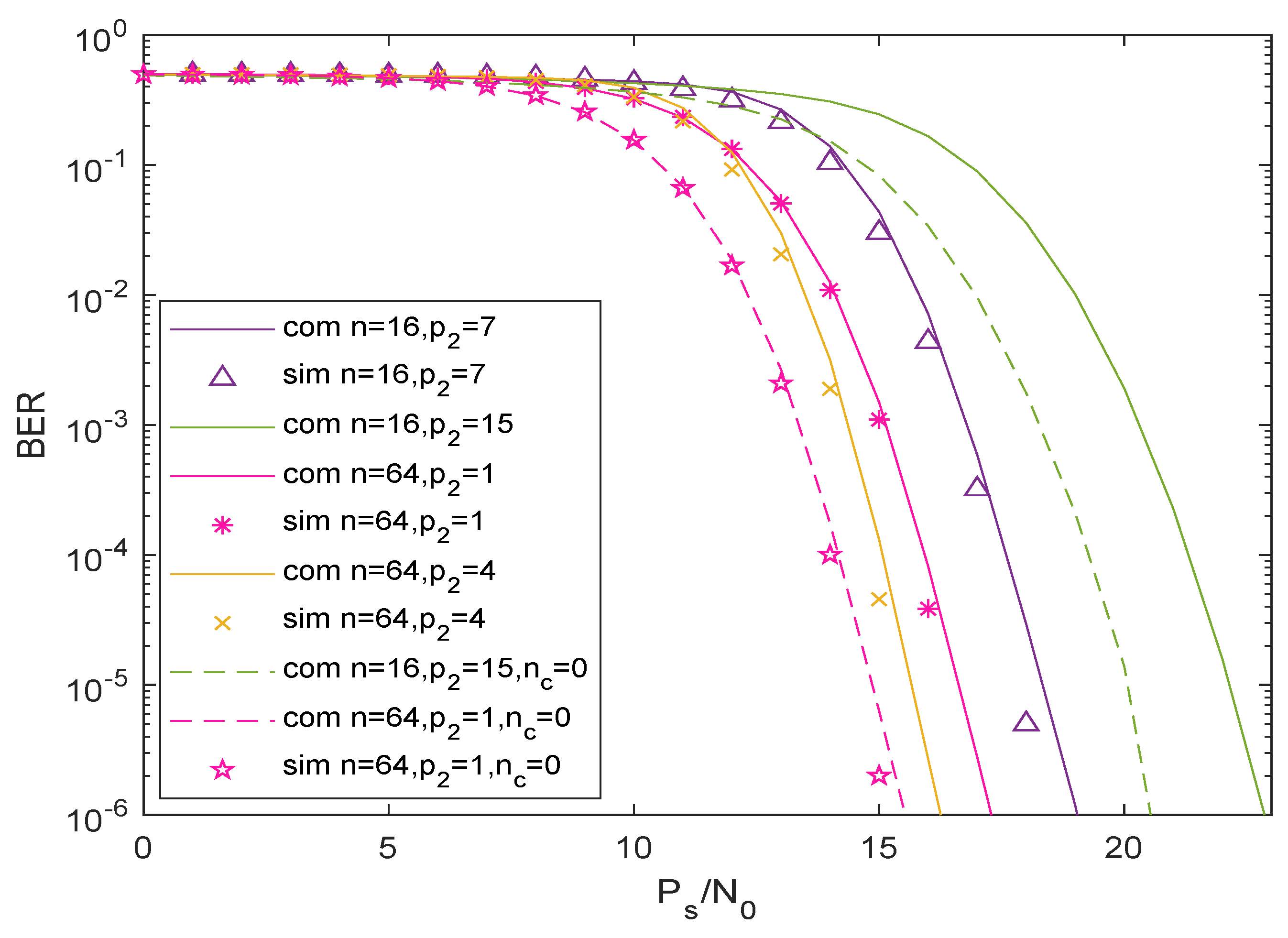
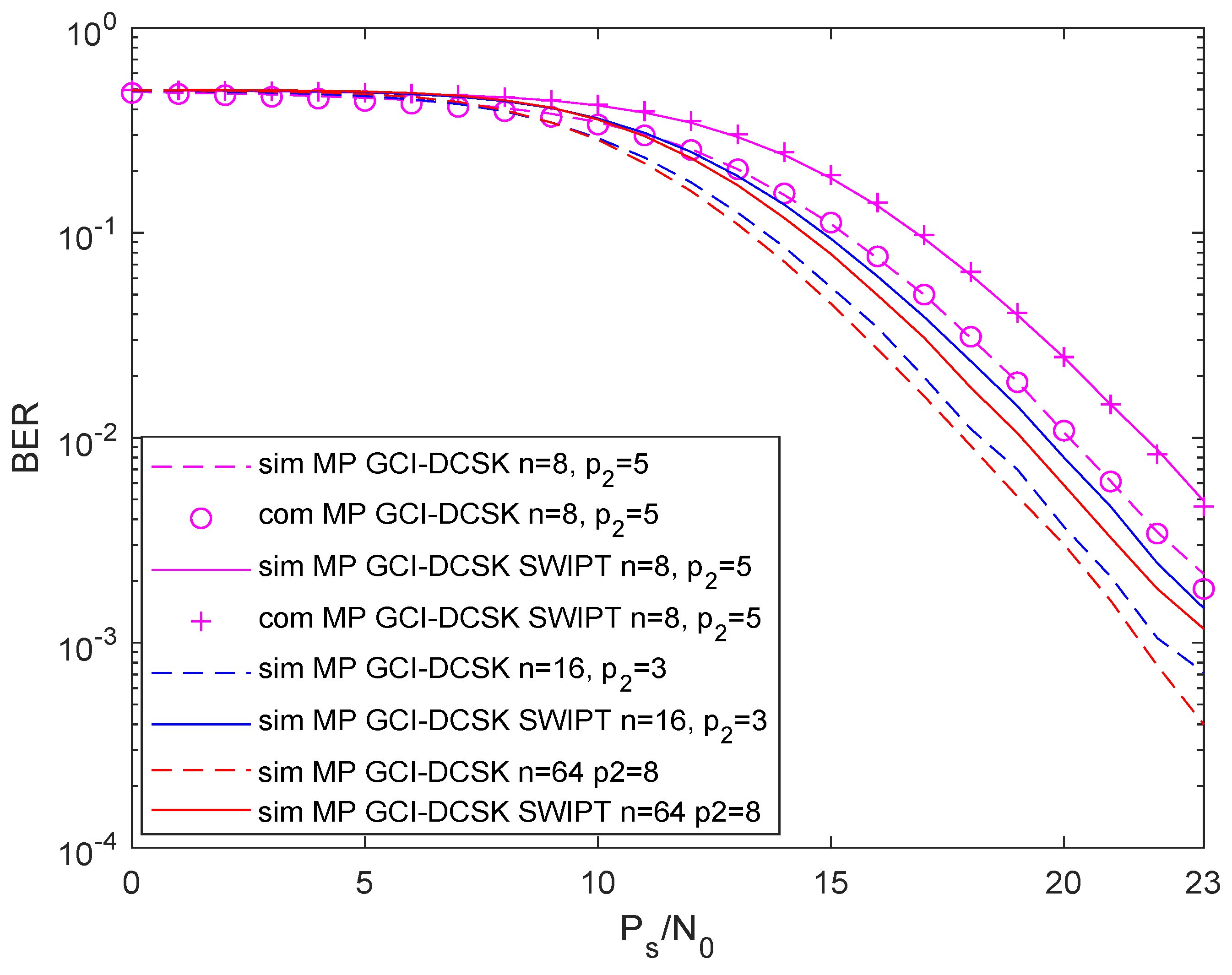
4. Numerical Results and Discussions

In this paper, the chaotic system chooses the logistic map and sets the spreading factor to 240. In simulations, P s is set to 1 Watt (W) [15,19], and the path loss factor m is set to 2.7 for propagation in urban cellular networks [19,23]. It is also assumed that N 0 , p = N 0 and N 0 , c = 0.5 N 0 , p . For a multipath Rayleigh fading channel, three paths ( L = 3 ) are considered, which have equal average power gain as E [ α 1 2 ] = E [ α 2 2 ] = E [ α 3 2 ] = 1 / 3 , with different time delays τ 1 = 0 , τ 2 = 2 T c and τ 3 = 5 T c . In the following figures, ‘com’, ‘sim’, and ‘MP’ represent the analytical BER, the simulation BER, and BER under Rayleigh fading channel, respectively.
To achieve better BER and harvest enough energy, the value of μ and β 1 should be optimized. To achieve the impacts of μ and β 1 on BER, either of them is fixed to obtain the effect of the other one on BER. Figure 2 shows the BER performance of GCI-DCSK SWIPT scheme changes along with μ over AWGN channel with P s / N 0 = 18 dB and fixed β 1 . It shows that the performance of BER degrades as μ increases. Because as μ increases, the energy of the inactive carrier increases which is adverse to BER. However, as mentioned in Section 3.3, μ should be larger than the optimal value to harvest enough energy. Figure 3 shows the BER performance of GCI-DCSK SWITP scheme changes along with β 1 setting P s / N 0 = 18 dB and μ fixed. With β 1 increasing, the BER increases after initially decreasing, and the minimum value of BER is obtained at β 1 = 180 . Hence, β 1 is set to 180 during the simulation for better BER.
Based on the above analysis, putting β 1 = 180 into Formula (32), the optimal value of μ is achieved. As shown in Figure 4, with P s / N 0 being 40 dB, β 1 being 180, and μ being the optimal value, the scheme is self-sufficient. Moreover, if d t r increases, the optimal value of μ increases to overcome the impact of more path loss.
Figure 5 shows the BER of GCI-DCSK SWIPT changes along with d t r over a multipath Rayleigh fading channel. It shows that the BER gets worse with the increase of d t r for different cases because when the distance between the transmitter and receiver increases, the probability of correct reception decreases due to the influence of increasing path loss.
The analytical and simulation results for GCI-DCSK SWIPT over AWGN and Rayleigh fading channels are shown in Figure 6 and Figure 7, respectively. The results show that the analytical results match well with the simulation results in different cases, which demonstrates the accuracy of the analytical BER expressions. To analyze the impact of conversion noise on BER performance, the curves without conversion noise are plotted and labeled as n c = 0. Obviously, both cases of n = 16 , p 2 = 15 and n = 64 , p 2 = 1 degrades by about 2 dB compared with the corresponding cases with n c = 0 over both AWGN and Rayleigh fading channels. The deterioration of 2 dB is caused by conversion noise. In particular, when the number of active carriers is 1 or n 1 GCI-DCSK SWIPT becomes conversion noise-aware CI-DCSK SWIPT. It can be clearly observed in the two figures that when n selects 16, both cases of p 2 = 7 and p 2 = 11 outperform the case of p 2 = 15 not only in BER performance but also in SE. In addition, with n = 64 , the case of p 2 = 4 outperforms the case of p 2 = 1 in BER performances and EE. Thus, some cases of GCI-DCSK SWIPT own better BER performance than conversion noise-aware CI-DCSK SWIPT, and a higher SE or EE is obtained at the same time. In addition, taking both path loss and conversion noise into consideration, GCI-DCSK SWIPT is still self-sustainable with good BER performance.
Figure 8 shows the comparison between GCI-DCSK SWIPT and GCI-DCSK with the same conversion noise over Rayleigh fading channel. GCI-DCSK achieves nearly 2 dB performance gain over GCI-DCSK SWIPT with the same configurations of p 1 and n because only the first part of chips ( β 1 ) are used for decoding in GCI-DCSK SWIPT. However, GCI-DCSK SWIPT can provide the function of energy harvest.

5. Conclusions

This paper proposes a GCI-DCSK SWIPT scheme, which is not only more flexible in selecting both the number of index bits and active carriers, but also more practical in considering path loss and conversion noise compared with the CI-DCSK SWIPT schemes. In the scheme, energy-adjustable noise-like signals will be transmitted through inactive carriers and harvested at the receiver. The analytical formulas of BER over AWGN and multipath Rayleigh fading channels are derived, which match very well with the simulation results. Moreover, the optimizations of BER and the harvested energy are introduced. Though the path loss and the conversion noise worsen the BER and reduce the harvested energy of the scheme, GCI-DCSK SWIPT is still self-sufficient with relatively good BER performance by careful design. By adjusting p 2 , some cases of GCI-DCSK SWIPT outperform conversion noise-aware CI-DCSK SWIPT in BER. Moreover, it is obvious that GCI-DCSK SWIPT offers more flexibility in EE and SE compared to conversion noise-aware CI-DCSK SWIPT.

Author Contributions

Conceptualization, M.Z. and G.C.; methodology, M.Z. and G.C.; software, M.Z. and G.C.; validation, M.Z. and G.C.; Drafting, M.Z.; proof reading and experimental analysis, M.Z., G.C., B.Y. and C.Y. All authors have read and agreed to the published version of the manuscript.

Funding

This work was funded in part by the National Natural Science Foundation of China under grant No. 62062025, in part by Guizhou Science and Technology Department Foundation grant No. ZK[2021]302.

Institutional Review Board Statement

Not applicable.

Informed Consent Statement

Not applicable.

Data Availability Statement

Not applicable.

Conflicts of Interest

The authors declare no conflict of interest.

References

  1. Kennedy, M.; Kolumban, G.; Kis, G.; Jako, Z. Performance evaluation of FM-DCSK modulation in multipath environments. IEEE Trans. Circuits Syst. I Fundam. Theory Appl. 2000, 47, 1702–1711. [Google Scholar] [CrossRef] [Green Version]
  2. Chong, C.C.; Yong, S.K. UWB Direct Chaotic Communication Technology for Low-Rate WPAN Applications. IEEE Trans. Veh. Technol. 2008, 57, 1527–1536. [Google Scholar] [CrossRef]
  3. Kolumban, G.; Kennedy, M.; Chua, L. The role of synchronization in digital communications using chaos. I. Fundamentals of digital communications. IEEE Trans. Circuits Syst. I Fundam. Theory Appl. 1997, 44, 927–936. [Google Scholar] [CrossRef] [Green Version]
  4. Sui, T.; Feng, Y.; Jiang, Q.; Liu, F.; Zhang, T. Design and Analysis of a Short Reference Orthogonal Double Bit Rate Differential Chaotic Shift Keying Communication Scheme. Electronics 2022, 11, 2020. [Google Scholar] [CrossRef]
  5. Jia, Y.Q.; Jiang, G.P.; Yang, H.; Yu, B.; Du, M.D. Design and Performance Analysis of a Multi-Carrier M-Ary DCSK System with Multilevel Code-Shifted Modulation Based on Fractional-Order Chaos. Electronics 2021, 10, 2343. [Google Scholar] [CrossRef]
  6. Başar, E.; Aygölü, U.; Panayırcı, E.; Poor, H.V. Orthogonal Frequency Division Multiplexing with Index Modulation. IEEE Trans. Signal Process. 2013, 61, 5536–5549. [Google Scholar] [CrossRef]
  7. Liu, S.; Chen, P.; Chen, G. Differential Permutation Index DCSK Modulation for Chaotic Communication System. IEEE Commun. Lett. 2021, 25, 2029–2033. [Google Scholar] [CrossRef]
  8. Xu, W.; Tan, Y.; Lau, F.C.M. Design and Optimization of Differential Chaos Shift Keying Scheme with Code Index Modulation. IEEE Trans. Commun. 2018, 66, 1970–1980. [Google Scholar] [CrossRef]
  9. Cai, G.; Fang, Y.; Wen, J.; Mumtaz, S.; Song, Y.; Frascolla, V. Multi-Carrier M-ary DCSK System With Code Index Modulation: An Efficient Solution for Chaotic Communications. IEEE J. Sel. Top. Signal Process. 2019, 13, 1375–1386. [Google Scholar] [CrossRef]
  10. Cheng, G.; Chen, X.; Liu, W.; Xiao, W. GCI-DCSK: Generalized Carrier Index Differential Chaos Shift Keying Modulation. IEEE Commun. Lett. 2019, 23, 2012–2016. [Google Scholar] [CrossRef]
  11. Cai, G.; Fang, Y.; Chen, P.; Han, G.; Cai, G.; Song, Y. Design of an MISO-SWIPT-Aided Code-Index Modulated Multi-Carrier M-DCSK System for e-Health IoT. IEEE J. Sel. Areas Commun. 2021, 39, 311–324. [Google Scholar] [CrossRef]
  12. Cai, X.; Xu, W.; Hong, S.; Wang, L.; Zhang, L. General Carrier Index Aided Dual-Mode Differential Chaos Shift Keying with Full Mapping: Design and Optimization. IEEE Trans. Veh. Technol. 2021, 70, 11665–11677. [Google Scholar] [CrossRef]
  13. Miao, M.; Wang, L.; Katz, M.; Xu, W. Hybrid Modulation Scheme Combining PPM with Differential Chaos Shift Keying Modulation. IEEE Wireless Comm. Lett. 2019, 8, 340–343. [Google Scholar] [CrossRef] [Green Version]
  14. Varshney, L.R. Transporting information and energy simultaneously. In Proceedings of the 2008 IEEE International Symposium on Information Theory, Toronto, ON, USA, 6–11 July 2008; pp. 1612–1616. [Google Scholar]
  15. Qian, M.; Cai, G.; Fang, Y.; Han, G. Design of Link-Selection Strategies for Buffer-Aided DCSK-SWIPT Relay System. IEEE Trans. Commun. 2020, 68, 6023–6038. [Google Scholar] [CrossRef]
  16. Mukherjee, P.; Psomas, C.; Krikidis, I. Differential Chaos Shift Keying-Based Wireless Power Transfer with Nonlinearities. IEEE J. Sel. Top. Signal Process. 2021, 15, 1185–1197. [Google Scholar] [CrossRef]
  17. Cheng, G.; Xu, W.; Chen, C.; Wang, L. SWIPT Schemes for Carrier Index Differential Chaos Shift Keying Modulation: A New Look at the Inactive Carriers. IEEE Trans. Veh. Technol. 2019, 68, 2557–2570. [Google Scholar] [CrossRef]
  18. Yang, H.; Tang, W.K.S.; Chen, G.; Jiang, G.P. Multi-Carrier Chaos Shift Keying: System Design and Performance Analysis. IEEE Trans. Circuits Syst. I 2017, 64, 2182–2194. [Google Scholar] [CrossRef]
  19. Nasir, A.A.; Zhou, X.; Durrani, S. Relaying Protocols for Wireless Energy Harvesting and Information Processing. IEEE Trans. Wirel. Commun. 2013, 12, 3622–3636. [Google Scholar] [CrossRef] [Green Version]
  20. Wang, L.; Cai, G.; Chen, G.R. Design and Performance Analysis of a New Multiresolution M-Ary Differential Chaos Shift Keying Communication System. IEEE Trans. Wirel. Comm. 2015, 14, 5197–5208. [Google Scholar] [CrossRef]
  21. Huang, T.; Wang, L.; Xu, W.; Lau, F.C. Multilevel code-shifted differential-chaos-shift-keying system. IET Comm. 2016, 10, 1189–1195. [Google Scholar] [CrossRef] [Green Version]
  22. Sun, C.; Yang, C. Energy-Efficient Hybrid One- and Two-Way Relay Transmission. IEEE Trans. Veh. Technol. 2013, 62, 3737–3751. [Google Scholar] [CrossRef]
  23. Meyr, H.; Moeneclaey, M.; Fechtel, S.A. Digital Communication Receivers, Synchronization, Channel Estimation, and Signal Processing; Proakis, J.G., Ed.; Wiley Series in Telecommunications and Signal Processing; Wiley: Hoboken, NJ, USA, 1998. [Google Scholar]
Figure 1. Block diagram of the GCI-DCSK SWIPT scheme.
Electronics 11 02406 g001
Figure 2. BER performance of GCI-DCSK SWIPT changes along with μ over AWGN channel with P s / N 0 = 18 dB.
Electronics 11 02406 g002
Figure 3. BER performance of GCI-DCSK SWIPT changes along with β 1 over AWGN channel with P s / N 0 = 18 dB.
Electronics 11 02406 g003
Figure 4. The ratio of the harvested energy to the transmitted energy changes along with μ for GCI-DCSK SWIPT at d t r = 1 and d t r = 1.2 , where β 1 = 180 and P s / N 0 = 40 dB.
Electronics 11 02406 g004
Figure 5. BER performance of GCI-DCSK SWIPT changes along with d t r over a multipath Rayleigh fading channel, where P s / N 0 = 15 dB and P s / N 0 = 20 dB.
Electronics 11 02406 g005
Figure 6. Simulations and analytical BER performance of GCI-DCSK SWIPT over AWGN channel with d t r = 1 .
Electronics 11 02406 g006
Figure 7. Simulations and analytical BER performance of GCI-DCSK SWIPT over multipath Rayleigh fading channel with d t r = 1 .
Electronics 11 02406 g007
Figure 8. BER performance of GCI-DCSK SWIPT compared to GCI-DCSK over a multipath Rayleigh fading channel.
Electronics 11 02406 g008
Table 1. The formulas of EE and SE for the four systems.
ModulationCI-DCSK1 SWIPTCI-DCSK2 SWIPTGCI-DCSKGCI-DCSK SWIPT
SE p 1 + 1 n + 1 p 1 + n 1 n + 1 p 1 + p 2 n + 1 p 1 + p 2 n + 1
EE p 1 + 1 2 + μ ( n 1 ) E c v p 1 + n 1 ( n + μ ) E c v p 1 + p 2 ( p 2 + 1 ) E c v p 1 + p 2 P s [ p 2 + 1 + μ 2 ( n p 2 ) ] E c v
Publisher’s Note: MDPI stays neutral with regard to jurisdictional claims in published maps and institutional affiliations.

