Article

Improvement of the Coupling of Renewable Sources through Z-Source Converters Based on the Study of Their Dynamic Model

by
Enrique Lanagran
1,
María Victoria Ortega
1,
Manuel Ortega
1,
Juan Pedro Roa
1 and
Pablo García-Triviño
2,*
1
Higher Technical School of Linares, University of Jaén, 23700 Linares, Spain
2
Higher Technical School of Engineering of Algeciras, University of Cadiz, 11202 Algeciras, Spain
*
Author to whom correspondence should be addressed.
Electronics 2022, 11(13), 2074; https://doi.org/10.3390/electronics11132074
Submission received: 13 May 2022 / Revised: 10 June 2022 / Accepted: 28 June 2022 / Published: 1 July 2022
(This article belongs to the Special Issue Feature Papers in Power Electronics)

Abstract

:
The classical coupling of renewable energy sources greatly limits the coupling power and the output voltage of the coupled sources. Moreover, it does not eliminate the randomness of the sources. In this work a renewable sources coupling with high randomness is obtained by series connection of the output terminals of Z-source converters. To achieve the coupling, the stationary and dynamic models of a Z-source-based converter have been studied. With the results of the stationary model, the converter behavior has been evaluated as a function of its parameters and a method for calculating the Z-network parameters has been implemented. Moreover, with the dynamic model a controller has been designed for all the converters. The main contributions of this work are the coupling of the sources, the stationary and dynamic models obtained and their analysis. The coupling achieves a stable supply avoiding the sources’ randomness reaching the load. A system composed of a wind turbine, a set of photovoltaic panels and two groups of batteries has been modeled. To study the system behavior and the supply quality, several aggressive tests have been forced and experimental evidence has also been provided.

1. Introduction

Renewable energy sources are increasingly being used around the world. Some of these are not directly compatible with the electricity grid, as is the case with fuel cells [1,2] and PV systems [3,4]. These sources produce energy in the form of DC that can be stored in batteries and used later in AC form using inverters [5,6]. In DC, more and more often voltage changes are necessary, for which DC converters are required [7,8]. Special features are also created that need DC-DC and DC-AC multi-task converters [7]. In addition, coupling renewable energy sources of different types and with different characteristics is a necessity and this situation requires specific design of converters to cover specific objectives [9].
Among the DC-DC converters, there are several topologies and several types of techniques that can be distinguished and among them the classic ones stand out: voltage-fed DC-DC converters which usually need high frequency transformers [10,11,12], current-fed DC-DC converter with elevator and reducer modes [13]. There are many switching techniques, but the goal is to lose as little energy as possible in the switching of the active elements using a smooth switching technique [14]. A mixture of fed-current and fed-voltage topologies with smooth switching have been integrated into a single unidirectional converter [14]. Some topologies have also been proposed for high-voltage applications seeking to obtain a large voltage gain [15,16]. Impedance source-based converters are one of the most promising techniques. This topology was introduced in [17] and since then it has been used in inverters [18]. The Z-source can regulate the DC bus voltage in inverters, being its switching technique compatible with that of most techniques used for inverters [19,20]. Making modifications on the Z-source circuit, the qZ-source is obtained as can be seen in [21]. Both circuits are very similar but have some differences in their operation: the Z-source has a higher step-up voltage gain; the qZ-source converters suffer from a lower voltage stress on their components than those of Z-source. The qZ-source has also been used in inverters [22]. In [23], a family of DC-DC converters with high step-up gain is presented. Most works about renewable energy management require converters, and especially DC ones [24,25], converters are normally treated as ideal elements, not taking into account the behavior of the converters integrated in the microgrid. This does not model the real behavior of any converter and the actual results may be very different from those studied theoretically.
Renewable energy sources generate different voltages with associated random disturbances that are difficult to control. Nevertheless, electrical grids need a stable voltage that does not depend on the sources’ randomness. Currently, structures that eliminate this problem are in an incipient state, especially with small and medium power sources for residential use. In [26,27], hierarchical control in DC microgrids and a review of power converters for microgrids with classical structures are presented.
The contribution of this paper focuses on a new configuration to improve the classical structures, where batteries and renewable energy sources are connected through converters with their outputs in series, as shown below. The design of this structure is obtained from studies of the stationary and dynamic model of a Z-source converter. With the stationary model, the behavior of the converter can be predicted as a function of its design parameters, optimizing the converters of each source or battery to be coupled in the branch.
With the dynamic model, the design of the converter controller is obtained.
The final objective is to improve the renewable sources coupling by synchronizing all the converters of the generating branch through a single controller, avoiding the sources’ randomness reaching the load. Obtaining a stable and quality supply independent of the sources’ randomness. This requires a proper design of the controller and the converters.
With the results obtained, four converter models have been designed to couple two batteries, a wind turbine and a set of solar panels. The controller has also been designed to synchronize the four converters when they work in step-up mode.

2. Architecture and Operation of the Converter

The converter power circuit on which the dynamic and stationary models have to be obtained is shown in Figure 1. All the stages of the switching process are highlighted in black. Two levels of voltage are defined: VLo (low voltage level) and VH (high voltage level). The circuit has two modes of operation: the step-up mode, which converts power from VLo to VH, and the step-down mode, which converts inversely from VH to VLo. To carry out the study, it must be started by complying with the most demanding restrictions, which are given for the step-up mode. This mode contains a process with five stages.
The state of the active elements (transistors and diodes) is identified with 1 when they are active and 0 when they are not active. The Z-network is symmetric with L1 = L2 = L, C1 = C2 = C, and every time IL1 = IL2 = IL, IC1 = IC2 = IC, is verified. The entire switching process of the converter in step-up mode is shown in Figure 2. In [7] the detailed switching process is shown.

2.1. Choice of Converters

There are many topologies of DC/DC converters and many applications for them, the converter must be searched according to the application. Among the classic topologies, the following stand out: Voltage source converters, which would not be suitable in our application, because they need a wide range of voltage regulation. Current source converters, which are more limited than other topologies in voltage gain and converted power. Converters based on high frequency transformers (HFT) could be suitable for our application, but with high voltage gains, they need a lot of copper wire and are more expensive, they are also more limited in converted power. In [12], a converter working as a battery equalizer is presented and in [13] a method of compensation of the leakage-inductor parameter based on converters (HFT) is proposed.
The Z-source has been used in inverters with very good results [18] looking for different applications such as motor control [24]. Making modifications on the Z-source obtained the qZ-source [21]. Both techniques offer high voltage gain, support wide output voltage regulation and can be configured as bidirectional using few components. They are also good candidates for coupling. Their most significant differences are: the voltage stress of Z-source converters is twice that of qZ-source converters, the voltage gain of the Z-source converters is somewhat higher than that of the qZ-source converter. However, the Z-source converter was chosen because it has an almost linear voltage response versus duty cycle variations (which greatly simplifies control), as well as having a more symmetrical structure that facilitates the integration of the converters in the branch.

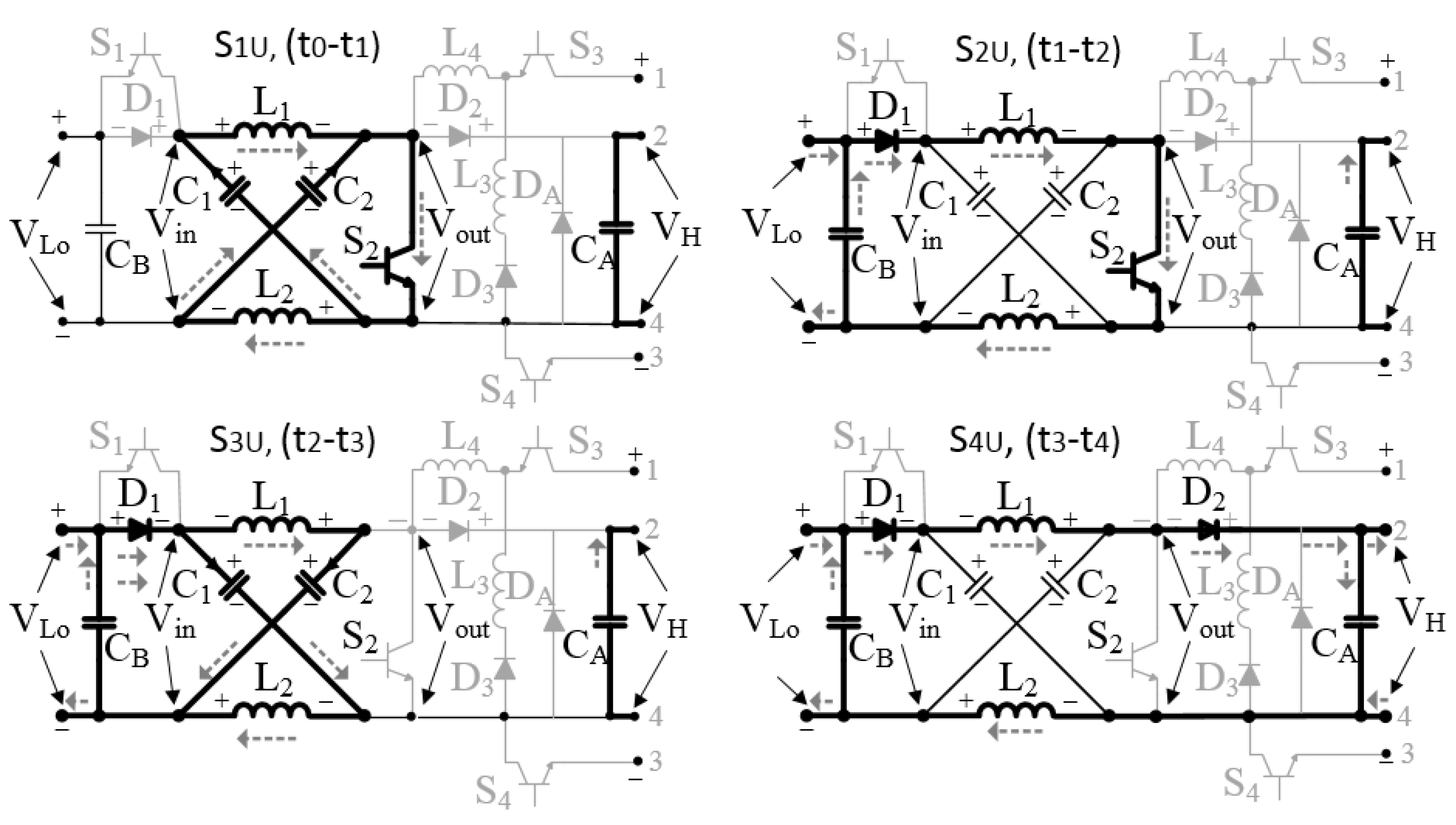
2.2. Step-Up Mode Stages

Step-up mode is the only mode involved in the coupling and is found in both bidirectional (Bc) and unidirectional (Uc) converters. Figure 1 shows the circuit stages of the used bidirectional converter. However, to highlight the step-up mode circuit, the components S3, S4, L3, L4 and D3 must be suppressed (in the figure they have been drawn in gray) and consequently the step-down mode is eliminated from the converter. Figure 1 shows the circuits highlighted in black of the first four stages. The switching process takes place in the same order in which the stages occur. The stages of each converter in step-up mode are:
Stage-S1U, (t0–t1): the following code indicates the status of the devices S1S2S3 = 010, D1D2D3 = 000, in the instant t0 S2 is turned on and the capacitors C1 and C2 are loaded with the voltage VC = V0C (initial VC of each duty cycle). At this stage, C1 and C2 discharge their energy through L1 and L2, respectively, the voltage of capacitors C1 and C2 varies from VC = V0C to VC = VLo/2. Then, L1 and L2 are energized by the capacitors, in Figure 2a, all the variables of this stage can be observed between the coordinates t0 and t1. Similarly, the variables of the remaining stage s can be seen in their corresponding coordinates.
Stage-S2U, (t1–t2): S1S2S3 = 010, D1D2D3 = 100. The inductors L1 and L2 are connected in series and are energized from the source through D1, being satisfied in this stage VC = VLo/2, Vout = 0 and Vin = VLo. The energizing of L1 and L2 from the Z-source starts at t1, and it starts with a high value of IL1 and IL2. This value has been obtained by discharging C1 and C2 on L1 and L2, respectively (this is the key of the Z-source when it is working in step-up mode).
Stage-S3U, (t2–t3): S1S2S3 = 000, D1D2D3 = 100, the disconnection of S2 occurs in t2, and Vout = VLo/2 = VC2 = VC1 is verified, see Figure 2a. In the interval t2 < t < t3, IL1 = IC1 and IL2 = IC2 are met, then the capacitors’ recharge happens from time t2 to time t3, when the condition VC2 = VC1 = V0C is verified, being the voltage V0C maintained until the beginning of the next cycle. When S2 is deactivated, two branches formed by L1, C2 and L2, and C1, and each branch is connected in parallel (seen from Vin), so that L1 charges C2 and L2 charges C1, see Figure 1. Moreover, due to circuit configuration change at t2, the current ID1 experiences a strong increase fulfilling ID1 = IL1 + IL2. Besides, Vout raises its value from zero at t2 to Vout = VC1 + VL1 = VC2 + VL2 at time t3.
Stage-S4U, (t3–t4): S1S2S3 = 000, D1D2D3 = 110. Vout becomes slightly larger than VH at t3, consequently D2 begins to conduct. Then, the energy is transferred from the battery and the inductors L1 and L2 to the capacitor CA. After, this energy is supplied to the load throughout the whole period. At this stage, the conditions VC1 = VC2 = V0C and IC1 = IC2 = 0 are verified, and then the contribution of energy to the load is made by L1, L2 and the battery, see Figure 2a between times t3 and t4.
Stage-S5U, (t4–t0): S1S2S3 = 000, D1D2D3 = 000. At t4 the inductors have discharged all their energy on CA and the current flow has been extinguished in D1 and D2. Moreover, it is verified that Vin = Vout = VC1 = VC2 = V0C. This situation is kept until the beginning of the next cycle. This converter has a discontinuous conduction mode, thus this stage is necessary. Its duration depends on the value of the duty cycle D, during this period no current flows through any of its devices. This stage has not been represented in Figure 1. During this stage, current does not flow through any device, only the discharge of the CA capacitor on the load is taking place.
The largest possible duty cycle is D = 0.9 T (T being the duty cycle). If D > 0.9T, then the converter can work in continuous conduction, circulating very high currents through the Z-network without ever extinguishing (the Z-network can be destroyed). For safety reasons the maximum duty cycle is limited to Dmax < 0.8 T.
The step-down mode does not intervene in the coupling, it is only in the bidirectional converters and works in reverse of the step-up mode. The step-down mode only affects the battery converters when it has to store excess energy from the sources. Therefore, this subject is treated with less depth; its commutation is shown in Figure 2b. The inductance L4 has the mission to adapt the step-down gain, to convert the voltage of the DC bus (Vdc = VH) to the voltage of the battery (VLo = VB). The inductance L4 is calculated after the design of all the step-up mode parameters.

3. Converter Analysis

Figure 1 shows the four-stage circuits of the step-up mode. In the switching process, five stages can be distinguished. Each of them is identified with a variable that represents the duration of the stage with respect to the total period T. All variables depend on the duty cycle D and the switching period T. Between these stages, there are several relationships that have been taken from experimental tests and are shown in (1).
Stage-S1U ,   ( t 0 t 1 )   α = 0.13 D × T ;   Stage-S2U ,   ( t 1 t 2 ) β = 0.86 D × T Stage-S3U ,   ( t 2 t 3 )   γ = 0.11 D × T ;   Stage-S4U ,   ( t 3 t 4 )   δ = 0.05 D × T Stage-S5U ,   ( t 4 t 0 )   λ = ( 1 1.16 D ) × T = ( 1 ( 1 + γ + δ ) D ) T

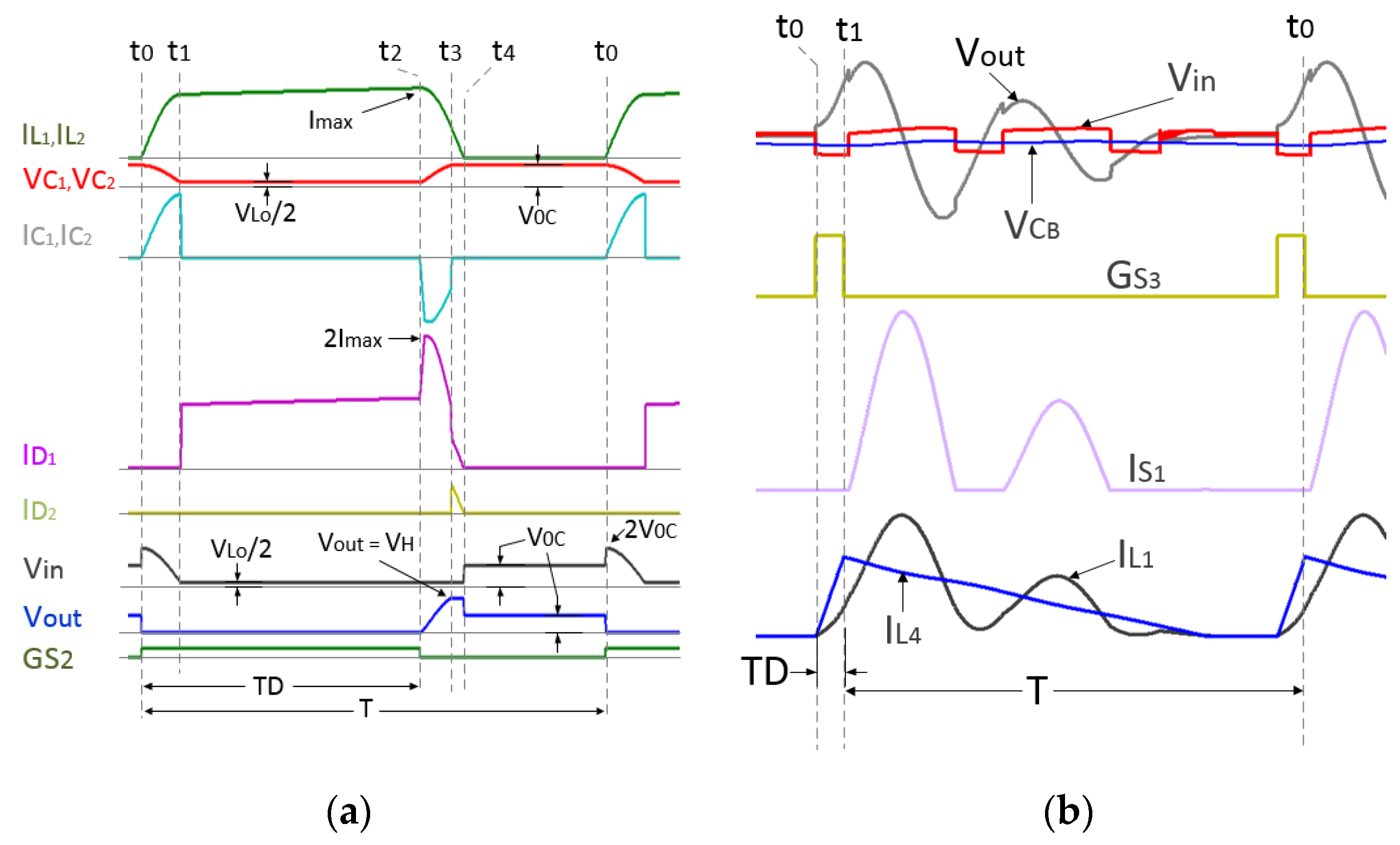
Step-Up Mode Equations

In order to obtain the equations, the parameters that have a lesser effect on the final solution, such as the resistance of the capacitors, are not taken into account. In the study, transistors are considered ideal.
Stage-S1U, (t0–t1). The converter circuit of this stage can be seen in Figure 1. Only the operation of the Z-network has been highlighted. In Equation (2), the current in the IL inductance of the Z-network is related to the voltage in the VC capacitors, in (3) the variation of the voltage in the Z-network is evaluated. For this reason the value of the converters’ output voltage VH has been taken into account, which in this stage is related to the capacitors’ voltage C1 and C2. In (4), the voltage variation in the output capacitor CA is valuated as a function of the load current, in the remaining stages this evaluation is also obtained.
L d I L d t = V C R L I L
C d V C d t = V H 2 × α D C
C A d V H d t = V H R L o a d
Stage-S2U, (t1–t2). D1 starts driving and the circuit changes. The following equations can be proposed. In (5), the inductors’ current variation L1 and L2 are studied, they are fed from the battery with a voltage VLo/2, see Figure 1. The voltage variations on capacitors C1 and C2 are evaluated with (6), these are also evaluated in the remaining stages.
L d I L d t = V L o 2 R L I L
C d V C d t = 0
C A d V H d t = V H R L o a d
Stage-S3U, (t2–t3). S2 is disconnected and the Z-network capacitors C1 and C2 start a recharge process. The recharge energy is obtained from the source and the inductors. In (8), the IL1 and IL2 variations are evaluated according to all involved variables and in (9) the recharge process of C1 and C2 is modeled.
L d I L d t = V C R L I L + V L o
C d V C d t = I
C A d V H d t = V H R L o a d
Stage-S4U, (t3–t4). The voltage of the capacitors C1 and C2 after the recharging process reached their maximum value, then the battery and the inductors L1 and L2 begin the process of transferring energy to the capacitor CA and the load. This situation can be modeled with the following equations.
L d I L d t = R L I L V H V L o 2
C d V C d t = 0
C A d V H d t = 2 I L V H R L o a d
Stage-S5U, (t4–t0). During this stage, all the variables within the Z-network remain constant and the only voltage that varies is that of the capacitor CA (represented in 16), which feeds the load during the whole period. Equations (14) and (15) represent the inductors’ current variations L1 and L2 and the capacitors’ voltage variations C1 and C2, respectively.
L d I L d t = 0
C d V C d t = 0
C A d V H d t = V H R L o a d
The switching frequency used is 10 kHz or higher and then T = dt. In addition, by introducing a switching function satisfying (SwD = D if Sw = 1) and ((1 − Sw)D = D if Sw = 0), this function activates each stage when necessary and the value of the state variables can be averaged over a switching period dt.
By introducing the switching function in the equations of the system (2)–(16), averaging throughout the whole period dt and simplifying the derivatives, the Equations (17)–(19) are obtained.
d I L d t = R I L L ( S w ( α β + γ + δ ) + ( γ δ ) ) + V C L ( S w ( α + γ ) γ ) + V H 2 L δ ( S w 1 ) + V L o L ( S w ( β 2 γ δ 2 ) + ( δ 2 + γ ) )
d V C d t = I L C ( 1 S w ) γ + V H × S W 4 D γ
d V H d t = 2 I L C A δ ( 1 S w ) + V H R l o a d C A ( S w ( α β + γ + δ + λ ) ( γ + δ + λ ) )
Taking into account that ( α + β + γ + δ + λ ) D = T , eliminating the switching function Sw and reducing, the following expressions are obtained.
d I L d t = R I L L ( α β γ δ ) D + V C L ( α γ ) D V H 2 L δ D + V L o L ( ( β 2 + γ + δ 2 ) ) D
d V C d t = V H 2 α I L γ D C
d V H d t = 2 I L C A δ D V H R l o a d C A
The steady state is obtained when the derivatives become zero, and taking into account that in the stage S1U, Vc varies from ( V H + V L o ) / 2 in t0 up to V L o / 2 in t1 and in the stage S3U, Vc varies from V L o / 2 in t2 up to ( V H + V L o ) / 2 in t3. From the expressions (20)–(22), (23) is obtained, relating all the variables in a stationary model, with which the steady-state voltage gain can be analyzed in the function of the component parameters of the converter.
V H V L o = 2 L R L o a d α 2 D + R R L o a d α β 2 D 2 + R R L o a d α 2 β D 2 + 2 L R L o a d α β D + 4 L R L o a d α γ D 2 L R α + L R l o a d α 2 D + C L R R l o a d β + 3 L R L o a d α γ D
Substituting the values α = 0.13 ,   β = 0.86 , γ = 0.11 , and δ = 0.05 , expression (24) is obtained.
V H V L o = 157,300 L R L o a d D 40,807 R R L o a d D 2 130,000 L R + 1300 L R l o a d D + 430,000 C L R R l o a d
With the expression (24), the behavior of the converter can be evaluated at steady state. Consider that the model has been created in an average value, making 1/f = T = dt.
For example, if the evolution of the gain in function of the duty cycle is studied with (24), assigning the values of the parameters L = 1.5 μH, C = 20 μF, V L o = 12 V, R L = 0.002 Ω and taking three load resistors R L o a d = 75 , 100 and 150 Ω , the three graphs shown in Figure 3a are obtained. In this figure it can be seen that the gain is higher as the loads become smaller.
If the study is performed by varying the internal resistance of the Z-network, with a load resistance of R L o a d = 85   Ω , Figure 3b is obtained, where it can be observed that the gain decreases quite a lot with the increase of the internal resistance of the Z-network. Therefore, if large step-up gains are necessary, then the Z-network must have a low internal resistance and the inductors must have few turns.
Figure 3c,d show the study of the Me evolution with respect to De, using different capacities and inductances, respectively, in the Z-network. It is obtained that the variation of the inductance values as capacitance in the Z-network have a small effect on the converter voltage gain. From the stationary model, (25) has been obtained. With this expression, the converted power PC can be found, shown in Figure 3e, where it can be observed that the converted power increases as the capacitors’ capacity values increase and the inductors’ inductance values decrease.
P C = V s ( ( C ( V H 2 4 + V L o V H 2 ) / L ) + T V L o D e max 4 L ) D e max
Consequently, the design of a Z-source converter requires a proper search of the parameters that make up the Z-network, the values of C1, C2, L1 and L2 as well as their internal resistances. This is made for obtaining the necessary gain, ensuring that the converters can convert the maximum power needed and limit the power in case of short circuit in the load. This search becomes more demanding when the converters must be coupled with their outputs in series.

4. Dynamic Model and Converter Coupling Control Strategy
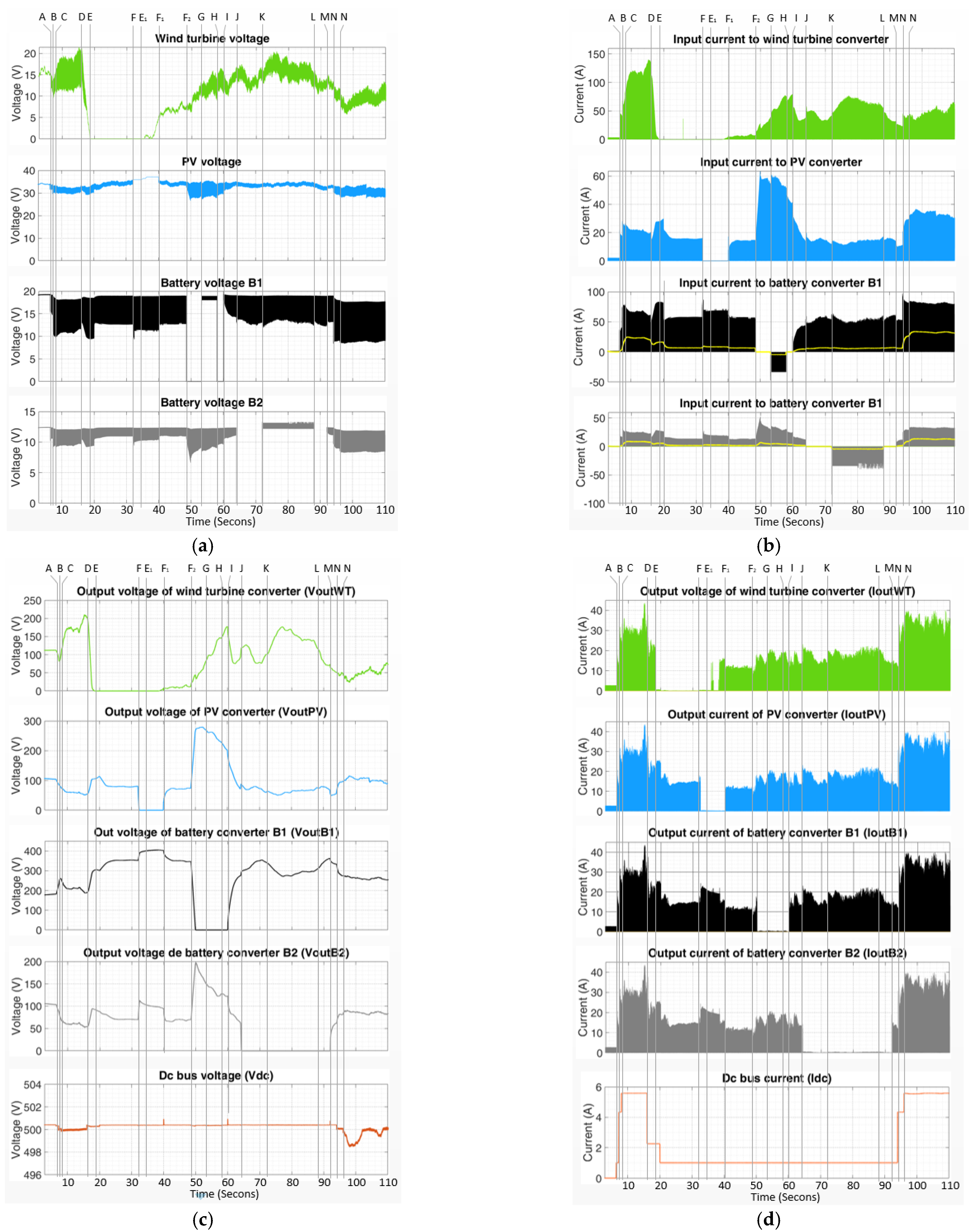
Starting from the Equations (20)–(22), the dynamic model of the system is obtained. This model permits to develop a driver for the converter. The following state variables are defined.
X 1 = I L       X 2 = V C       X 3 = V H       X ˙ 1 = d I L d t       X ˙ 2 = d V C d t       X ˙ 3 = d V H d t       u ( t ) = D
The matrices of the dynamic model are:
A = ( R L ( α + β + γ + δ ) D ¯ 1 L ( α γ ) D ¯ 1 2 L δ D ¯ γ D ¯ C 0 1 4 2 C A δ D ¯ 0 1 R l o a d C A ) B = ( 1 L ( ( β 2 + γ + δ 2 ) ) V L o I L γ C 2 I L C A δ ) Y = ( 0 0 1 ) × ( X 1 X 2 X 3 )
Starting from the dynamic model, the transfer function of the controller can be obtained. Since four converters whose outputs are connected in series, and all four have the model shown in (26), must be controlled, each converter couples a different source and then the converters have different parameters from each other. Therefore, to design the controller, we have worked with an average transfer function, averaging the parameters of the four converters.
Taking into account the four modeled converters, the average values of the converter parameters are: VLo = 22 V (average power supply value of the source voltages), C = 3 µF, L = 18 µH, CA = 250 µF, R = 0.002 Ω, RLoad = 75 Ω (estimated average load resistance). Moreover, the eigenvalues of the switching α = 0.13, β = 0.86, γ = 0.11 and δ = 0.05, which are similar in the four converters. On the other hand, the most unfavorable working point must be taken into account with D = 0.8, and a current in the inductors that in our case has been taken from IL = 95 A. Substituting in (26), the transfer function of the converter plant of the average converter is obtained as (27).
G ( s ) = 38 × 10 3 s 2 + 2.249 × 10 8 s 2508 × 10 4 s 3 + 142.2 s 2 + 2.643 × 10 7 s + 1.043 × 10 9
C ( s ) = 175 ( s + 20 s ) ( 1 + 0.40 s ) s ( 1 + 70 s )
In the representation of the place of the roots of (27), shown in Figure 4, it can be seen that the system is stable, since it has all the poles and zeroes in the left half plane, and it presents a phase margin of 87.5 degrees and an infinite gain margin. Using MATLAB®, a PID controller was designed (which acts in the step-up mode of the four converters varying its duty cycle) as shown in (28), composed of a pole at −70, two zeroes at −40 and at −20 an integrator. Figure 4b shows the response of the system in open loop and in closed loop with the controller (28). Observing the step response, it can be verified that with the proposed controller the plant has been controlled.
As it is indicated in (29), if the classical structure of a PID is compared with (28), then the constants are obtained with the values Kp = 121.4, Ti = 0.06 and Td = 0.0063.
As the controller is very fast and there is enough margin, the value of Td can be disregarded and then the controller becomes a PI and its response is delayed a bit, but this situation is not significant. Likewise, the value of Kp can be reduced at the cost of increasing the establishment time, without a significant modification of the response.
K p ( 1 + 1 T i × s + T d × s ) = 175 ( s + 20 ) ( s + 40 ) s ( s + 70 )

5. Results

The difference between the classical coupling structure and the proposed coupling can be seen in Figure 5a,b, respectively.
The proposed system has been tested with the coupling of the models of a wind turbine, some solar panels and two batteries, all of them coupled in series through the output terminals of the four Z-source converters, and a controller that regulates the duty cycle of the four converters, see Figure 5b. For the coupling of the sources and the batteries, unidirectional and bidirectional Z-source converters are utilized, respectively.
The average dynamic model has been used for controller design. The designed converters have been tested by simulation working couples as shown in Figure 5c. The possibilities of management of the system for decision making are several (neural networks, fuzzy logic, etc.) but they are not contained in this work. The designed controller has the mission of maintaining stable Vdc by adapting the duty cycle of the four converters, in order for each source to contribute proportionally to the power demanded by the load, having the system have the capacity to work as if it were a single generation unit, taking advantage of all the energy generated. Figure 6 presents the results of the system behavior as well as its adaptive capabilities.

Design Considerations

In the coupling, a model of a three-phase wind turbine (WT) of 1000 watts without a regulator has been used, with a full bridge rectifier and a filter at the output. Its output voltage depends on the wind speed (5–26 V). The nominal power is obtained at 12 m/s, producing automatic braking at 14 m/s. Another converter is placed in the model of eight solar panels (PV), with a maximum nominal power of 410 W per panel and an output voltage of 35.9 V in conditions of maximum power. Two groups of 600 Ah batteries of 18 and 12 volts have also been modeled. For the coupling of sources, the models of the four converters as indicated in Figure 5b,c were used. Consequently, the four converters are coupled with their output terminals connected in series. Therefore, the system (converters and controller) dampens the random variations that occur in the sources, the load is not affected at any time and the tension in the DC bus Vdc remains substantially constant.
For the converters’ design that makes the integration of the sources in the generating branch, the method exposed in [7] has been considered, which has been improved with the results provided by the stationary model and the converted power expression (25). In the model, the reference voltage to obtain the voltage Vcd of the DC link has been set at 500 V. As two batteries are available, it is expected that both can support the system in case of need (if all other sources are unable to contribute). The design data for the step-up mode are shown in Table 1 and the design values assigned for the output voltage of the battery converters are: VoutB1 = VHn = 270 V and VoutB2 = VHn = 450 V. The design data of the converters coupled to preserve the voltage Vdc, close to 500 V are shown in Table 2 and Table 3.
If a source with a generated voltage range (7–15) V is to be coupled to a generator branch, for the converter design, the source power (e.g., 1000 W) and average voltage value VSn = 12 V must be considered. Likewise, the average output voltage of the converter Vout = 250 V must be defined (for this, the other sources and the most unfavorable coupling conditions must be taken into account), the maximum duty cycle in this case is De-max = 0.8 and the switching frequency in this case is set at 10 kHz. Moreover, the converter must be able to convert a little more than 1000 W, but not much more (even in case of short circuit) to protect the source.
The L and C values of the Z-network are obtained by substituting the previous data in (25). In Figure 3e, the expression (25) has been represented with the indicated above values. To couple a source of 1000 W, it can be seen that there are several L and C values that could be used. For example, if the L = 18 µH and C = 10 µH is taken, then with (24) the maximum gain obtained with these values is studied. For this objective, a load resistance Rload = 62.5 Ω is taken (resistance that consumes 1000 W fed with VH = 250 V). The only missing parameter is the inductors’ resistance R. This parameter will be calculated so that the converter has the desired gain, in this case Me = 20.86 (250/12). The value obtained is R = 71,236 µΩ. To calculate the values of It1 and It2max, the expressions (31) and (32) are used, respectively, obtaining It1 = 97.89 A and It2max = 126.78 A, these values are necessary for the design of the components.
The coils will be designed for an average current value of It1 and It2max, in this case with Imed = 112 A, inductance L = 18 µH and with internal resistance R lower than 71,236 µΩ. For this purpose, as many parallel branches as are necessary will be used.
The converters are designed with the above method and coupled as shown in Figure 5b. They add up their energies from renewable sources to obtain a quality supply. Therefore, even if the energy is produced with voltage and power disturbances, these do not reach the load. The Simulink® model is shown in Figure 5c. The converters have been modeled with a high level of accuracy to obtain quality results. Different situations have been forced in the tests to show the capabilities of the coupling.
Table 2 shows the parameters obtained for the modeling of the converters in step-up mode.
If the output voltage of the wind turbine (Figure 6a) is observed, it undergoes a large voltage oscillation that is proportional to the power generated. The coupling system allows the power generated with disturbances to reach the load without them. Observe the voltage of the bus DC Vdc in Figure 6c, where the Vdc voltage remains almost constant despite the power and voltage oscillations in the sources and changes in the demanded load.
Consequently, the expression (30) is always verified.
V d c = V o u t W T + V o u t P V + + V o u t B 1 + V o u t B 2
( I L ) t 1 = C L V H 2 + 2 V H n V S n 4
( I L max ) t 2 = I L t 1 + V S n 2 L D e max T
There are two main sources, PV and WT, and two groups of batteries with different voltages, both the sources and the batteries are coupled through the converters optimizing the energy generated and achieving a stable power supply. To show the operation of the system, tests have been forced on the model that demonstrate its robustness against variations in load as well as variations in energy production. To better understand the results and the variables’ location in the circuit, Figure 1 and Figure 6 should be observed at the same time.
In step-up mode, the control of all converters has been made with a single PID obtained in (28). In Figure 6 the results of a forced operation are shown and the designed converters’ behavior that integrate the coupling branch can be seen. Figure 6b presents the currents between the CB capacitors and the Z-source of each converter. In addition, in the battery converters the currents between the battery and the CB capacitor are also represented in yellow (so that the battery charging process can be appreciated).
In the coordinates A, B and C, three resistors of 500, 150 and 400 Ω are connected successively, and it can be seen that there is a current increase in the capacitors’ output CB in all the converters (see Figure 6b). The contribution of power to the load is unequal in each source and depends on the design of the converter of each source and of the source itself. The system can supply energy to the load using the primary source’s energy and when these do not cover the demand, some energy from the batteries is used.
Between the coordinates E and F1 there are two zones to consider (see Figure 6a): when the voltage of the wind turbine becomes zero between the coordinates E and E1 and when the total disconnection of the solar panels between F and F1 occurs. As observed in Figure 6b, in these zones the input currents to the wind turbine converter and the PV converter become zero, each one in its corresponding zone and these sources do not provide power to the load.
Moreover, in Figure 6c, it can be seen in the same coordinates (E, F1 and F, F1) that the output voltages of the PV and wind turbine converters are also zero, but the voltage in the DC bus Vdc is kept almost constant, being met at all times (30). In this case, the batteries are the ones that supply the energy demanded by the charge, when the sources do not cover the supply of the charge. Specifically in the coordinate E1, the values of the voltages are approximately VoutWT = 0 V, VoutPV = 0 V, VoutB1 = 400 V and VoutB2 = 100 V, all adding up Vdc = 500 V.
After reconnecting the PVs at the coordinate F1, battery B1 at coordinate F2 is disconnected. Due to this disconnection, as seen in Figure 6b,c, there are sharp increases in both the input current to the PV converter and the VoutPV voltage, the power that was supplied by B1 to the load is now supplied by PV. Then, between the coordinates G and H the battery B1 has been put into charge, storing energy from the primary sources. As seen in Figure 6b, the input current to the battery converter B1 is negative. Looking at Figure 6c, it can be seen that the battery that is being charged does not provide voltage to Vdc, being VoutB1 = 0 between the coordinates F2 and I. The same procedure between the J and M coordinates has also been forced on the B2 battery. If a battery is charging, it does not supply power to the branch, but it can store excess energy, while the other converters and their sources supply the load with a stable supply.
On the other hand, as seen in Figure 6d, all the output currents of the converters are equal to each other, except during the time in which the sources do not produce energy or their converters have been disconnected. This is because the Z-networks of all active converters are connected in series while the switching of each active converter takes place. For example, in the E coordinate of Figure 6d, IoutWT becomes zero (the wind turbine does not produce energy in that time), but the output currents of the other converters (IoutPV, IoutB1 and IoutB2) are equal to each other and are feeding the load. Each converter has an output capacitor labeled CA. The currents IoutWT, IoutPV, IoutB1 and IoutB2 charge this capacitor in its corresponding converter. The shape of these currents are pulses shown in Figure 6b.
Then, the bus current Idc which feeds the load (shown in Figure 6d) is continuous with very low oscillations, the output voltages VoutWT, VoutPV, VoutB1 and VoutB2 of each converter are measured at the terminals of the capacitors CA of each converter, and the sum of them produces the bus voltage Vdc, see Figure 6c. Despite the large oscillations that occur in all the Vout voltages of the converters (due to the randomness of the load and the generation), the coupling system of the sources, by means of the Z-source converters, keeps the voltage value of the DC bar Vdc nearly constant (close to 500V) and provides a quality supply at the load. After the N coordinate, there is a sharp increase in the load, but despite this, a DC bus voltage oscillation of approximately 2V can be observed, see Figure 6c, which is less than 1% of the voltage Vdc.
When the sources generate power with associated disturbances or a sudden disconnection of some source, battery or of its converters occurs and likewise when the generated power at the sources varies abruptly, the coupling ensures that these disturbances do not reach the load, maintaining a stable supply and the DC bus retains its voltage Vdc almost constantly. In this case, the voltage Vdc is very close to 500 V. The system also makes it possible to take advantage of surplus energy from primary renewable sources (both permanent and transient) while preserving the quality supply to the load with Vdc almost constantly. The battery converters can alternate from supplying the charge to charging the battery in a very short time, which permits to take advantage of all the transient surplus energy from the primary sources by storing them in the batteries, this is very difficult to obtain with a classical system such as the one shown in Figure 5a.
Figure 7 shows the experimental results obtained in the generator branch, all the graphs have been taken in the same time range. Battery B2 does not intervene, the load is fed by the PV and WT sources, but when these do not have enough power to cover the demand, then battery B1 also provides energy. In Figure 7a, a vertical line has been drawn over the cut points, and with each graph its voltage value has been placed. It can be verified that VoutWT + WoutPV + VoutB1 = Vdc happens, furthermore, this also occurs the whole time. The system makes the output voltages of the coupled converters constantly oscillate, but the DC bus voltage Vdc remains almost constant; in the experimental tests variations of less than 6 V (1.2%) occur, see channel 1 of Figure 7a. The B1 Battery converter only provides energy when the sources do not have enough power to feed the load (the rest of the time it is on standby). This is achieved with proper coupling, based on a good design of the converters and the controller. In Figure 7b, the graph show Idc, where it is observed that several load changes have occurred; IB1 shows the areas where the battery B1 is supplying power to the load, so any transient power deficit of the sources is covered by B1 achieving a stable supply. Likewise, plotted in Figure 7b are the values of VPV and VWT, both of which have been read at the input terminals of their corresponding converter.
For battery charging (converters working in step-down mode), two controllers have also been used, one for each battery converter that has not been treated in this work, since they are not related to the coupling of converters.
The ways to manage this system are many and are not intended to be contemplated in this work. It is only intended to show the possibilities of coupling DC sources, optimized by the converters’ proper design, connected with their outputs in series. The main contributions in this work are the coupling structure based on Z-source converters, the improvement of the design obtained from the converter stationary model as well as the dynamic model obtained, which has allowed us to obtain a controller with which all converters work synchronized in their step-up mode with a single controller.
If the traditional system is compared with the proposed system, in the traditional system, the voltage hardly exceeds 400 V at the DC bus. When the sources do not provide sufficient voltage, it is not possible to take advantage of all the energy generated, there are also transient states where it is not possible to take advantage of all the energy generated. As the system works with low voltages, this system is very limited in coupling power (a few kilowatts) and the distance between sources cannot be very long. To increase the power, more current is required and this increases the Joule losses and the cost of the converters. In these systems, losses are estimated between 15 to 20%, comparing the useful energy with the generated energy.
The proposed system can work at thousands of volts and it has the capacity to use almost all the energy generated, including that of the transient states, it can reach megawatt coupling powers. The generating branches can be interconnected over long distances, as it works with high voltages, the losses due to the Joule effect are greatly reduced, in this system it is estimated that 3 to 7% of the energy generated is lost (this varies with the distance between sources).

6. Discussion

The classic DC sources coupling system is made by coupling the sources in parallel with each other and with the batteries, this technique severely limits the application of microgrids composed of small and medium power sources and low voltages. Concerning the sources for residential use (powers of a few kilowatts), with the classic system the working voltages are low, especially when batteries are necessary, normally with a voltage below 100 V. It forces the use of current controllers for the coupling. Likewise, it is difficult to remove the oscillations of the generated power.
With the proposed system (based on a synchronized converters design), several sources of different types can be coupled (with different voltages and powers) and all the energy generated by the sources can be harnessed. The sources can be backed up by the batteries only when they do not cover the demand, ensuring that the randomness of the sources (especially wind turbines) does not affect the load.
The proposed system optimizes the coupling, taking advantage of all the energy generated, improving the efficiency of the system, obtaining a stable supply and being able to feed the load with higher voltage levels than the classic ones. Wind turbines, like all coupled sources, can also have their voltage uncontrolled at their terminals.
This new coupling technique opens up new possibilities such as energy management (not studied in this work). This can be implemented in several different ways (with neural networks, artificial intelligence techniques, etc.). Similarly, the study of the microgrids’ stability composed of autonomous generating branches can extend this work and generate advances in renewable energy microgrids.

Author Contributions

Conceptualization, E.L., M.V.O. and M.O.; Data curation, E.L., M.V.O. and J.P.R.; Formal analysis, E.L. and M.V.O.; Funding acquisition, M.V.O.; Investigation, M.V.O. and J.P.R.; Methodology, E.L., M.V.O. and M.O.; Project administration, M.V.O. and J.P.R.; Software, E.L. and M.O.; Supervision, M.O., J.P.R. and P.G.-T.; Visualization, M.O. and J.P.R.; Writing—original draft, E.L., M.V.O. and M.O.; Writing—review & editing, M.O. and J.P.R. All authors have read and agreed to the published version of the manuscript.

Funding

This research received no external funding.

Conflicts of Interest

The authors declare no conflict of interest.

References

  1. Wang, F. A Novel Quadratic Boost Converter with Low Current and Voltage Stress on Power Switch for Fuel-Cell System Applications. Renew. Energy 2018, 115, 836–845. [Google Scholar] [CrossRef]
  2. Goudarzian, A.; Khosravi, A.; Raeisi, H.A. Analysis of a Step-up Dc/Dc Converter with Capability of Right-Half Plane Zero Cancellation. Renew. Energy 2020, 157, 1156–1170. [Google Scholar] [CrossRef]
  3. Kolli, A.; Gaillard, A.; De Bernardinis, A.; Bethoux, O.; Hissel, D.; Khatir, Z. A Review on DC/DC Converter Architectures for Power Fuel Cell Applications. Energy Convers. Manag. 2015, 105, 716–730. [Google Scholar] [CrossRef]
  4. Babaei, E.; Shokati Asl, E. A New Topology for Z-Source Half-Bridge Inverter with Low Voltage Stress on Capacitors. Electr. Power Syst. Res. 2016, 140, 722–734. [Google Scholar] [CrossRef]
  5. Khan, M.N.H.; Forouzesh, M.; Siwakoti, Y.P.; Li, L.; Kerekes, T.; Blaabjerg, F. Transformerless Inverter Topologies for Single-Phase Photovoltaic Systems: A Comparative Review. IEEE J. Emerg. Sel. Top. Power Electron. 2020, 8, 805–835. [Google Scholar] [CrossRef]
  6. Dong, S.; Zhang, Q.; Chunbo, Z. Switched-Coupled-Inductor Z-Source Inverter with a High Boost Inversion Capability. IET Power Electron. 2020, 13, 2671–2674. [Google Scholar] [CrossRef]
  7. Ortega, M.; Ortega, M.V.; Jurado, F.; Carpio, J.; Vera, D. Bidirectional DC–DC Converter with High Gain Based on Impedance Source. IET Power Electron. 2019, 12, 2069–2078. [Google Scholar] [CrossRef]
  8. Spier, D.W.; Oggier, G.G.; da Silva, S.A.O. Dynamic Modeling and Analysis of the Bidirectional DC-DC Boost-Buck Converter for Renewable Energy Applications. Sustain. Energy Technol. Assess. 2019, 34, 133–145. [Google Scholar] [CrossRef]
  9. Ortega, M.; Lanagrán, E.; Ortega, M.V.; Jurado, F. Design and Integration of Z-Source Converters for Energy Management with Series Operation: Applied to DC Microgrid. Int. J. Electr. Power Energy Syst. 2021, 128, 106781. [Google Scholar] [CrossRef]
  10. Chen, D.; Deng, J.; Wang, W.; Wang, Z.; Wang, S. A Novel Voltage-Fed Hybrid Bridge Combining Semiactive Rectifier Converter for Wide Voltage Gain. IEEE Trans. Ind. Electron. 2022, 69, 365–375. [Google Scholar] [CrossRef]
  11. Kan, J.; Xie, S.; Tang, Y.; Wu, Y. Voltage-Fed Dual Active Bridge Bidirectional. IEEE Trans. Power Electron. 2014, 29, 3582–3590. [Google Scholar] [CrossRef]
  12. Shi, F.; Song, D. A Novel High-Efficiency Double-Input Bidirectional DC/DC Converter for Battery Cell-Voltage Equalizer with Flyback Transformer. Electronics 2019, 8, 1426. [Google Scholar] [CrossRef] [Green Version]
  13. Zhang, Y.; Wang, Z.; Li, Y.W.; Hou, N.; Cheng, M. A Leakage-Inductor Parameter Compensation Method for Paralleled Current-Fed Isolated DC/DC System. IEEE Trans. Power Electron. 2020, 35, 1160–1164. [Google Scholar] [CrossRef]
  14. Ortega, M.; Jurado, F.; Valverde, M. Novel Topology for DC/DC Unidirectional Converter for Fuel Cell. IET Power Electron. 2014, 7, 681–691. [Google Scholar] [CrossRef]
  15. Gao, S.; Wang, Y.; Guan, Y.; Xu, D. A High Step Up SEPIC-Based Converter Based on Partly Interleaved Transformer. IEEE Trans. Ind. Electron. 2020, 67, 1455–1465. [Google Scholar] [CrossRef]
  16. Liu, Y.; Abu-Rub, H.; Ge, B. Front-End Isolated Quasi-Z-Source DC-DC Converter Modules in Series for High-Power Photovoltaic Systems-Part I: Configuration, Operation, and Evaluation. IEEE Trans. Ind. Electron. 2017, 64, 347–358. [Google Scholar] [CrossRef]
  17. Peng, F.Z.; Member, S. Z-Source Inverter. IEEE Trans. Ind. Appl. 2003, 39, 504–510. [Google Scholar] [CrossRef]
  18. Ahmad, A.; Bussa, V.K.; Singh, R.K.; Mahanty, R. Switched-Boost-Modified Z-Source Inverter Topologies with Improved Voltage Gain Capability. IEEE J. Emerg. Sel. Top. Power Electron. 2018, 6, 2227–2244. [Google Scholar] [CrossRef]
  19. Stepenko, S.; Husev, O.; Vinnikov, D.; Fesenko, A.; Matiushkin, O. Feasibility Study of Interleaving Approach for Quasi- Z-Source Inverter. Electronics 2020, 9, 277. [Google Scholar] [CrossRef] [Green Version]
  20. Barath, J.N.; Soundarrajan, A.; Stepenko, S.; Husev, O.; Vinnikov, D.; Nguyen, M.K. Topological Review of Quasi-Switched Boost Inverters. Electronics 2021, 10, 1485. [Google Scholar] [CrossRef]
  21. Cha, H.; Li, Y.; Peng, F.Z. Practical Layouts and DC-Rail Voltage Clamping Techniques of Z-Source Inverters. IEEE Trans. Power Electron. 2016, 31, 7471–7479. [Google Scholar] [CrossRef]
  22. Florez-Tapia, A.M.; Vadillo, J.; Martin-Villate, A.; Echeverria, J.M. Transient Analysis of a Trans Quasi-Z-Source Inverter Working in Discontinuous Conduction Mode. Electr. Power Syst. Res. 2017, 151, 106–114. [Google Scholar] [CrossRef]
  23. Zhu, X.; Zhang, B.; Qiu, D. Enhanced Boost Quasi-Z-Source Inverters with Active Switched-Inductor Boost Network. IET Power Electron. 2018, 11, 1774–1787. [Google Scholar] [CrossRef]
  24. Dehghanzadeh, A.R.; Behjat, V.; Banaei, M.R. Double Input Z-Source Inverter Applicable in Dual-Star PMSG Based Wind Turbine. Int. J. Electr. Power Energy Syst. 2016, 82, 49–57. [Google Scholar] [CrossRef]
  25. Wang, B.; Tang, W. A New Cuk-Based z-Source Inverter. Electronics 2018, 7, 313. [Google Scholar] [CrossRef] [Green Version]
  26. Papadimitriou, C.N.; Zountouridou, E.I.; Hatziargyriou, N.D. Review of Hierarchical Control in DC Microgrids. Electr. Power Syst. Res. 2015, 122, 159–167. [Google Scholar] [CrossRef]
  27. Frances, A.; Asensi, R.; Garcia, O.; Prieto, R.; Uceda, J. Modeling Electronic Power Converters in Smart Dc Microgrids—An Overview. IEEE Trans. Smart Grid 2018, 9, 6274–6287. [Google Scholar] [CrossRef]
Figure 1. Circuits of the different stages of the converter.
Electronics 11 02074 g001
Figure 2. Waveforms: (a) step-up mode, (b) step-down mode.
Electronics 11 02074 g002
Figure 3. (a) Evolution of Me versus De with resistances of different loads. (b) Evolution of Me versus De with different Z-source resistances. (c) Evolution of Me varying De, with various values of C of the Z-source and different resistances of load. (d) Evolution of Me varying De, with various values of L of the Z-source and different resistances of load. (e) Converted power into a function of the parameters L and C of the Z-source.
Electronics 11 02074 g003
Figure 4. (a) Root locus for open-loop and Bode diagrams. (b) Uncontrolled (open loop) and controlled (closed loop) G(s) step responses of plant.
Electronics 11 02074 g004
Figure 5. Source coupling: (a) Classical structure, (b) Proposed coupling scheme, (c) Simulink® model of the proposed coupling.
Electronics 11 02074 g005
Figure 6. Simulation model obtained results. (a) Voltages in the sources; (b) Currents in the converters’ inputs; (c) Voltages in the converters’ outputs and Vdc; (d) Currents in the converters’ outputs and Idc.
Electronics 11 02074 g006
Figure 7. Experimental results: (a) DC converters’ output voltages and bus voltage Vdc; (b) Idc load current, battery current IB1, PV and TW voltages.
Electronics 11 02074 g007
Table 1. Design data for the step-up mode of the Uc and Bc converters.
SourceSource Rated PowerDesign Voltage (VSn)Design Power Dmax
P.V.2400 W35 V2600 W0.8
W.T.1000 W16 V1000 W0.8
B1600Ah18 V1650 W0.8
B2600Ah12 V1100 W0.8
Table 2. Parameters obtained for the step-up mode design of the Uc and Bc.
SourceL1,L2 µHC1, C2 µFCurrents ILt1, ILt2Converted Pmax
P.V.18658 A, 135 A2808
W.T10740 A, 128 A1100 W
B1121185 A, 118 A1859 W
B210597 A, 150 A1192 W
Table 3. Design parameters obtained for the step-down mode of the Bc.
Step-Down Circuit for Battery Converter
L4 µHL3 µHPeak Current IL4 (A)DrmaxConverted Pmax
50288 A0.1 T2230 W
Publisher’s Note: MDPI stays neutral with regard to jurisdictional claims in published maps and institutional affiliations.

