Article

Model-Based Predictive Control with Graph Theory Approach Applied to Multilevel Back-to-Back Cascaded H-Bridge Converters

by
Gabriel Gaburro Bacheti
1,
Renner Sartório Camargo
2,
Thiago Silva Amorim
1,
Imene Yahyaoui
3 and
Lucas Frizera Encarnação
1,*
1
Department of Electrical Engineering, Federal University of Espírito Santo (UFES), Av. Fernando Ferrari, Vitória 29075-910, Brazil
2
Department of Control and Automation Engineering, Federal Institute of Espírito Santo (IFES), Rod. ES010, Serra 29173-087, Brazil
3
Department of Applied Mathematics, Materials Science and Engineering and Electronic Technology, Superior School of Experimental Sciences and Technology-ESCET, University Rey Juan Carlos, 28933 Madrid, Spain
*
Author to whom correspondence should be addressed.
Electronics 2022, 11(11), 1711; https://doi.org/10.3390/electronics11111711
Submission received: 27 April 2022 / Revised: 21 May 2022 / Accepted: 21 May 2022 / Published: 27 May 2022
(This article belongs to the Section Power Electronics)

Abstract

:
The multilevel back-to-back cascaded H-bridge converter (CHB-B2B) presents a significantly reduced components per level in comparison to other classical back-to-back multilevel topologies. However, this advantage cannot be fulfilled because of the several internal short circuits presented in the CHB-B2B when a conventional PWM modulation is applied. To solve this issue, a powerful math tool known as graph theory emerges as a solution for defining the converter switching matrix to be used with an appropriate control strategy, such as the model-based predictive control (MPC). Therefore, this research paper proposes a MPC with the graph theory approach applied to CHB-B2B which capable of not only eliminating the short circuit stages, but also exploring all the switching states remaining without losing the converter controllability and power quality. To demonstrate the proposed strategy applicability, the MPC with graph theory approach is tested in four different types of SST configurations, input-parallel output-parallel (IPOP), input-parallel output series (IPOS), input-series output-parallel (ISOP), and input-series output series (ISOS), attending distribution grids with different voltage and power levels. Real-time experimental results obtained in a hardware-in-the-loop (HIL) platform demonstrate the proposed strategy’s effectiveness, such as DC-link voltages regulation, multilevel voltage synthesis, and currents with reduced harmonic content.

1. Introduction

The continuous growth and development of smart grids, as well as the distributed generation unit’s proliferation, heterogeneous in their source, has been increasing the electrical power systems complexity [1,2], changing its behavior, having been passive and static, and now becoming more active and dynamic [3]. As a result, there has been an increase in connected power electronics-based devices to maintain the electrical power systems’ stability and power quality providing acceptable voltage levels, harmonic distortions, minimum supply interruptions, and minimum power losses, thus limiting their vulnerability and improving their reliability [4]. In addition to the power electronics-based devices, a significant improvement in communication, control, and information systems should also be performed to accomplish smart grid functionalities applied to electrical power systems.
Among the engineering solutions presented to modernize electrical power systems, the use of the mathematical tool known as graph theory is widespread. In a simplified way, the graph theory was initially proposed by Euler in 1736 as a solution to the problem of Königsberg’s seven bridges and referred to the study of relationships between objects of a given set [5]. The graph theory representation greatly facilitates the development of almost intuitive algorithmic rules [6]. Thus, the correspondence between each element provided by such a theory is similar to many kinds of engineering systems, being able to provide solutions that can be applied in problems related to information systems [7], electrical power systems [8], communication systems [9], and others [10,11].
More specifically, in the electrical power systems branch, graph theory helps to solve several problems through graphical representations, called graphs, facilitating the visualization and converting the behavior of certain systems [8].
For example, in [12,13], graph theory is used to calculate the impedance matrix through nodal and branching analysis for fault current determination. In [14], the authors proposed a new method for allocating losses for hybrid electricity market using a system behavior loop-based representation using graph theory concepts. In [15], a graph representation was used to deal with self-healing algorithms applied to automated distribution grids. In [10], a graph analysis was performed to guarantee optimal phase measurement unit (PMU) placement for complete system observability.
In addition, graph theory also can be used in power flow estimations for three-phase unbalanced distribution grids [16], power distribution grids reinforcement against voltage sags [4], and aids in autonomous decision making, utilizing topological properties of radial grids [15]. Furthermore, graph theory can also be used in power electronics-based devices, for optimal power flow control in transmission systems with Flexible AC transmission systems (FACTS) [17] and energy balance in multi-input and multi-output buck-boost converters [18].
Recently, also for power electronics-based devices, some researchers proposed the use of graph theory for mapping all the possible switching states of multilevel converters, applied to motor drive [19], static synchronous compensation (STATCOM) [20,21], and solid-state transformers (SST) applications [2]. In fact, these works use the semiconductor switches to map all existing current paths, identifying prohibitive states, resulting in a switching matrix containing only the possible device combinations. However, these works only present the graph theory application results, for example, the prohibitive states matrix, combined with a model-based predictive control (MPC), to suppress short circuit states inherent to the studied topologies.
Thus, this research paper presents in detail the graph theory methodology applied to multilevel converters for mapping the possible switching states. Cascaded multilevel converters with a back-to-back configuration (CHB-B2B) in different arrays such as input-parallel output-parallel (IPOP), input-parallel output-series (IPOS), input-series output-parallel (ISOP), and input-series output-series (ISOS), are adopted to show the proposed methodology’s scalability. The dynamic CHB-B2B equations and the MPC strategy developed by the authors are also presented in this research paper. The simulation results in the Simulink/MatLab platform and real-time experimental results obtained in a hardware-in-the-loop (HIL) platform demonstrate the proposed strategy’s effectiveness.
The paper is structured as follows: Section 2 presents the short circuit limitation of the cascaded multilevel converters with a back-to-back configuration (CHB-B2B). The proposed graph theory methodology for mapping the possible switching states is detailed in-depth in Section 3, and a brief review of the MPC principles is approached in Section 4. 
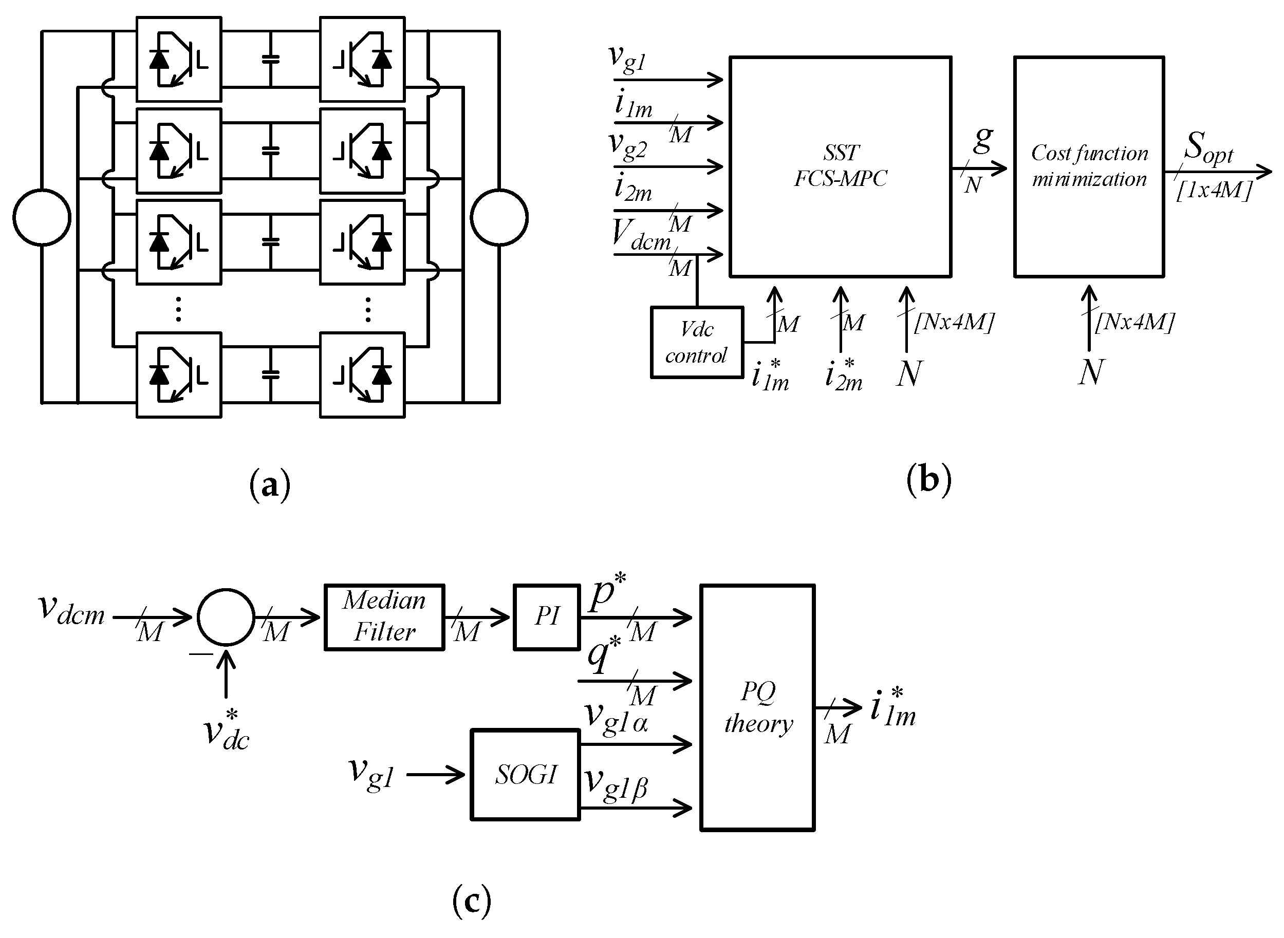
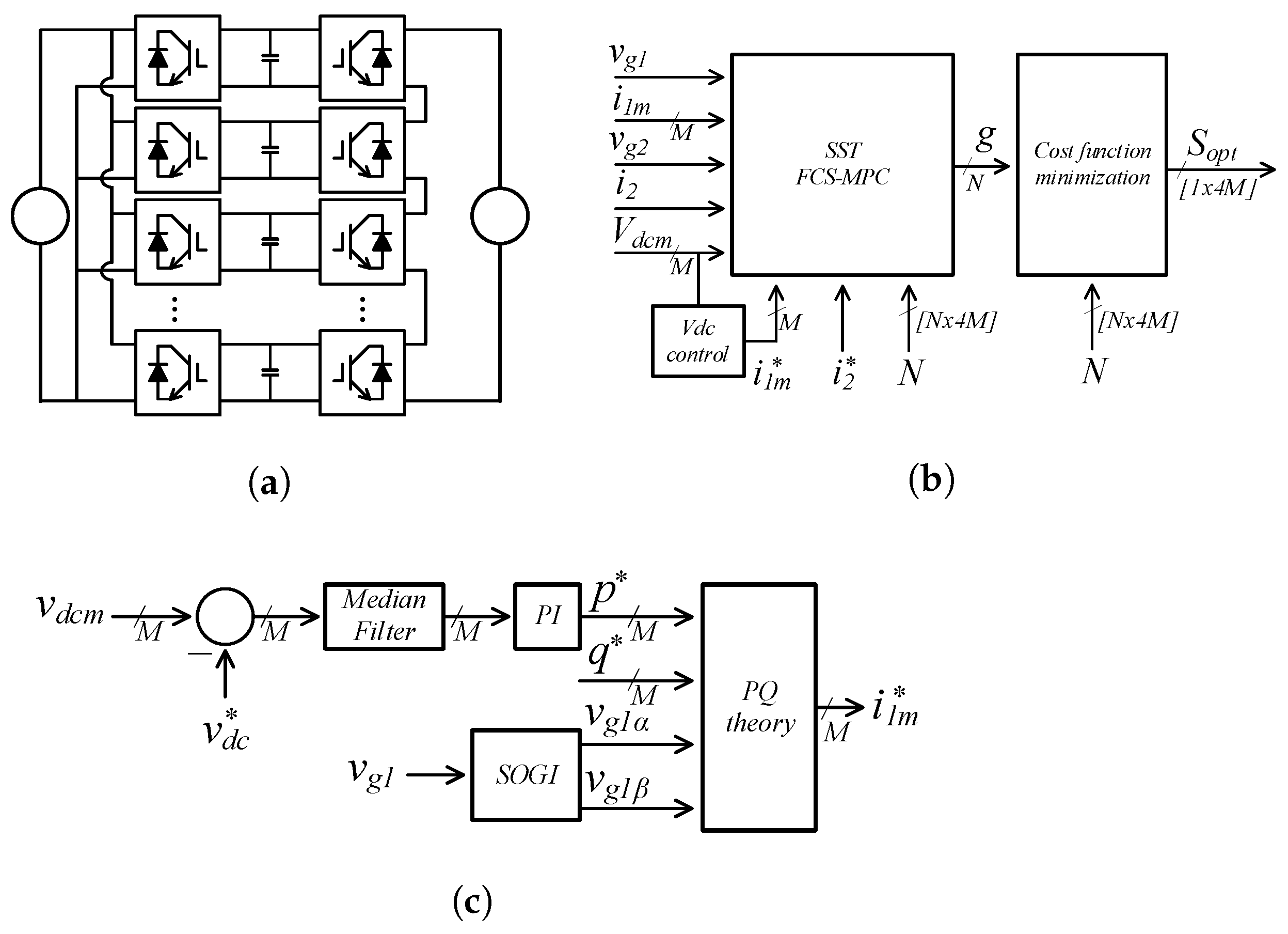
Section 5 details generalized modeling for multiple CHB-B2B converter modules, while Section 6 presents the simulation results in the Simulink/MatLab platform for a 4-modules CHB-B2B in four different arrays. 
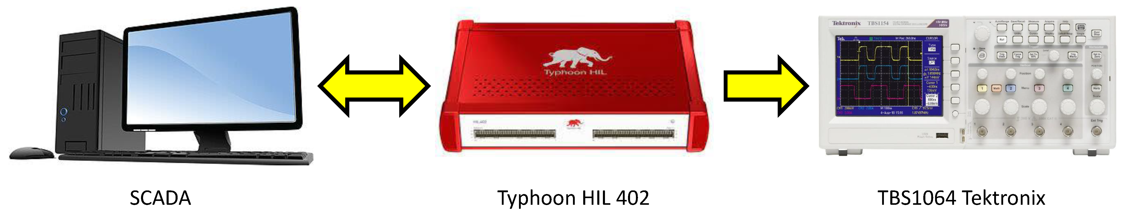
Section 7 presents the real-time experimental results of the Typhoon HIL platform for a 2-modules CHB-B2B in four different arrays, followed by the conclusions in Section 8.

2. Cascaded Multilevel Converters with a Back-to-Back Configuration (CHB-B2B)

The use of equipment based on multilevel converters has developed in a consistent and promising way, developing various equipment, such as back-to-back converters for driving motors or static loads connection; solid-state transformers (SST) for connecting a wide variety of energy sources and grid power flow control; unified power quality conditioners (UPQC) to actively improve the power grid quality; static synchronous compensation (STATCOM) for reactive power compensation, stability improvement, harmonic mitigation, power factor control; and others [19,22,23,24,25].
Furthermore, the increase in voltage levels due to the greater demand for electrical energy has increasingly required the use of multilevel converters to enable direct connections to the medium voltage grid without exceeding the semiconductor switches’ constructive limits. However, the converters’ structural complexity increases considerably with the rise in their voltage levels, making their design and especially their control more difficult. Figure 1 graphically illustrates the number of the components by voltage levels ratio evolution of classical multilevel converter topologies, namely diode-clamped multilevel converter (DCMC); capacitor-clamped multilevel converter (CCMC); modular multilevel converter (MMC); and cascaded H-bridge multilevel converter (CHB). As can be seen in Figure 1, the CHB topology can achieve higher voltage levels with fewer components (it is considered a half-bridge configuration for MMC topology). Furthermore, due to its modular structure, the CHB enables straightforwardly the additional of series cells connection if an output voltage increase is required without any need for including clipping circuits [26].
Figure 2 shows a single-phase CHB multilevel converter with three B2B modules, composed of six H-bridge cells, with an input series and output-parallel (ISOP) arrays. Other arrangements are developed in Section 5 to demonstrate the proposed graph theory methodology scalability.
The CHB-B2B structure presents singularities regarding the control strategies used, such as the impossibility to drive this topology through conventional pulse width modulation (PWM) due to the appearance of several internal short circuit states, as highlighted in Figure 2. For example, for the 3-modules CHB-B2B in the ISOP array, the converter has 24 semiconductor switches, totaling 2 12 different switching states (4096), of which 104 switching states are valid and do not generate internal short circuits, representing approximately only 2.5% of the converter total switching states. This limitation corroborates the importance of developing an automatic methodology for mapping all the prohibitive converter states. Thus, the proposed mapping graph theory methodology is addressed in Section 3 to support the MPC strategy used to control the CHB-B2B converter.

3. Graph Theory Methodology for Mapping the Possible Switching States

As mentioned, a CHB-B2B structure applied as a static converter to achieve some control objective may generate internal short circuits according to the switching performed, making it necessary to find out in which switching states this event is observed. This can be done from a circuit visual inspection. However, the bigger it is, the greater the complexity of this task. Moreover, it is not possible to know whether all the prohibitive states have been found, making this strategy inefficient and doubtful. Hence, an efficient alternative solution that arises to this question is the use of graph theory.
A graph is a mathematical structure used to model relationships between objects of a certain set and is defined as G = G ( V , E ) , in which V is a non-empty finite set of elements denominated as vertices, and E is a set of subsets { u , v } , where u,v ϵ V are denominated as edges. A graph can be directed or not, in which for the first case, the edges will consist of ordered pairs called arcs. Thus, an e = { u , v } arc will be directed from u (head) to v (tail). From a graph, it is possible to trace paths, which can be informally defined as a sequence of vertices and edges, without repetition. A path that does not have loops, orientation and multiple edges is defined as simple. A path that starts and ends at the same vertex consists of a cycle. However, a graph that does not fulfill this condition is called acyclic. In the case that in a graph there is at least one path that interconnects any pair of its vertices, it is called a connected graph. If this same graph is acyclic, it will consist of a tree [27].
In the graph theory universe, some algorithms can be used to trace specific paths. Among them, breadth-first search (BFS) appears as an option to find all possible simple paths from one vertex to another. This algorithm is used for either directed or undirected graphs, and briefly, its working principle consists of the following: starting from an origin vertex u, the BFS algorithm explores systematically the edges of a graph to find all other vertices that are reachable from vertex u and computes the distance between them. The algorithm produces a u-origin tree that contains all reachable vertices. For each vertex v attainable from the origin vertex u, the simple path that connects these two vertices in the obtained tree will also consist of the shortest path that connects these elements in the analyzed graph [28].
Considering electrical nodes as vertices, and electrical switches as edges, a CHB-B2B electrical circuit can be modeled as a connected and undirected G graph [29] (Figure 3) for a namely 3-modules CHB-B2B in ISOP array (Figure 2), where the vertices of the resulting graph are highlighted ( P 1 , P 2 , P 3 , N 1 , N 2 , N 3 , E 1 , E 2 , S 1 , S 2 ). The list of edges of the formed graph and a correlation of these with the static switches are presented in Table 1. As can be observed, three paths are tracked in Figure 3. The red one corresponds to the short circuit highlighted in red in Figure 2. The others, in blue, correspond to distinguish paths that form the short circuit highlighted in blue in Figure 2.
To find all the converter prohibitive switching states, initially, the conditions that can lead to a short circuit must be defined, which are as follows: the terminals of each capacitor become shorted (as highlighted in red in Figure 2), and the opposite terminals of a group of capacitors become connected (as highlighted in blue in Figure 2), which implies a ring with series connections of these capacitors. This results for the topology are used as an example, in the interconnections between capacitors, as it is shown in Figure 4. Thus, by finding simple paths in a graph that interconnect vertices which represent both terminals of a capacitor ([ P 1 , N 1 ], [ P 2 , N 2 ], [ P 3 , N 3 ]), it is possible to visualize part of the prohibitive switching states, which results in circuits like the ones highlighted in Figure 4a–c. The other part of the prohibitive switching states is obtained by joining disjoint paths (paths that do not share any vertex) that interconnect different pairs of opposite terminals for any number of capacitors ([ P 1 , N 2 ], [ P 1 , N 3 ], [ P 2 , N 1 ], [ P 2 , N 3 ], [ P 3 , N 1 ], [ P 3 , N 2 ]). These paths must be disjointed because an electric current flows “from one vertex to another”, without repetition. Thus, vertex sequences [ P 1 , N 2 , P 2 , N 1 ], [ P 1 , N 3 , P 3 , N 1 ], [ P 2 , N 3 , P 3 , N 2 ], [ P 1 , N 3 , P 3 , N 2 , P 2 , N 1 ] and [ P 1 , N 2 , P 2 , N 3 , P 3 , N 1 ] can be formed, which will have the same meaning of circuits as the ones highlighted in Figure 4d–h, respectively.
All these paths can be found using a modified BFS algorithm. However, the algorithm should be able to ignore paths that represent obvious short circuits, such as those that occur when two switches of the same H-bridge’s leg are turned on. This condition itself is ignored by the converter control law, which should interlock these switches, limiting the sample space of the switching possibilities, reducing it to 2 L states, where L is the number of legs in the converter topology.
The biggest challenge that emerges from this task is to check all possible combinations that form the mentioned ring with a series capacitor connection, which increases exponentially, as there is an increment in the number of the capacitors. A short circuit could occur with two, or as many capacitors the topology has, and their position into the series connection could be permuted, with each representing a different converter switching state. To solve this issue, a possible solution is to apply an abstraction that models a new directed graph named H, in which vertices consist of a representation of terminals’ pairs from different polarities and capacitors ( P 1 N 2 , P 1 N 3 , P 2 N 1 , P 2 N 3 , P 3 N 1 , P 3 N 2 ). Notably, each of these H vertices correspond to a set of traced paths that interconnect the G graph vertices. Meanwhile, the edges will interconnect vertices whose negative terminal on the first corresponds to the same capacitor as the positive terminal of the second vertex (e.g., [ P 1 N 2 , P 2 N 3 ]), as shown in Table 2 for 3-modules CHB-B2B in the ISOP array. Figure 5 presents the resulting H graph.
Finally, all possible combinations of interconnection between the capacitors are obtained using BFS from the tracing of some possible paths that respect certain laws. Each path must have a source u and a target vertex v in which the positive terminal index of the representation of a vertex u coincides with the negative terminal index of the representation of a vertex v (e.g., [ P 1 N 3 , P 2 N 1 ]), as shown in Table 3 for the 3-modules CHB-B2B in ISOP array. However, not all possible paths found generate only one short circuit possibility for series-connected capacitors. Indeed, there are some restrictions, such as paths being unable to have vertices with the same positive terminal index in the corresponding interconnection (e.g., P 1 N 2 and P 1 N 3 ). Moreover, paths cannot have vertices that have the same negative terminal index (e.g., P 1 N 2 and P 3 N 2 ) in the corresponding interconnection. These restrictions are necessary, as they represent interconnections between capacitors with multiple short circuits and would only consist of unnecessary redundancies. Two cases in which this situation occurs in the H graph are highlighted (in red) in Figure 6, where the connection between the vertices P 1 N 2 with P 2 N 1 is performed.
Figure 7 elements show the possible paths (in blue) that can be traced with the BFS algorithm for the 3-modules CHB-B2B in the ISOP array. It can be highlighted that Figure 7a,e represent the same capacitors interconnection, and the same thing occurs for other Figure 7 elements, such as Figure 7b,g,j; Figure 7c,f,k; Figure 7d,i; and finally, Figure 7h,l. Relating all the paths shown in Figure 7 with Figure 4 elements, it can be observed that the elements Figure 7a–d,h represent the connection conditions of Figure 4d–h, respectively.
As discussed, with the results obtained from paths traced in the H graph, each vertex of these paths corresponds to a set of paths traced in the G graph, which can be combined to obtain a physical path of the electric current that represents a state of the short circuit in the converter. For each finally obtained path, the union of consecutive vertices to be visited corresponds to an edge, which has the physical meaning of a static switch with an O N state. The edges that are not part of the analyzed path have an indeterminate state, being able to assume O N and O F F values. Thus, a converter’s prohibitive switching matrix containing all the prohibitive switching states of the converter can be formed and used to obtain the valid converter switching matrix from a matrix containing all possible switches.
Figure 8 presents a flowchart overview of the proposed strategy to obtain the desired converter switching matrix.

4. Model Predictive Control (MPC)

Model predictive control, initially introduced in the process industry in the 1970s, addresses a broad concept, consisting of predicting all system future states in a given time horizon, based on a mathematical model [30,31,32,33,34]. An optimized control action is then chosen to minimize a function that is based on a reference and predicted states, also known as a cost function. The use of MPC in power electronics began in the 1980s in low switching frequency applications since higher switching frequencies require more complex calculations due to the fact that cost function optimization requires a lot of computational effort, which was not available at that time [30,31,35,36]. It was only from the 1990s onwards that this technology had a leap of development due to the great technological advance of microprocessors capable of performing a large number of mathematical operations. Thus, the interest in using the MPC in applications with previously unfeasible high switching frequency has intensified, gaining the attention of power electronics researchers. Furthermore, the MPC is a simple and intuitive way to control the converters, being capable of dealing with multivariable goals, with good controllability, fast dynamic response, and the capacity to incorporate, in a straightforward way, nonlinearities and constraints into the control law [37]. MPC is divided into two classes regarding the optimization problem nature, as shown in Figure 9.
Due to the discrete characteristics of power electronics applications, the finite control set MPC (FCS-MPC) makes their implementation simpler since it does not require modulation techniques to act on the converter [30,37,38]. The optimal switching vector MPC (OSV-MPC) was the first predictive control strategy adopted in power electronics applications and is still the most widely used today due to its low implementation complexity and rapid dynamic response. However, as a disadvantage, this class presents a variable switching frequency. Nevertheless, some studies aim to minimize the frequency harmonic spectrum dispersion by incorporating specific goals into the cost function [38,39].
Power electronics-based systems have as their main characteristic the finite number of switching states, so in power electronics converters, the control action is limited to the set of switching states possible in the converter, making the MPC an option that is feasible and easy to implement. Its cost function is directly associated with the controlled variables set.
At each sampling time, the microprocessors perform various calculations and predict the variables future for each possible switching state based on the predictive model, measurements and system states. Then, the switching state with the lowest cost is applied to the converter. Thus, this control technique is intrinsically linked to the switching process, dispensing the use of a modulation technique.
Although the MPC is an open-loop optimization algorithm, when repeated at each sampling time, it behaves like a feedback loop control based on optimization, making its dynamic response quick in the face of reference variations or disturbances [30].

5. CHB-B2B Converter Modeling

The presented strategy based on graph theory to obtain the switching matrix of any CHB-B2B converter is evaluated via computational simulations (Section 6) and physical implementation through an HIL platform (Section 7). Thus, different CHB-B2B configurations are proposed, and the MPC principles are applied as a control strategy. Therefore, it is necessary to determine the whole system, the filters designs, the control goals, and the mathematical models for predicting the control variables for the different proposed topologies. All these steps are presented in this section.

5.1. Generalized M-Modules CHB-B2B Converter

Figure 10 presents a generalized representation of the M-modules CHB-B2B converter, in which the input array and output array blocks (hatched areas) consist of series or parallel connections between the different converters’ H-bridge cells. The index m represents which converter module that a given variable is referring to. On the other hand, the variable n is related to the side of the converter. Thereby, for the module’s currents in each module highlighted above, i 1 m is considered the current on the primary side ( n = 1 ) of the m’th module, and i 2 m as the current on the secondary side ( n = 2 ) of the m’th module. In a similar way, V d c m represents the DC-link voltage of the m’th module, v 1 m is the switched voltage on the primary side ( n = 1 ) of the m’th module, and v 2 m is the switched voltage on the secondary side ( n = 2 ) of the m’th module. Either the primary or secondary converter sides are connected to electrical grids, with the power flow from the first one ( v g 1 ) to the second ( v g 2 ). Thus, the main objective control is to synthesize an appropriate power quality output current i 2 , necessitating a voltage balance in the DC-links through their capacitances. Consequently, the converter’s power flow control must be achieved by controlling the primary input current i 1 . Both current controls can be obtained by applying an inductive filter with a small resistance representing electrical losses. However, the design of these elements may be hampered due to the variable switching frequency inherent in the OSV-MPC strategy.
As it can be noted, for the converter’s primary side, if the input array consists of a series connection between the H-bridge cells, the input current i 1 is equal to each module’s primary current ( i 1 m ). The same thing occurs for the converter’s secondary side, in which, for a series connection output array, the output current i 2 is the same as the module’s secondary current ( i 2 m ). However, inversely, the switched voltages v 1 and v 2 consist in the summation of each module’s switched voltages that composes each side of the converter (e.g., v 1 = 1 M v 1 m and v 2 = 1 M v 2 m ). For a different condition, with an input and output array consisting of parallel connection, input and output current ( i 1 and i 2 , respectively) now consist in the summation of each module’s currents (e.g., i 1 = 1 M i 1 m and i 2 = 1 M i 2 m ).

5.2. Primary/Secondary Inductive Filters and DC-Link Capacitances

The design of the currents’ filters can be obtained by the following methodology. Defining the nominal rating of the DC-link voltage as V d c , the maximum allowed variation of the filter current in each module as Δ i n m and f s as the switching frequency of the converter, the required filter inductance for any module of the n side of the converter (primary and secondary) can be calculated with Equation (1). The value of Δ i n which defines Δ i n m (according to connection type and number of modules) can be determined from a defined percentage of the nominal filter current peak value i n , p k ; in this research paper, a value of 5% is considered. For the OSV-MPC control strategy, as the switching frequency is variable due to the dispersed harmonic spectrum, f s is considered as the control’s operation frequency, which corresponds to the inverse of the sampling period T s .
l n = V d c 2 Δ i n m f s
The procedure to calculate the value of i n , p k is presented in (2), in which P T corresponds to the power demanded by the converter, and V g n is the grid nominal effective value.
i n , p k = 2 i n = 2 P T V g n
For modeling the parasitic resistance present in each filter ( r n ), its value is adopted as a percentage of the reactance relative to the filter’s inductance, as described by Equation (3), where f g corresponds to the primary grid frequency.
r n = X l n 100 = 2 π f g 100
The DC-link capacitance design for the m’th module ( C d c m ) can be obtained from Equation (4) by setting the desired voltage ripple variation Δ V d c and from the already defined variable P T [20], where ω is the angular velocity defined as 2 π f g , and M is the number of modules connected in a back-to-back configuration in the converter. The value of Δ V d c can be determined from a defined percentage of the nominal DC-link voltage V d c . In this research paper, a value of 1% is considered for Δ V d c .
C d c m = 1 M P T ω V d c Δ V d c
After defining the filters’ structures and the elements of the system, the mathematical models of the controlled electrical variables for MPC application can be obtained and are described in the next sections for different CHB-B2B converter configurations. Furthermore, a cost function is defined to fulfill the OSV-MPC strategy and its minimization defines the optimal switching sequence. For its construction, the reference variables must be defined according to the control objectives.

5.3. Mathematical Models and Cost Function for Different Topologies

The OSV-MPC strategy implementation requires the dynamic equations for the converter’s primary and secondary currents, and for the DC-links voltage that must be regulated for a nominal value. Considering S m j representing the j’th S switch in the m’th converter’s module (e.g., Figure 2), it can be determined Equations (5) and (6) that express the state of each primary or secondary H-bridge cells of the m’th module, defined as d 1 n and d 2 n , respectively. Consequently, according to the switches’ states, d 1 n and d 2 n can assume the values set of (−1, 0, 1).
d 1 m = S m 1 S m 4 S m 2 S m 3
d 2 m = S m 5 S m 8 S m 6 S m 7
Therefore, the following relationships can be defined, according to the realized connection’s type. For series connections, Equations (7) must be used, while for parallel connections, Equation (8) is valid.
v n = m = 1 M d n m V d c m
i n = m = 1 M d n m i n m

5.3.1. Generic M-Modules ISOS (Input-Series Output-Series)

An example of an ISOS CHB-B2B configuration is highlighted in Figure 11a. The dynamic equation for the m’th module DC-link voltage level ( V d c m ) can be obtained considering the input ( i 1 ) and output ( i 2 ) filters’ currents and is presented in Equation (9). As can be observed, if d 1 m has a positive and d 2 m a negative value, the DC-link is going to be charged, whereas, for opposite values for these terms, DC-link must be discharged.
d V d c m d t = 1 C d c m ( d 1 m i 1 m d 2 m i 2 m )
As the control loop is composed of the grid connections and inductive filters, the dynamic models of the described i 1 and i 2 currents can be represented by Equations (10) and (11), in which v 1 and v 2 values are obtained from Equation (7).
d i 1 d t = 1 M l 1 ( v g 1 M r 1 i 1 v 1 )
d i 2 d t = 1 M l 2 ( v 2 M r 2 i 2 v g 2 )
Figure 11b presents a diagram block that exemplifies the implementation of the OSV-MPC, necessary to achieve the control objectives, namely synthesizing the appropriate i 1 and i 2 currents, keeping the DC-links regulated. The system’s electrical magnitudes ( v g n , i n , V d c m ) are measured and, by modeling the system, these variables are predicted for a future instant. Based on the dynamic equations above, Equations (9)–(11), the discrete equations necessary for the OSV-MPC application are obtained using the Euler numerical integration method and defining [k] and [ k + 1 ], as the present and future instants, respectively. They are presented in Equations (12)–(14) below, considering the T s sampling period. From these predictions and the determination of references for the control variables, a cost function is defined, whose minimization provides which switching is the most optimal in the future instant for the control objectives.
V d c m [ k + 1 ] = V d c m [ k ] + T s C d c m d 1 m [ k ] i 1 m [ k ] T s C d c m d 2 m [ k ] i 2 m [ k ]
i 1 [ k + 1 ] = 1 r 1 m l 1 m i 1 [ k ] + T s M l 1 m v g 1 T s M l 1 m v 1 [ k ]
i 2 [ k + 1 ] = 1 r 2 m l 2 m i 2 [ k ] T s M l 2 m v g 2 + T s M l 2 m v 2 [ k ]
To obtain the OSV-MPC cost function, the next step is to define the reference signals for the V d c m , i 1 and i 2 control variables, which is represented with an asterisk suffix, as presented in Figure 11b. For V d c m * , DC-link voltage nominal operating rating is used. Applying Equation (2), i 2 * can be generated from a sinusoidal signal with f g frequency and nominal i 2 peak value ( i 2 , p k ). The primary reference current i 1 * is dynamically calculated and is in phase with the v g 1 grid voltage from PQ theory [40], together with a second order generalized integrator (SOGI) [41], as presented in Figure 11c. This current enables the power flow control to be achieved ensuring DC-links capacitance–voltage maintenance and system balance. Therefore, the cost function g N can be defined by Equation (15), with V d c ¯ consisting of the average of the DC-link voltages, where N is the valid switching states defined by the graph theory which do not result in an internal short circuit. Weights are defined to designate which control object should be prioritized: i 1 * current synthesis ( W 1 ), i 2 * current synthesis ( W 2 ), regulation of DC-links ( W d c ), or balance of DC-links ( W b l ). In this research paper, all weights are defined with unit values ( W 1 = W 2 = W d c = W b l = 1.0 ). Thus, all the cost function objectives have the same importance.
g I S O S N = W d c M m = 1 M ( V d c * V d c m ) 2 + W b l M m = 1 M ( V d c ¯ V d c m ) 2 + W 1 ( i 1 * i 1 ) 2 + W 2 ( i 2 * i 2 ) 2
Multiple values of the cost function are obtained, totaling N values, for different switching states of the converter. The cost function minimization, that is, the switching state that produces the lowest value corresponds to an optimal switching ( S o p t ) that should be used at the time step [ k + 1 ] .

5.3.2. Generic M-Modules IPOP (Input-Parallel Output-Parallel)

An example of an IPOP CHB-B2B configuration is highlighted in Figure 12a. The generic dynamic Equation (9) for the m’th module DC-link voltage level ( V d c m ) can be obtained considering the m’th module input ( i 1 m ) and output ( i 2 m ) currents, since in this case, they differ from the input ( i 1 ) and output ( i 2 ) currents of the converter, respectively. The same previous capacitor charge and discharge analysis will remain valid for this situation.
Differently for the ISOS converter case, the input ( i 1 ) and output ( i 2 ) currents are indirectly controlled by the individual control of each module’s currents. Therefore, dynamic models of i 1 m and i 2 m currents are necessary and can be represented by Equations (16) and (17).
d i 1 m d t = 1 M l 1 ( v g 1 r 1 i 1 m v 1 m )
d i 2 m d t = 1 M l 2 ( v 2 m r 2 i 2 m v g 2 )
Figure 12b presents a diagram block that exemplifies the implementation of the OSV-MPC for IPOP configuration. The system’s electrical magnitudes ( v g n , i n m , V d c m ) are measured, and these variables are predicted for a future instant by the modeled system. Again, the discrete equations necessary for the OSV-MPC application are obtained using the Euler numerical integration method, using (9), (16), and (17), and they are expressed by Equations (12), (18), and (19).
i 1 m [ k + 1 ] = 1 r 1 l 1 i 1 m [ k ] + T s l 1 v g 1 T s l 1 v 1 m [ k ]
i 2 m [ k + 1 ] = 1 r 2 l 2 i 2 m [ k ] T s l 2 v g 2 + T s l 2 v 2 m [ k ]
For the cost function definition, the V d c m * reference is newly considered as the DC-link voltage nominal operating rating value. The secondary currents of m’th module ( i 2 m * ) reference values are obtained by applying Equation (2) and generating a sinusoidal signal with f g frequency and an amplitude corresponding to the m’th part of the nominal i 2 peak value ( i 2 , p k / M ). Similarly, to the ISOS case, i 1 m * references are obtained, as seen in Figure 12c, by PQ theory application together with a second order generalized integrator (SOGI). Therefore, the cost function g N can be defined by Equation (20).
g I P O P N = W d c M m = 1 M ( V d c * V d c m ) 2 + W b l M m = 1 M ( V d c ¯ V d c m ) 2 + W 1 M m = 1 M ( i 1 m * i 1 m ) 2 + W 2 M m = 1 M ( i 2 m * i 2 m ) 2

5.3.3. Generic M-Modules ISOP (Input-Series Output-Parallel)

ISOP CHB-B2B configuration consists of recombining the ISOS and ISOP configurations which are already presented (Figure 13a). Figure 13b presents a diagram block that exemplifies the implementation of the OSV-MPC for ISOP configuration. The system’s electrical magnitudes ( v g n , i 1 , i 2 m , V d c m ) are measured, and these variables are predicted for a future instant by the modeled system.
The primary side of this topology has the same dynamics as the ISOS configuration and, therefore Equations (10) and (13) here are also valid. The secondary side, in turn, has the same dynamics as the IPOP configuration and, therefore, Equations (17) and (19) must be considered. Finally, as previously discussed, the dynamic for m’th module DC-link voltage level ( V d c m ) is described by Equation (9), and its discretization results in (12).
The reference signal V d c m * still consists of the nominal value of V d c . The same i 1 * reference applied in the ISOS, as presented in Figure 13c, and i 2 m * reference applied in the IPOP configurations is used to define the ISOP converter cost function, which is presented in (21).
g I S O P N = W d c M m = 1 M ( V d c * V d c m ) 2 + W b l M m = 1 M ( V d c ¯ V d c m ) 2 + W 1 ( i 1 * i 1 ) 2 + W 2 M m = 1 M ( i 2 m * i 2 m ) 2

5.3.4. Generic M-Modules IPOS (Input-Parallel Output-Series)

An example of an IPOS CHB-B2B configuration is highlighted in Figure 14a. This configuration consists of recombination between the IPOP and ISOS configurations, which are already presented. Figure 14b presents a diagram block that exemplifies the implementation of the OSV-MPC for IPOS configuration. The system’s electrical magnitudes ( v g n , i 1 m , i 2 , V d c m ) are measured, and these variables are predicted for a future instant by the modeled system.
The primary side of this topology has the same dynamics as the IPOP configuration and therefore, Equations (16) and (18) here are also valid. The secondary side, in turn, has the same dynamics as the ISOS configuration and, therefore, Equations (11) and (14) must be considered. Finally, as previously discussed, the dynamic for m’th module DC-link voltage level ( V d c m ) is described by Equation (9), and its discretization results by (12).
The reference signal V d c m * still consists of the nominal value of V d c . The same i 1 m * reference applied in the IPOP, as presented in Figure 14c, and i 2 * reference applied in the ISOS configurations is used to define the IPOS converter cost function, which is presented in Equation (22).
g I P O S N = W d c M m = 1 M ( V d c * V d c m ) 2 + W b l M m = 1 M ( V d c ¯ V d c m ) 2 + W 1 M m = 1 M ( i 1 m * i 1 m ) 2 + W 2 ( i 2 * i 2 ) 2

5.4. Graph Theory Results

From the proposed strategy based on graph theory to find the switching matrix for static converters, different results can be obtained and are presented in Table 4, which shows a review of the characteristics for different CHB-B2B topologies. Indeed, as the number of converter modules increases, the use of its switching states (U [%]) decreases, due to the increment in the possibilities of short circuits, although, at the same time, the number of valid switching states (N) increases. It is also noticed that, for the same number of modules, serial configurations present a smaller number of short circuits when compared to parallel ones. However, the main point to be highlighted is the number of levels that can be synthesized for each side of the converter. In fact, a parallel connection always synthesizes three voltage levels, but this does not occur for serial connections, where the number of modules increases, the number of possible levels to be synthesized by the converter tends to increase. For ISOS connections, all these voltage levels are achievable, therefore allowing the converter associated with a filter to have a better harmonic spectrum. However, due to the occurrence of short circuits, this does not occur for the ISOP and the IPOS configurations, in which the series side is limited to only five levels, regardless of the number of modules used.
With the increase in the number of converter modules, the switching matrix increases in an exponentially way, that is, the sample space to be analyzed by the OSV-MPC algorithm may become unfeasible for digital implementations, despite the mentioned advance in microcontrollers. As an example, shown in Table 4, the 6-module ISOS configuration control must, at each time step, perform 124,416 calculations to predict which, among 124,416 switching states, is considered optimal for the future instant. Therefore, in a first analysis, without applying some type of optimization in the control strategy, the physical implementation of this converter is unfeasible. Hence, the results presented in Table 4 demonstrate the importance of applying graph theory to the objectives proposed in this article, in which it is possible to detail the characteristics of the different configurations of CHB-B2B converters and their switching matrices, to contribute to defining the most advantageous topology and its applicability.

6. Simulation Results for 4-Modules CHB-B2B

After defining the discrete equations for each topology of the CHB-B2B, the values of the converter’s elements must be projected to perform OSV-MPC. Initially, based on a 4-modules ISOS CHB-B2B topology, electrical grids having 1440 V peak voltage are considered. Therefore, the nominal value for the DC-links can be obtained from the division of the grid voltage and the number of converter modules ( V n ^ = 360 V), considering a modulation factor m a , according to Equation (23). In this research paper, a 4/5 is considered since a minimum 3/4 modulation factor is necessary to obtain the nine voltage levels of this topology [42].
V d c = V n ^ m a = v g , p k M m a
Thus, a 450 V is achieved for the DC-links voltage value, and it is used for all other CHB-B2B configurations (IPOP, ISOP, and IPOS). However, due to the limitations of these configurations caused by the smallest number of possible switches, a modulation factor of 2/3 is considered, in order to obtain a “slack” for the converter, resulting in a value of V n ^ equal to 300 V.
The next step is to define other parameters, such as the switching frequency f s , the power demanded by the converter P T and the grid frequency f g , for which 20 kHz , 10 kVA and 50 Hz values are respectively considered. Different switching and grid frequency values for each side of the converter could be considered.
For parallel connection sides, the value of V n ^ should be considered as the peak voltage of the connected grid since the converter is limited to three voltage levels as discussed ( V n ^ = v g , p k ). For mixed series/parallel configurations (ISOP, IPOS), due to the serial connection being limited to five levels, a value of 2 V n ^ is considered as the peak voltage of the connected grid (2 V n ^ = v g , p k ). Finally, using Equations (1)–(4), Table 5 can be constructed, which shows the values of the converter elements for different configurations of a 4-modules CHB-B2B example.

6.1. 4-Modules CHB-B2B Simulation Results

From the dimensioning performed and presented in Table 5 for different configurations of 4-modules CHB-B2B converters, the graph theory application as a solution to obtain the switching matrix of these converters can be validated. The steady-state performance of the OSV-MPC control systems presented in this section is verified via simulation, through the Simulink/Matlab computational platform, to confirm the non-occurrence of internal short circuits in the converter and that the control objectives are reached.

6.1.1. 4-Modules ISOS Configuration

The results of the 4-modules ISOS CHB-B2B topology are presented below, in which the steady-state behavior of the currents on the primary ( i 1 ) and secondary sides ( i 2 ), DC link voltages ( V d c m ) and the switching voltages on the primary ( v 1 ), secondary ( v 2 ) of each converter module ( v n m ) are highlighted. As can be seen in Figure 15a,b, the converter can synthesize the expected nine voltage levels, both on the primary and secondary sides. It is also verified that each module presents a variable switching frequency, without a defined pattern.
Figure 15c shows that the DC-links could be tuned to nominal values, as compared to the V d c * reference, which is essential for the correct control operation. However, as CHB does not have natural three-phase characteristics, the DC-links voltages present an oscillation with the double of the fundamental grid frequency (50 Hz) [20]. In Figure 15c, a maximum 2 V (0.44%) oscillation in the magnitude is observed, which conforms to the DC-link design requirements (4.5 V).
The currents in the primary and secondary of the converter are verified in Figure 15d,e, respectively. As can be seen, they satisfactorily follow the i 1 * and i 2 * references and are in phase with the v g 1 and v g 2 grid voltages, making the converter power factor unitary. A maximum 0.2 A (1.44%) oscillation in i 1 is obtained, while for i 2 , a 0.14 A (1%) value is observed, which conforms to the filter design requirements (0.69 A). Finally, it can be concluded that the control system operates properly, making it possible to affirm that the used converter switching matrix eliminates all the prohibitive switching states.

6.1.2. 4-Modules IPOP Configuration

The results of the 4-modules IPOP CHB-B2B topology are presented below, in which the steady-state behavior of the currents on the primary ( i 1 ) and secondary sides ( i 2 ), modules’ currents ( i n m ), DC link voltages ( V d c m ) and switching voltages of each converter module ( v n m ) are highlighted. As can be seen in Figure 16a,b, the converter can synthesize only three voltage levels, both on the primary and on the secondary sides, as it is expected. It is also verified that each module presents a variable switching frequency, without a defined pattern.
Figure 16c shows that the DC-links could be tuned to nominal values. Compared to the V d c * reference, a maximum 2.5 V (0.55%) oscillation in the magnitude is obtained, which conforms to the DC-link design requirements (4.5 V). The currents in the primary and secondary of the converter are verified in Figure 16d,e, respectively. As it can be seen, they satisfactorily follow the i 1 * and i 2 * references and are in phase with the v g 1 and v g 2 grid voltages, making the converter power factor unitary. Each primary module’s currents which constitute i 1 are the same and they are superimposed on the graph. The same thing happens for the currents that constitute i 2 .
A maximum of 2.15 A (3.25%) oscillations in i 1 and i 2 current components are observed, which conforms to the filter design requirements (3.33 A). Finally, the control system operates properly, which affirms that the used converter switching matrix eliminates all the prohibitive switching states.

6.1.3. 4-Modules ISOP Configuration

The results of the 4-modules ISOP CHB-B2B topology are presented below, in which the steady-state behavior of the currents on the primary ( i 1 ) and secondary sides ( i 2 ), secondary modules’ currents ( i 2 m ), DC link voltages ( V d c m ) and switching voltages on the primary ( v 1 ) and of each converter module ( v n m ) are highlighted. As can be seen in Figure 17a,b, the converter can synthesize only five voltage levels as expected, on the primary side. On the secondary side, due to the parallel connection, only five voltage levels are synthesized. It is also verified that each module presents a variable switching frequency, without a defined pattern.
Figure 17c shows that the DC-links could be tuned to nominal values, as compared to the V d c * reference, with a maximum 3.5 V (0.77%) oscillation in the magnitude, which conforms to the DC-link design requirements (4.5 V). The currents in the primary and secondary of the converter are verified in Figure 17d,e, respectively. As it can be seen, they satisfactorily follow the i 1 * and i 2 * references and are in phase with the v g 1 and v g 2 grid voltages, making the converter power factor unitary. Each secondary modules’ currents which constitute i 2 are the same, and they are superimposed on the graph.
A maximum of 0.27 A (0.81%) oscillation in i 1 is obtained, while for i 2 current components a 1.08 A (1.62%) is observed. This conforms to both filter design requirements ( Δ i 1 = 1.67 A and Δ i 2 = 3.33 A). Finally, it can be concluded that the control system works properly, making it possible to affirm that the used converter switching matrix eliminates all the prohibitive switching states.

6.1.4. 4-Modules IPOS Configuration

The results of 4-modules IPOS CHB-B2B topology are presented below, in which the steady-state behavior of the currents on the primary ( i 1 ) and secondary sides ( i 2 ), primary modules’ currents ( i 1 m ), DC link voltages ( V d c m ) and switching voltages on the secondary ( v 2 ) and of each converter module ( v n m ) are highlighted. As can be seen in Figure 18a,b, the converter can synthesize only five voltage levels as it is expected, on the secondary side. On the primary side, due to the parallel connection, only three voltage levels are synthesized. It is also verified that each module presents a variable switching frequency, without a defined pattern.
Figure 18c shows that the DC-links could be tuned to nominal values. When compared to the V d c * reference, a maximum 3.88 V (0.86%) oscillation in the magnitude is obtained, which conforms to the DC-link design requirements (4.5 V). The currents in the primary and secondary of the converter are verified in Figure 18d,e, respectively. As can be seen, they satisfactorily follow the i 1 * and i 2 * references and are in phase with the v g 1 and v g 2 grid voltages, making the converter power factor unitary. Each primary module’s currents which constitute i 1 are the same, and they are superimposed on the graph.
A maximum of 2.12 A (3.18%) oscillation in i 1 current is obtained, while for i 2 , a 0.28 A (0.84%) is observed. This conforms to both filter design requirements ( Δ i 1 = 3.33 A and Δ i 2 = 1.67 A). Finally, it can be concluded that the control system works properly, making it possible to affirm that the used converter switching matrix eliminates all the prohibitive switching states.

6.2. Hybrid Configurations

As discussed, and analyzing Table 5, the ISOP and IPOS configurations for topologies with more than two modules do not allow the synthesis of more than five voltage levels for the side connected in series, due to the switching states that generate short circuits in the converter, making it impossible to take advantage of all the levels. A solution for this, keeping the characteristics of these topologies, is to divide the parallelism into pairs of modules connected in parallel. Thus, all levels on the series side can be synthesized. Therefore, new hybrid topologies could be proposed, namely HISOP (hybrid input-series output-parallel) and HIPOS (hybrid input-parallel output-series), and their characteristics are highlighted in Table 6.

7. Real-Time Experimental Results

All previously presented results were restricted to converter topologies with four modules each in a Simulink/MatLab platform. To obtain more diverse and realistic results, different configurations with two modules were tested using a Typhoon HIL platform in real-time test bench using a software-in-the-loop (SIL) environment. Real results are obtained using an oscilloscope and are presented in this section. The same sizing procedure of the system components performed is necessary. The real-time simulation platform is presented in Figure 19. A Typhoon HIL 402 module is responsible for power and control system real-time simulation. The supervisory control and data acquisition (SCADA) platform provided by HIL402 is used for real-time test-bench configuration and supervision. Finally, a TBS1064 Tektronix oscilloscope is used to acquire the real-time simulation results.

7.1. 2-Modules CHB-B2B Design and Experimental Results

For 2-modules converters, the same 450 V voltage level used previously is considered. Due to the number of modules being reduced by half, the grid voltage levels and the power demanded by the converter P T are reduced in the same proportion for all configurations (ISOS, IPOP, ISOP, and IPOS). The same values of switching frequency f s and grid frequency f g are maintained. Using Equations (1)–(4), Table 7 can be constructed, which shows the converter elements values for different configurations of a 2-modules CHB-B2B example.
Next, the performance in the steady-state of the OSV-MPC control system is verified by employing experimental results, in which the non-occurrence of internal short circuits in the converter can be confirmed. Therefore, the graph theory application as a solution to obtain the switching matrix of these converters is validated. It is also checked whether the control objectives have been achieved.

7.1.1. 2-Modules ISOS Configuration

The results of the 2-modules ISOS CHB-B2B topology are presented in Figure 20, in which the steady-state behavior of the currents on the primary ( i 1 ) and secondary sides ( i 2 ), DC link voltages ( V d c m ) and switching voltages on the primary ( v 1 ), secondary ( v 2 ) and of each converter module ( v n m ) are highlighted. As can be seen in Figure 20a,b, the converter can synthesize the expected five voltage levels, both on the primary and the secondary sides. It is also verified that each module presents a variable switching frequency, without a defined pattern.
Figure 20c shows that the DC-links (orange and blue) could be tuned to nominal values. When compared to the V d c * reference (450 V), a maximum of 0.378 2 = 0.534 V (0.12%) oscillation in the magnitude is obtained, which conforms to the DC-link design requirements (4.5 V). The currents in the primary and secondary of the converter are verified (in blue) in Figure 20d,e, respectively. As can be seen, they have an adequate RMS value corresponding to their nominal values, with a small error in the DC-links measurements, due to the oscilloscope’s impression. Additionally, they are in phase with the v g 1 and v g 2 grid voltages (in orange), making the converter power factor unitary.
A maximum of 0.56 A (3.36%) oscillation in i 1 is obtained, while for i 2 , 0.55 A (3.27%) is observed, which conforms to the filter design requirements (0.83 A). Finally, it can be concluded that the control system works properly, making it possible to affirm that the used converter switching matrix eliminates all the prohibitive switching states.

7.1.2. 2-Modules IPOP Configuration

The results of the 2-modules IPOP CHB-B2B topology are presented in Figure 21, in which the steady-state behavior of the currents on the primary ( i 1 ) and secondary sides ( i 2 ), modules’ currents ( i n m ), DC link voltages ( V d c m ) and switching voltages of each converter module ( v n m ) are highlighted. As can be seen in Figure 21a,b, the converter can synthesize only three voltage levels, both on the primary and the secondary sides, as expected. It is also verified that each module presents a variable switching frequency, without a defined pattern.
Figure 21c shows that the DC-links (orange and blue) could be tuned to nominal values. When compared to the V d c * reference (450 V), a maximum 0.782 2 = 1.11 V (0.25%) oscillation in the magnitude is obtained which conforms to the DC-link design requirements (4.5 V). The currents in the primary and secondary of the converter are verified (in blue) in Figure 21d,e, respectively. As can be seen, they have an adequate RMS value corresponding to their nominal values, with a small error in the DC-links measurements, due to the oscilloscope’s impression. Additionally, they are in phase with the v g 1 and v g 2 grid voltages (in orange), making the converter power factor unitary. Each primary module’s currents which constitute i 1 are the same and they are superimposed on the graph (violet and green signals). The same thing happens for the currents that constitute i 2 .
A maximum 1.12 A (3.36%) oscillation in i 1 is obtained, while for i 2 , 1.09 A (3.26%) is observed, which conforms to the filter design requirements (1.67 A). Finally, it is concluded that the control system works properly, making it possible to affirm that the used converter switching matrix eliminated all the prohibitive switching states.

7.1.3. 2-Modules ISOP Configuration

The results of the 2-modules ISOP CHB-B2B topology are presented in Figure 22, in which the steady-state behavior of the currents on the primary ( i 1 ) and secondary sides ( i 2 ), secondary modules’ currents ( i 2 m ), DC link voltages ( V d c m ) and switching voltages on the primary ( v 1 ) and of each converter module ( v n m ) are highlighted. As can be seen in Figure 22a,b, the converter can synthesize only five voltage levels as it is expected, on the primary side. On the secondary side, due to the parallel connection, only three voltage levels are synthesized. It is also verified that each module presents a variable switching frequency, without a defined pattern.
Figure 22c shows that the DC-links (orange and blue) could be tuned to nominal values, since when compared to the V d c * reference (450 V), a maximum 0.574 2 = 0.812 V (0.18%) oscillation in the magnitude is obtained, which conforms to the DC-link design requirements (4.5 V). The currents in the primary and secondary of the converter are verified in Figure 22d,e, respectively. As can be seen, they have an adequate RMS value corresponding to their nominal values, with a small error in the DC-links measurements, due to the oscilloscope’s impression. Also, they are in phase with the v g 1 and v g 2 grid voltages, making the converter power factor unitary. Each secondary modules’ currents which constitutes i 2 are the same and they are superimposed on the graph (violet and green signals).
A maximum of 0.55 A (3.30%) oscillation in i 1 is obtained, while for i 2 , 1.09 A ( 3.27 % ) is observed. This conforms to both filter design requirements ( Δ i 1 = 0.83 A and Δ i 2 = 1.67 A ). Finally, it is concluded that the control system operates properly, making it possible to affirm that the used converter switching matrix eliminated all the prohibitive switching states.

7.1.4. 2-Modules IPOS Configuration

The results of the 2-modules IPOS CHB-B2B topology are presented in Figure 23, in which the steady-state behavior of the currents on the primary ( i 1 ) and secondary sides ( i 2 ), primary modules’ currents ( i 1 m ), DC link voltages ( V d c m ) and switching voltages on the secondary ( v 2 ) and of each converter module ( v n m ) are highlighted. As can be seen in Figure 23a,b, the converter can synthesize only five voltage levels as expected, on the secondary side. On the primary side, due to the parallel connection, only three voltage levels are synthesized. It is also verified that each module presents a variable switching frequency, without a defined pattern.
Figure 23c shows that the DC-links (orange and blue) could be tuned to nominal values, since when compared to the V d c * reference (450 V), a maximum 0.556 2 = 0.786 V (0.175%) of oscillation in the magnitude is obtained, which conforms to the DC-link design requirements (4.5 V). The currents in the primary and secondary of the converter are verified in Figure 23d,e, respectively. As can be seen, they have an adequate RMS value corresponding to their nominal values, with a small error as the DC-links measurements, due to the oscilloscope’s impression. Also, they are in phase with the v g 1 and v g 2 grid voltages, making the converter power factor unitary. Each primary module’s currents which constitute i 1 are the same, and they are superimposed on the graph (violet and green signals).
A maximum of 1.09 A (3.27%) oscillation in i 1 is obtained, while for i 2 , 0.56 A (3.33%) is observed. This conforms to both filter design requirements ( Δ i 1 = 1.67 A and Δ i 2 = 0.83 A). Finally, it is concluded that the control system works properly, making it possible to affirm that the used converter switching matrix eliminates all the prohibitive switching states.

8. Conclusions

This research paper demonstrates that graph theory plays a key role in controlling CHB-B2B converters, identifying states of internal short circuits and mapping an adequate switching matrix for the use of appropriate control strategies, in which the MPC is highlighted as an effective solution. A methodology based on graph theory is developed to determine the switching states of CHB-B2B converters with multiple modules and different topologies. Thus, it is possible to verify the feasibility of different proposed configurations for CHB-B2B, including hybrid topologies that emerge as a solution for the better use of the number of voltage levels synthesized by the converter, when there are parallel connections. Based on the steady-state simulational and experimental results, the application of graph theory is validated for different configurations of the CHB-B2B converter with two and four modules, suggesting its applicability for all different types of configurations (various numbers of modules and topologies), disregarding the computational cost linked to the MPC that may be an obstacle to practical application.

Author Contributions

Conceptualization, G.G.B. and L.F.E.; Formal analysis, G.G.B.; Funding acquisition, I.Y. and L.F.E.; Methodology, G.G.B. and L.F.E.; Project administration, I.Y. and L.F.E.; Software, G.G.B.; Supervision, L.F.E.; Validation, G.G.B., T.S.A. and L.F.E.; Visualization, G.G.B.; Writing—original draft, G.G.B., R.S.C. and L.F.E.; Writing—review and editing, G.G.B., R.S.C., I.Y. and L.F.E. All authors have read and agreed to the published version of the manuscript.

Funding

This research was funded by National Council for Scientific and Technological Development—CNPq (grant numbers 409024/2021-0 and 311848/2021-4) and Espírito Santo Research and Innovation Support Foundation—FAPES (grant numbers 514/2021 and 415/2021). Yahyaoui is funded by RESOL Project, 2421, financed by the University of Rey Juan Carlos, Spain.

Conflicts of Interest

The authors declare no conflict of interest.

References

  1. Bahadoorsingh, S.; Milanovic, J.V.; Zhang, Y.; Gupta, C.P.; Dragovic, J. Minimization of Voltage Sag Costs by Optimal Reconfiguration of Distribution Network Using Genetic Algorithms. IEEE Trans. Power Deliv. 2007, 22, 2271–2278. [Google Scholar] [CrossRef]
  2. de Andrade Campos, B.F.; Camargo, R.S.; Peña, E.J.B.; Encarnação, L.F. Single-Phase AC/AC Multilevel H-Bridge Transformerless Converter with SST Functionalities. In Proceedings of the 2021 IEEE 15th International Conference on Compatibility, Power Electronics and Power Engineering (CPE-POWERENG), Florence, Italy, 14–16 July 2021; pp. 1–8. [Google Scholar] [CrossRef]
  3. Hannan, M.A.; Ker, P.J.; Lipu, M.S.H.; Choi, Z.H.; Rahman, M.S.A.; Muttaqi, K.M.; Blaabjerg, F. State of the Art of Solid-State Transformers: Advanced Topologies, Implementation Issues, Recent Progress and Improvements. IEEE Access 2020, 8, 19113–19132. [Google Scholar] [CrossRef]
  4. Salman, N.; Mohammed, A.; Shareef, H. Reinforcement of power distribution network against voltage sags using graph theory. In Proceedings of the 2009 IEEE Student Conference on Research and Development (SCOReD), Serdang, Malaysia, 16–18 November 2009; pp. 341–344. [Google Scholar] [CrossRef]
  5. Maziarz, E.A. Graph Theory: 1736–1936. N. L. Biggs, E. K. Lloyd, R. J. Wilson. Isis 1979, 70, 164–165. [Google Scholar] [CrossRef]
  6. Taha, H. Operations Research an Introduction; Pearson: Boston, MA, USA, 2017. [Google Scholar]
  7. Burch, J. Information Systems: Theory and Practice; Wiley: New York, NY, USA, 1989. [Google Scholar]
  8. Sayeekumar, N.; Karthikeyan, S.A.; Karthikeyan, S.P.; Sahoo, S.K.; Raglend, I.J. Graph theory and its applications in power systems—A review. In Proceedings of the 2015 International Conference on Control, Instrumentation, Communication and Computational Technologies (ICCICCT), Kumaracoil, India, 18–19 December 2015; pp. 154–157. [Google Scholar] [CrossRef]
  9. Filipova-Petrakieva, S.K. A New Universal Optimization Approach for Maximum Flows in Power Systems. In Proceedings of the 2019 11th Electrical Engineering Faculty Conference (BulEF), Varna, Bulgaria, 11–14 September 2019; pp. 1–6. [Google Scholar] [CrossRef]
  10. Chai, S.K.; Sekar, A. Graph theory application to deregulated power system. In Proceedings of the Proceedings of the 33rd Southeastern Symposium on System Theory (Cat. No.01EX460), Athens, OH, USA, 20 March 2001; pp. 117–121. [Google Scholar] [CrossRef]
  11. Chen, R.; Zhou, M.; Zhang, P.; Li, X.; Fang, H.; Chen, Y. An Optimal Configuration of Multiple Measurements in Distribution Network Based on Graph Theory. In Proceedings of the 2018 2nd IEEE Conference on Energy Internet and Energy System Integration (EI2), Beijing, China, 20–22 October 2018; pp. 1–5. [Google Scholar] [CrossRef]
  12. Chitra, S.; Devarajan, N. Performance Analysis of Loop Frame of Reference over Bus Frame of Reference. J. Acad. Ind. Res. 2014, 2, 613–616. [Google Scholar]
  13. Oepomo, T.S. Applied Graph Theory and Topology for 3 Phase Power System Under Faulted Studies. In Lecture Notes in Electrical Engineering; Springer: Berlin/Heidelberg, Germany, 2013; pp. 1521–1540. [Google Scholar] [CrossRef]
  14. Lim, V.S.; McDonald, J.D.; Saha, T.K. Development of a new loss allocation method for a hybrid electricity market using graph theory. Electr. Power Syst. Res. 2009, 79, 301–310. [Google Scholar] [CrossRef]
  15. Košt’álová, A.; Carvalho, P.M. Towards self-healing in distribution networks operation: Bipartite graph modelling for automated switching. Electr. Power Syst. Res. 2011, 81, 51–56. [Google Scholar] [CrossRef]
  16. Chen, T.H.; Yang, N.C. Loop frame of reference based three-phase power flow for unbalanced radial distribution systems. Electr. Power Syst. Res. 2010, 80, 799–806. [Google Scholar] [CrossRef]
  17. Mehta, D.; Ravindran, A.; Joshi, B.; Kamalasadan, S. Graph theory based online optimal power flow control of Power Grid with distributed Flexible AC Transmission Systems (D-FACTS) Devices. In Proceedings of the 2015 North American Power Symposium (NAPS), Charlotte, NC, USA, 4–6 October 2015; pp. 1–6. [Google Scholar] [CrossRef]
  18. Dai, S.; Liu, R.; Li, Y.; Shan, Z.; Wei, Y. Analysis of Improved Buck-Boost Converter Based on Graph Theory. In Proceedings of the 2019 IEEE 4th International Future Energy Electronics Conference (IFEEC), Singapore, 25–28 November 2019; pp. 1–4. [Google Scholar] [CrossRef]
  19. Oliveira, V.M.R.D.; Camargo, R.S.; Peña, E.J.B.; Encarnação, L.F. Predictive Control on Multilevel Back-to-Back Cascade H-Bridge Driving an Induction Motor. In Proceedings of the 2020 IEEE 29th International Symposium on Industrial Electronics (ISIE), Delft, The Netherlands, 17–19 June 2020; pp. 1185–1190. [Google Scholar] [CrossRef]
  20. Camargo, R.S.; Mayor, D.S.; Miguel, A.M.; Bueno, E.J.; Encarnação, L.F. A Novel Cascaded Multilevel Converter Topology Based on Three-Phase Cells—CHB-SDC. Energies 2020, 13, 4789. [Google Scholar] [CrossRef]
  21. Camargo, R.; Amorim, A.; Bueno, E.; Encarnação, L. Novel multilevel STATCOM for power system stability enhancement on DFIG-based wind farms. Electr. Power Syst. Res. 2021, 197, 107316. [Google Scholar] [CrossRef]
  22. Bifaretti, S.; Zanchetta, P.; Watson, A.; Tarisciotti, L.; Clare, J.C. Advanced Power Electronic Conversion and Control System for Universal and Flexible Power Management. IEEE Trans. Smart Grid 2011, 2, 231–243. [Google Scholar] [CrossRef]
  23. Bhosale, S.S.; Bhosale, Y.N.; Chavan, U.M.; Malvekar, S.A. Power Quality Improvement by Using UPQC: A Review. In Proceedings of the 2018 International Conference on Control, Power, Communication and Computing Technologies (ICCPCCT), Kannur, India, 23–24 March 2018; pp. 375–380. [Google Scholar] [CrossRef]
  24. Ma, Y.; Huang, A.; Zhou, X. A review of STATCOM on the electric power system. In Proceedings of the 2015 IEEE International Conference on Mechatronics and Automation (ICMA), Beijing, China, 2–5 August 2015; pp. 162–167. [Google Scholar] [CrossRef]
  25. Shinde, O.K.; Pulavarthi, V.R.S.V.B. STATCOM converters and control: A review. In Proceedings of the 2017 International Conference on Data Management, Analytics and Innovation (ICDMAI), Pune, India, 24–26 February 2017; pp. 145–151. [Google Scholar] [CrossRef]
  26. Rodriguez, J.; Lai, J.S.; Peng, F.Z. Multilevel inverters: A survey of topologies, controls, and applications. IEEE Trans. Ind. Electron. 2002, 49, 724–738. [Google Scholar] [CrossRef] [Green Version]
  27. Benjamin, A. The Fascinating World of Graph Theory; Princeton University Press: Princeton, NJ, USA, 2015. [Google Scholar]
  28. Cormen, T. Introduction to Algorithms; MIT Press: Cambridge, MA, USA, 2001. [Google Scholar]
  29. Miranbeigi, M.; Iman-Eini, H.; Asoodar, M. A new switching strategy for transformer-less back-to-back cascaded H-bridge multilevel converter. IET Power Electron. 2014, 7, 1868–1877. [Google Scholar] [CrossRef]
  30. Rodríguez, J. Predictive Control of Power Converters and Electrical Drives; IEEE/Wiley: Chichester, UK; Hoboken, NJ, USA, 2012. [Google Scholar]
  31. Camacho, E.F. Model Predictive Control; Springer: London, UK; New York, NY, USA, 2007. [Google Scholar]
  32. Moradi, M.H. Predictive Control with Constraints; Maciejowski, J.M., Ed.; Pearson Education Limited; Prentice Hall: London, UK, 2002; p. IX+331. ISBN 0-201-39823-0. [Google Scholar] [CrossRef]
  33. Goodwin, G. Constrained Control and Estimation: And Optimization Approach; Springer: London, UK; New York, NY, USA, 2005. [Google Scholar]
  34. García, C.E.; Prett, D.M.; Morari, M. Model predictive control: Theory and practice—A survey. Automatica 1989, 25, 335–348. [Google Scholar] [CrossRef]
  35. Rodriguez, J.; Pontt, J.; Correa, P.; Lezana, P.; Cortes, P. Predictive power control of an AC/DC/AC converter. In Proceedings of the Fourtieth IAS Annual Meeting, Conference Record of the 2005 Industry Applications Conference, Hong Kong, China, 2–6 October 2005; Volume 2, pp. 934–939. [Google Scholar] [CrossRef]
  36. Holtz, J.; Stadtfeld, S. A predictive controller for the stator current vector of ac machines fed from a switched voltage source. In Proceedings of the International Power Electronics Conference, Tokyo, Japan, 27–31 March 1983; pp. 1665–1675. [Google Scholar]
  37. Vazquez, S.; Rodriguez, J.; Rivera, M.; Franquelo, L.G.; Norambuena, M. Model Predictive Control for Power Converters and Drives: Advances and Trends. IEEE Trans. Ind. Electron. 2017, 64, 935–947. [Google Scholar] [CrossRef] [Green Version]
  38. Kouro, S.; Cortes, P.; Vargas, R.; Ammann, U.; Rodriguez, J. Model Predictive Control—A Simple and Powerful Method to Control Power Converters. IEEE Trans. Ind. Electron. 2009, 56, 1826–1838. [Google Scholar] [CrossRef]
  39. Comarella, B.V.; Encarnação, L.F. Comparison of Model Predictive Control Strategies for Voltage Source Inverter with Output LC Filter. In Proceedings of the 2021 IEEE Southern Power Electronics Conference (SPEC), Kigali, Rwanda, 6–9 December 2021; pp. 1–6. [Google Scholar] [CrossRef]
  40. Akagi, H. Instantaneous Power Theory and Applications to Power Conditioning; Wiley IEEE Press: Hoboken, NJ, USA; Piscataway, NJ, USA, 2007. [Google Scholar]
  41. Rodríguez, P.; Teodorescu, R.; Candela, I.; Timbus, A.V.; Liserre, M.; Blaabjerg, F. New positive-sequence voltage detector for grid synchronization of power converters under faulty grid conditions. In Proceedings of the 2006 37th IEEE Power Electronics Specialists Conference, Jeju, Korea, 18–22 June 2006; pp. 1–7. [Google Scholar] [CrossRef]
  42. Sartorio Camargo, R.; Totola Nunes, W.; Marins Dallapicula, D.; Frizera Encarnacao, L.; Savio Lyrio Simonetti, D. Design and Analysis Methodology for Modular Multilevel Converters (MMC). IEEE Lat. Am. Trans. 2018, 16, 1105–1112. [Google Scholar] [CrossRef]
Figure 1. Comparison between classical multilevel converter topologies.
Electronics 11 01711 g001
Figure 2. CHB-B2B with 3 modules in the ISOP array.
Electronics 11 01711 g002
Figure 3. G graph of the 3-modules CHB-B2B in the ISOP array.
Electronics 11 01711 g003
Figure 4. Possible example of one capacitor (ac), two capacitors (df) and three capacitors (g,h) interconnections topology.
Electronics 11 01711 g004
Figure 5. H graph of the 3-modules CHB-B2B in ISOP array.
Electronics 11 01711 g005
Figure 6. Excluded paths (a,b) to define capacitors’ interconnections.
Electronics 11 01711 g006
Figure 7. Desired paths (al) to define capacitors’ interconnections.
Electronics 11 01711 g007
Figure 8. Flowchart of a methodology based on graph theory to identify prohibitive states of CHB-B2B converters’ switching matrices.
Electronics 11 01711 g008
Figure 9. Model predictive control classification.
Electronics 11 01711 g009
Figure 10. A generalized representation of a m-modules CHB-B2B converter.
Electronics 11 01711 g010
Figure 11. Generic M-modules ISOS CHB-B2B converter: (a) topology configuration, (b) MPC diagram block, (c) primary side current reference acquisition.
Electronics 11 01711 g011
Figure 12. Generic M-modules IPOP CHB-B2B converter: (a) topology configuration, (b) MPC diagram block, (c) primary side currents reference acquisition.
Electronics 11 01711 g012
Figure 13. Generic M-modules ISOP CHB-B2B converter: (a) topology configuration, (b) MPC diagram block, (c) primary side current reference acquisition.
Electronics 11 01711 g013
Figure 14. Generic M-modules IPOS CHB-B2B converter: (a) topology configuration, (b) MPC diagram block, (c) primary side currents references acquisition.
Electronics 11 01711 g014
Figure 15. The 4-modules ISOS configuration simulation results: (a) primary side switching voltages, (b) secondary side switching voltages, (c) DC-links voltages, (d) primary side grid voltage and current, (e) secondary side grid voltage and current.
Electronics 11 01711 g015
Figure 16. The 4-modules IPOP configuration simulation results: (a) primary side switching voltages, (b) secondary side switching voltages, (c) DC-links voltages, (d) primary side grid voltage and currents, (e) secondary side grid voltage and currents.
Electronics 11 01711 g016
Figure 17. The 4-modules ISOP configuration simulation results: (a) primary side switching voltages, (b) secondary side switching voltages, (c) DC-links voltages, (d) primary side grid voltage and current, (e) secondary side grid voltage and currents.
Electronics 11 01711 g017
Figure 18. The 4-modules IPOS configuration simulation results: (a) primary side switching voltages, (b) secondary side switching voltages, (c) DC-links voltages, (d) primary side grid voltage and currents, (e) secondary side grid voltage and current.
Electronics 11 01711 g018
Figure 19. An overview of the real-time simulation platform for acquiring experimental results.
Electronics 11 01711 g019
Figure 20. The 2-modules ISOS configuration experimental results: (a) primary side switching voltages, (b) secondary side switching voltages, (c) DC-links voltages, (d) primary side grid voltage and current, (e) secondary side grid voltage and current.
Electronics 11 01711 g020
Figure 21. 2-modules IPOP configuration experimental results: (a) Primary side switching voltages, (b) Secondary side switching voltages, (c) DC-links voltages, (d) Primary side grid voltage and currents, (e) Secondary side grid voltage and currents.
Electronics 11 01711 g021
Figure 22. 2-modules ISOP configuration experimental results: (a) Primary side switching voltages, (b) Secondary side switching voltages, (c) DC-links voltages, (d) Primary side grid voltage and current, (e) Secondary side grid voltage and currents.
Electronics 11 01711 g022
Figure 23. The 2-modules IPOS configuration experimental results: (a) primary side switching voltages, (b) secondary side switching voltages, (c) DC-links voltages, (d) primary side grid voltage and currents, (e) secondary side grid voltage and current.
Electronics 11 01711 g023
Table 1. Edge list for G graph of the 3-modules CHB-B2B in ISOP array.
Module 1Module 2Module 3
Edge {u, v} Switch Edge {u, v} Switch Edge {u, v} Switch
P 1 E 1 S 11 P 2 I 1 S 21 P 3 I 2 S 31
E 1 N 1 S 12 I 1 N 2 S 22 I 2 N 3 S 32
P 1 I 1 S 13 P 2 I 2 S 23 P 3 E 2 S 33
I 1 N 1 S 14 I 2 N 2 S 24 E 2 N 3 S 34
P 1 S 1 S 15 P 2 S 1 S 25 P 3 S 1 S 35
S 1 N 1 S 16 S 1 N 2 S 26 S 1 N 3 S 36
P 1 S 2 S 17 P 2 S 2 S 27 P 3 S 2 S 37
S 2 N 1 S 18 S 2 N 2 S 28 S 2 N 3 S 38
Table 2. Edge list for H graph of the 3-modules CHB-B2B in ISOP array.
Arcs {u, v}
uv
P 1 N 2 P 2 N 1
P 1 N 2 P 2 N 3
P 1 N 3 P 3 N 1
P 1 N 3 P 3 N 2
P 2 N 1 P 1 N 2
P 2 N 1 P 1 N 3
P 2 N 3 P 3 N 1
P 2 N 3 P 3 N 2
P 3 N 1 P 1 N 2
P 3 N 1 P 1 N 3
P 3 N 2 P 2 N 1
P 3 N 2 P 2 N 3
Table 3. Auxiliary table to track H graphs.
Paths Construction
Source Target
P 1 N 2 P 2 N 1
P 1 N 2 P 3 N 1
P 1 N 3 P 2 N 1
P 1 N 3 P 3 N 1
P 2 N 1 P 1 N 2
P 2 N 1 P 3 N 2
P 2 N 3 P 1 N 2
P 2 N 3 P 3 N 2
P 3 N 1 P 1 N 3
P 3 N 1 P 2 N 3
P 3 N 2 P 1 N 3
P 3 N 2 P 2 N 3
Table 4. Review of characteristics for different CHB-B2B converter configurations.
MCFNU [%]LPLS
2ISOS2569637.5055
3ISOS409657614.0677
4ISOS65,53634565.2799
5ISOS1,048,57620,7361.981111
6ISOS16,777,216124,4160.741313
2IPOP256187.0333
3IPOP4096220.5433
4IPOP65,536300.0533
5IPOP1,048,57646*33
6IPOP16,777,21678*33
2ISOP2564015.6253
3ISOP40961042.5453
4ISOP65,5362800.4353
5ISOP1,048,5767760.0753
6ISOP16,777,21622000.0153
2IPOS2564015.6235
3IPOS40961042.5435
4IPOS65,5362800.4335
5IPOS1,048,5767760.0735
6IPOS16,777,21622000.0135
LEGEND:
M = Number of modules for the topology.
C = Configuration of the topology.
F = Number of all switching states possibilities.
N = Number of switching states for the converter.
U [%] = Converter utilization percentage (N/F).
LP = Number of synthesizable voltage levels in the converter primary.
LS = Number of synthesizable voltage levels in the converter secondary.
* Tiny value.
Table 5. Sizing for the different configurations of the 4-modules CHB-B2B converter.
ParameterISOSIPOPISOPIPOS
M4444
f s [kHz]20202020
P T [kVA]10101010
f g [Hz]50505050
m a 4/52/32/32/3
V n ^ [V]360300300300
V d c [V]450450450450
Δ V d c [V]4.54.54.54.5
V g 1 , p k [V]1440300600300
i 1 , p k [A]13.8966.6733.3366.67
Δ i 1 [A]0.693.331.673.33
Δ i 1 m [A]0.690.831.670.83
V g 2 , p k [V]1440300300600
i 2 , p k [A]13.8966.6766.6733.33
Δ i 2 [A]0.693.333.331.67
Δ i 2 m [A]0.690.830.831.67
C d c m [mF]3.933.933.933.93
l 1 [mH]16.2013.506.7513.50
r 1 [ Ω ]0.050.040.020.04
l 2 [mH]16.2013.5013.506.75
r 2 [ Ω ]0.050.040.040.02
Table 6. Review of characteristics for different CHB-B2B converter hybrid configurations.
MCPFNU [%]LPLS
4HISOP265,53616002.4493
6HISOP316,777,21664,0000.38133
4HIPOS265,53616002.4439
6HIPOS316,777,21664,0000.38313
LEGEND:
M = Number of modules for the topology.
C = Configuration of the topology.
P = Number of parallel pairs in the configuration.
F = Number of all switching states possibilities.
N = Number of switching states for the converter.
U [%] = Converter utilization percentage (N/F).
LP = Number of synthesizable voltage levels in the converter primary.
LS = Number of synthesizable voltage levels in the converter secondary.
Table 7. Sizing for the different configurations of the 2-modules CHB-B2B converter.
ParameterISOSIPOPISOPIPOS
M2222
f s [kHz]20202020
P T [kVA]5555
f g [Hz]50505050
m a 2/32/32/32/3
V n ^ [V]300300300300
V d c [V]450450450450
Δ V d c [V]4.54.54.54.5
V g 1 , p k [V]600300600300
i 1 , p k [A]16.6733.3316.6733.33
Δ i 1 [A]0.831.670.831.67
Δ i 1 m [A]0.830.830.830.83
V g 2 , p k [V]600300300600
i 2 , p k [A]16.6733.3333.3316.67
Δ i 2 [A]0.831.671.670.83
Δ i 2 m [A]0.830.830.830.83
C d c m [mF]3.933.933.933.93
l 1 [mH]13.5013.5013.5013.50
r 1 [ Ω ]0.040.040.040.04
l 2 [mH]13.5013.5013.5013.50
r 2 [ Ω ]0.040.040.040.04
Publisher’s Note: MDPI stays neutral with regard to jurisdictional claims in published maps and institutional affiliations.

