Article

A Bootstrap Structure Directly Charged by BUS Voltage with Threshold-Based Digital Control for High-Speed Buck Converter

1
State Key Laboratory on Integrated Optoelectronics, Institute of Semiconductors, Chinese Academy of Sciences, Beijing 100083, China
2
University of Chinese Academy of Sciences, Beijing 100049, China
*
Author to whom correspondence should be addressed.
Electronics 2021, 10(22), 2863; https://doi.org/10.3390/electronics10222863
Submission received: 13 October 2021 / Revised: 14 November 2021 / Accepted: 16 November 2021 / Published: 20 November 2021
(This article belongs to the Special Issue Advanced Integrated Circuits Technology)

Abstract

:
This article proposes a high-frequency, area-efficient high-side bootstrap circuit with threshold-based digital control (TBDC) that is directly charged by BUS voltage (DCBV). In the circuit, the voltage of the bootstrap is directly obtained from the BUS voltage instead of the on-chip low dropout regulator (LDO), which is more suitable for a high operating frequency. An area-efficient threshold-based digital control structure is used to detect the bootstrap voltage, thereby effectively preventing bootstrap under-voltage or over-voltage that may result in insufficient driving capability, increased loss, or breakdown of the power device. The design and implementation of the circuit are based on CSMC 0.25 µm 60 V BCD technology, with an overall chip area of 1.4 × 1.3 mm2, of which the bootstrap area is 0.149 mm2 and the figure-of-merit (FOM) is 0.074. The experimental results suggest that the bootstrap circuit can normally operate at 5 MHz with a maximum buck converter efficiency of 83.6%. This work plays a vital role in promoting the development of a wide range of new products and new technologies, such as integrated power supplies, new energy vehicles, and data storage centers.

1. Introduction

With the continuous development of modern electronic equipment power supplies, miniaturized and high-performance power drivers have become a current research hotspot [1,2,3,4,5,6]. Regarding traditional silicon complementary metal-oxide-semiconductor (CMOS) technology, NMOS (n-channel metal-oxide-semiconductor) is usually selected as the power device [7,8,9], which is mainly attributed to its high carrier mobility and desirable device area [10]. Additionally, third-generation semiconductor power devices with the characteristics of high speed and low on-resistance, such as GaN HEMTs (gallium nitride high-electron-mobility transistors) [11,12,13,14], are also dominated by N-type devices.
LDOs [15], dc-dc converters (such as charge pumps [16,17,18]) and pre-regulators [19] are mainly employed in a low-side N-Type power MOS structure with the power supply relative to ground. Regarding a high-side N-type power device, the floating source demonstrates the high-side driving problem of the device [20,21], which is usually solved by bootstrap charging circuits [22,23,24]. The principle of these circuits is to provide a voltage that is relative to the floating source, namely the switching node (VSW), for driver and power MOS [25]. Although the traditional bootstrap charging circuit shown in Figure 1 has a simple structure, there are still a series of problems to be solved.
The traditional bootstrap charging circuit needs a fixed charging voltage VDD, which is generally set between 5 and 6 V, and it is generated by the on-chip power supply. In the case of a large driving capability and high switching frequency, the requirements for the load current, bandwidth, and stability of the on-chip regulator are relatively high, which increases the design difficulty of the LDO. On the other hand, the change in the VDD will cause a certain offset in the Vboot voltage of the traditional bootstrap circuit. When the bootstrap voltage is too high, the gate of the power device, especially the GaN HEMT, easily breaks down. Conversely, a bootstrap voltage that is too low will affect the driving capability of the circuit, resulting in excessive on-resistance of the power device and increasing power loss. Li, S.T. et al., proposed the theory of active bootstrap control (ABC) [26], that is, the logic control of the high-side signal, low-side signal, and dead time ensures that the bootstrap capacitor is charged only when the low-side power device is turned on. Ke, X. et al., proposed an active BST balancing (ABB) method to achieve bootstrap voltage control [27].
Although a series of considerable research results have been achieved in bootstrap voltage control, there are still certain challenges in reducing the pressure on LDO design. Ming, X. et al., proposed an advanced bootstrap circuit structure that does not depend on the voltage of the on-chip low dropout linear regulator, which also ensures the stability of the high-side power rail by using the directly sensed bootstrap voltage (DSBV) [28]. A bootstrap structure is proposed by Liu, Y. et al., the bootstrap voltage of which is charged by input power and regulated by a feedback loop [29]. The conventional structure employs an analog feedback loop, the speed of which is influenced by the loop bandwidth, while high bandwidth and high stability are hard to achieve at the same time. Herein, based on the above-mentioned research, this paper presents a bootstrap circuit structure with the following advantages: a small area, high frequency, and good figure-of-merit (FOM). Without an analog loop, the speed of the structure is only determined by the threshold-based detection circuit, avoiding the trade-off between bandwidth and stability. The DCBV circuit is used to directly charge the bootstrap capacitor from the BUS voltage VIN, which greatly reduces the design difficulty of the low dropout linear regulator. The TBDC circuit is used to detect the voltage of the high-side bootstrap power rail, which can control the on–off of the PMOS switch in the DCBV circuit, thereby ensuring that the bootstrap voltage is within the required range.

2. Materials and Methods

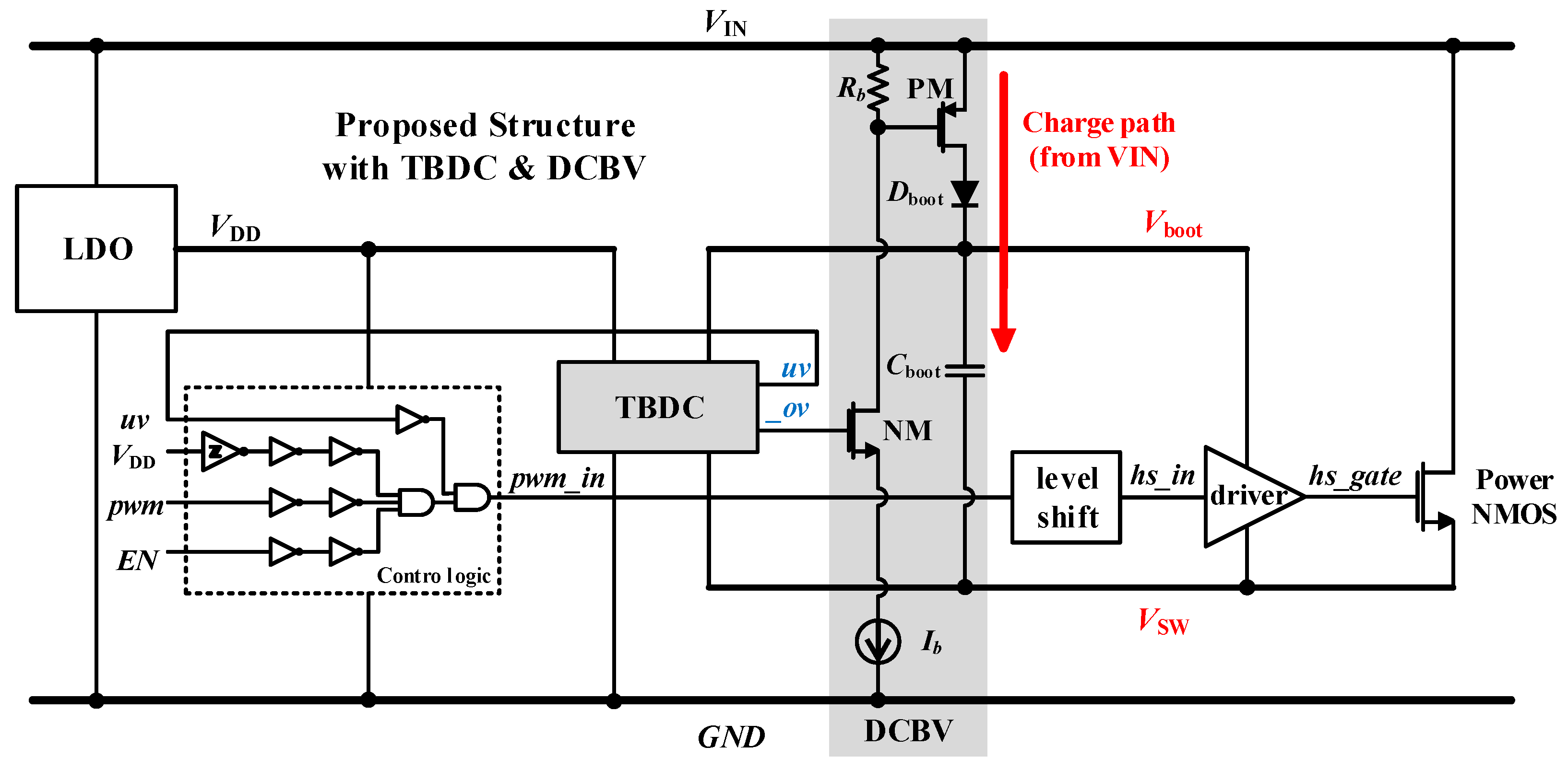
2.1. Concept of the Proposed Bootstrap Architecture

As shown in Figure 2, the DCBV is directly used in the bootstrap charging of the proposed structure, which reduces the pressure on the bandwidth and load capacity of the on-chip LDO at high frequency. The TBDC circuit is used to detect the bootstrap voltage, which is mainly composed of isolated MOSFETs instead of high-voltage devices, and controls the charging path of the bootstrap. Moreover, the logic control module is related to the detection result of the TBDC.
When the TBDC detects that the bootstrap voltage is lower than the under-voltage threshold VTHL, the under-voltage signal uv will pull down the driving signal in the control logic circuit to turn off the power device, thereby avoiding the efficiency loss caused by insufficient driving voltage.
When the TBDC detects that the bootstrap voltage exceeds the over-voltage threshold VTHH, the non-over-voltage signal _ov is set to 0, and the gate of the PMOS switch (PM) is pulled up to VIN by the bias resistor Rb, resulting in the shutdown of PM and charging path. Moreover, the bootstrap voltage slowly decreases until the TBDC detects that the bootstrap is lower than the over-voltage threshold VTHH. Additionally, the _ov signal remains high. The high-voltage NMOS (NM) is turned on, and the bias current Ib causes a voltage drop on the bias resistor Rb. Next, the PM is turned on, and the BUS voltage VIN charges the bootstrap capacitor Cboot through the bootstrap diode Dboot. The charging path is shown as a red arrow, and the bootstrap voltage increases immediately. The above processes are repeated during normal operation. Due to a slight delay in the DCBV circuit, the bootstrap voltage is controlled within a voltage range with a small ripple (VTHH ± ∆V).
In the case of high-frequency operation, the traditional structure has relatively high requirements for the bandwidth and load regulation rate of the LDO. However, the structure designed in this work does not rely on an LDO power supply, which is more suitable for higher frequency.
The working sequence of this circuit is shown in Figure 3.

2.1.1. Power on (Under-Voltage)

When the BUS voltage VIN is powered on, the LDO starts to work, and then the low-voltage power supply VDD increases to 5 V as shown in Figure 3, status ①. The enable signal EN then turns from low to high. At this time, the external input signal pwm is low. The high-side power NMOS remains off, and the switch node VSW is 0. Moreover, the bootstrap voltage is lower than the under-voltage threshold VTHL, and the under-voltage signal uv is the VDD. The uv signal turns off the high-side N-type power device in the control logic circuit.
The _ov signal is also the VDD, so the bootstrap charging path is opened, and the bootstrap voltage increases.

2.1.2. Charging

When the bootstrap voltage increases to the under-voltage threshold VTHL as shown in Figure 3, status ②, the under-voltage signal uv reverses from the VDD to the GND, and the pwm signal can normally control the high-side power NMOS.
Additionally, the _ov signal is still the VDD, and the bootstrap charging path remains open, causing the bootstrap voltage to continue increasing.

2.1.3. Discharging (Over-Voltage)

When the bootstrap voltage exceeds the over-voltage threshold VTHH as shown in Figure 3, status ③, the _ov signal is flipped from the VDD to the GND. Therefore, the charging path is turned off, and the bootstrap voltage slowly decreases.

2.1.4. Repeating (pwm Remains Low)

When the external input signal pwm continues to be low and the bootstrap voltage decreases to less than the over-voltage threshold VTHH as shown in Figure 3, status ④, processes Charging (status ②) and Discharging (status ③) are repeated.

2.1.5. pwm Becoming High

When the external input signal pwm becomes high, the high-side power NMOS is turned on, and the switch node VSW voltage is pulled up to the BUS voltage VIN as shown in Figure 3, status ⑤. At this time, since the voltage at the anode of the bootstrap diode Dboot is the BUS voltage VIN and the voltage at the negative terminal of Dboot is the high-side bootstrap power rail voltage Vboot, the charging path cannot be charged. Additionally, the high-side bootstrap power rail slowly decreases due to the power supply to the high-side driver and the leakage of the bootstrap capacitor Cboot.

2.1.6. pwm Becoming Low

As status ⑥ shows in Figure 3, after the input signal pwm becomes low, processes Charging and Discharging are repeated, which behaves the same as status ④.

2.2. Circuit Realization

The TBDC circuit is used to detect the over-voltage and under-voltage conditions of the bootstrap voltage, which is composed of three parts as shown in Figure 4, including a current bias and start-up circuit, an under-voltage detection circuit, and an over-voltage detection circuit. In addition, level shifter and driver are shown in Figure 5 and Figure 6, respectively.

2.2.1. TBDC Circuit

  • Current bias and start-up circuit
The current bias and start-up circuit are shown in the left part in Figure 4, which are composed of isolated PMOS PM1–PM2, isolated NMOS NM1–NM2, and a resistor R1. PM1 mirrors the current of PM2, and resistor R1 is used to control the magnitude of the bias current. The bias current increases as the bootstrap voltage increases until it stabilizes. The stable bias current is [30]:
I out = 2 μ n C o x ( W / L ) 1 × 1 R 1 2 × ( 1 1 K ) 2
where μ n is the electron mobility of NM1, C o x is the gate-oxide capacitance per unit area, ( W / L ) 1 is the ratio of width and length of NM1, and K is the ratio of NM2 and NM1. The value of I out is set to 1 μA to balance the power consumption and area. The length of NM1 is set to 2 μm so that the channel length modulation effect can be reduced. The value of K is set to 32 and resistance of R1 is about 170 KΩ by calculation. To avoid the degenerate state when the current is 0, a start-up structure is introduced with isolated NMOS NM3–NM4 and isolated PMOS PM3–PM4. When the bias current is 0, the gate-source voltage VGS2 of NM2 is 0 V. At this time, the gate voltages of PM3 and PM4 are 0 V, and they are turned on. Then, the gate of NM3 is pulled high and turned on, and there is current that flows through resistor R1. Therefore, the bias current is not 0, and the degenerate state is eliminated. Once there is flowing current, the gate-source voltage VGS2 of NM2 increases to a value greater than the threshold voltage VTHN, and then NM4 is turned on. Moreover, the gate voltage of NM3 is pulled down, and the start-up circuit is turned off.
  • Under-voltage detection circuit
The under-voltage detection circuit is shown in the middle part of Figure 4, which is composed of isolated PMOS PM5–PM6, isolated NMOS NM5–NM7, resistors R2R3, and a level shifter circuit.
As the bootstrap voltage gradually increases from 0, the bias current Iout rises. PM5 mirrors the current of PM2, and the gate-source voltage VGS5 of PM5 is equal to the VGS2 of PM2. Due to the existence of R3 and PM5, NM6 cannot be turned on immediately at a low current. At this time, the drain voltage of PM6 is pulled up to Vboot. After the first level shifter circuit, the output of the under-voltage signal uv is VDD.
By adjusting the size of PM5, NM5, R2, and R3, the under-voltage threshold VTHL voltage can be set to 2.2 V to ensure a low on-resistance of the power NMOS. When the bootstrap voltage reaches VTHL, which can be expressed as:
V THL = V DSP 5 + V GSN 5 + I out × ( R 2 + R 3 ) + V THN
NM6 and NM7 are turned on, and the drain voltage of NM7 gradually decreases until it is lower than the threshold of the level shifter. At this time, the output of the under-voltage signal uv is GND. In this case, NM5 is assumed to be critical saturation, and V DSP 5 could be set to the overdrive voltage (about 200 mV to 300 mV). V THN is about 900 mV, and V GSN 5 should be larger than threshold voltage. The above data are substituted in equation 2, and then the value of R 2 and R 3 is estimated at about 200 KΩ.
  • Over-voltage detection circuit
Isolated PMOS PM7-PM9, isolated NMOS NM8-NM15, resistors R4-R5, Zener diode DZ, and another level shifter circuit constitute an over-voltage detection circuit, as shown in the right part of Figure 4.
The gate voltage of NM9 is a fixed value when the bias current Iout is determined, which is:
V GN 9 = I out × R 4 + V GSN 8
The source voltage of NM9 is:
V SN 9 = V boot ( V GSN 10 + V GSN 11 + V GSN 12 + V GSN 13 + V GSN 14 ) = V boot 5 × V GSN
Therefore, the gate-source voltage of NM9 is:
V GSN 9 = I out × R 4 + V GSN 8 + 5 × V GSN V boot
When the gate-source voltage of NM9 is lower than VTHN, NM9 will be turned off, and the gate voltage of NM15 will be pulled up to Vboot, while the drain voltage will be pulled low. Therefore, the output of _ov signal is GND after the level shifter circuit. Therefore, the over-voltage threshold is deduced as:
V THH = I out R 4 + 5 × V GSN + V GS 8 V THN
However, there is another device, a Zener diode DZ, used in the over-voltage circuit, which double guarantees _ov signal to be low during its over-voltage. DZ will clamp the source voltage of NM9 through providing enough current when the bootstrap voltage reaches its threshold. At this time, the threshold voltage is:
V THH = V DZ + I out R 4
where V DZ is the clamp voltage of Zener diode.
The constant current of this circuit is set to 1 μA each branch, and the size of PM7 and PM8 is the same as PM1 and PM2. By adjusting the size of NM8, NM10–NM14, and R4, the VTHH voltage is set to 6 V, thereby avoiding the breakdown of the power NMOS.
The TBDC circuit is designed with fully isolated devices due to area consideration, and the bootstrap capacitor is directly charged from the BUS voltage with the DCBV circuit, which can be used for higher frequency. Due to the usage of a digital control method, the bootstrap voltage is stable when VIN varies from 6 V to 48 V; therefore, the line regulation of this circuit can be considered close to 0.

2.2.2. Level Shifters

There are two types of level shifters employed in the proposed bootstrap structure. One is a level-up shifter used to control the power NMOS, and the other is a level-down shifter in the TBDC circuit.
  • Level-up shifter
The pwm_in signal is the output of control logic, and it is 3.3 V or 5 V relative to ground, which is not suitable to control the driver directly. Therefore, the level-up shifter is adopted to shift the voltage relative to ground to the voltage relative to VSW. The level-up shifter used in the proposed structure is illustrated in Figure 5a. HPM1, HPM2, HNM1, and HNM2 are the only high-voltage devices in this circuit, and other devices are low-voltage devices (INV1) or isolated devices (PM11, PM12 and INV2). R7 is a pull-up resistor to ensure the initial condition of hs_in, preventing from floating gate of INV2.
  • Level-down shifter
A level-down shifter is used in the TBDC circuit to shift the uv and _ov signal from floating voltage to voltage relative to ground, so that uv can be an input of control logic and _uv is appropriate for controlling NM in the DCBV. The principle of the level-down shifter is similar to that of the level-up shifter, and the circuit is shown in Figure 5b.

2.2.3. Driver

The driver circuit shown in Figure 6 provides sufficient driving current for the power device through PM10 and NM16. The source and sink current are determined by the gate capacitance CGS of the power device, turn-on/off voltage of the power device and required rising/falling time, and can be adjusted by changing the size of PM10 and NM16. Deadtime is used to prevent the power rail from shooting through, and the waveforms of hs_in, gate of PM10, and NM16 are also shown in Figure 6.

3. Results

The circuit is implemented by the CSMC 0.25 µm 60 V BCD process. Figure 7 shows the micrograph and testbench photos using the proposed bootstrap structure. The chip area is 1.4 × 1.3 mm2, of which the bootstrap circuit only occupies 0.149 mm2. The maximum input voltage can be up to 48 V, and the operating frequency can reach 5 MHz.

3.1. Simulation Results

Figure 8 shows the DC simulation result of the TBDC circuit. When the bootstrap voltage is lower than VTHL (2.101 V), uv and _ov are high. When the voltage is between the VTHL and VTHH (2.101–6.099 V), the uv output is low and the _ov output is high. When the voltage between Vboot and VSW is higher than the VTHH (6.099 V), the uv output is low and the _ov output is low.
The overall and enlarged simulation results are shown in Figure 9a,b. When the pwm is 0 and the bootstrap voltage is higher than VTHH (6 V), the output of the _ov signal is 0 V and NM is turned off. Therefore, there is no voltage drop on the bias resistor Rb, and the voltage of VSGP is 0 V, which causes the charging path to be turned off. When the bootstrap voltage is lower than VTHH, the output of the _ov signal is 5 V and NM is turned on. A voltage drop can be formed on the bias resistor Rb, and the voltage of VSGP can increase to 3 V, causing the charging path to be opened. However, the voltage of VSGP only increases to 3 V instead of 5 V, which can be attributed to the fact that the bootstrap voltage is quickly charged to 6 V by the VIN when the PM is turned on. During this period, the ripple of Vboot-VSW is only 1.583 mV.
The temperature simulation result is shown in Figure 10a. The minimum bootstrap voltage is 5.866 V at −40 °C, and the maximum bootstrap voltage is 6.210 V at 120 °C. The bootstrap voltage is positively correlated with the temperature, and the temperature coefficient is calculated as:
T C = V o u t ( T m a x T m i n ) × V n o m × 10 6 = 348   ppm /
The simulation results for different load currents are shown in Figure 10b, indicating a good load regulation. The maximum bootstrap voltage is 6.210 V at 1 A, and the minimum voltage is 6.208 V at 1 mA. The load regulation S v can be calculated as:
S v = V o u t V n o m × I o u t = 0.03 % / m A
The simulated result of the buck converter at Iload = 1 A configured by this bootstrap structure is shown in Figure 11. The input and output voltages are 14.5 V and 5 V, respectively. The ripple of the output voltage is 2.612 mV with an efficiency of 92.7%. The highest simulated efficiency is 94.87% at 600 mA.

3.2. Test Results

The test result, as shown in Figure 12a, indicates that the voltage power-up time of bootstrap voltage is approximately 170 µs, and the stable voltage is approximately 6 V, which are consistent with the simulation result. The results of different operation frequencies are shown in Figure 12b, indicating good support over a wide frequency range.
A comparison of the simulation and actual measurement results of the buck converter are shown in Figure 13. Under the following conditions, VIN = 14.5 V and VOUT = 5 V, the highest tested efficiency of the circuit is 83.6% (Iload = 400 mA). The figure-of-merit (FOM) is defined as:
FOM = A I load , max × η 0.5
where A is the silicon area, Iload,max is the maximum load, and η is the efficiency at maximum load [31]. For this definition, a low value indicates a better performance and the circuit achieves a good FOM of 0.074. Due to diode conduction loss, MOS conduction loss, and MOS switching loss, there is a certain gap between the simulation results and the actual measurement results.

4. Discussion

Table 1 shows the comparison results between the structure designed in this paper and those reported in previous literature. Compared with the previous research, this work has the advantages of a wider input voltage from 3.6 V to 48 V, higher switching frequency up to 5 MHz, larger output current of 2.7 A, and a smaller chip area of 1.82 mm2 with a good FOM of 0.074 while maintaining the same efficiency. With the digital control method being different from previous research, the simulation and test result implicate that the novel DCBV and TBDC methods in the proposed bootstrap structure is feasible and stable. The proposed circuit can be applied to some power areas such as dc–dc converters.
However, due to the lack of research on temperature compensation, the temperature coefficient of this structure is not as low as traditional LDOs. Therefore, future research on this circuit include decreasing the temperature coefficient and scaling higher power.

5. Conclusions

Bootstrap is a key structure for driving and protecting a high-side N-type power device. In this paper, a novel bootstrap circuit has been proposed, which is directly charged by the BUS voltage and employs a digital method to achieve a stable output. With an area of 1.82 mm2, this structure exhibits strict voltage control in a wide range of input voltages and frequencies. It is found that when using the dc–dc asynchronous buck converter, the maximum efficiency of the protype is 83.6%, and the FOM is 0.074, showing its future potential in a wide range of scenarios, such as in power converters, motor drivers, and automobiles.

Author Contributions

Conceptualization, Y.G. and F.Y.; methodology, Y.G. and F.Y.; software, Y.G., Y.C., and Y.K.; validation, Y.G., F.Y., and X.Z.; formal analysis, Y.G. and Y.C.; investigation, Y.G. and Y.K.; resources, X.Z.; data curation, Y.G.; supervision, F.Y. and X.Z.; writing—original draft preparation, Y.G.; writing—review and editing, Y.G. and F.Y.; project administration, F.Y. and X.Z.; funding acquisition, X.Z. All authors have read and agreed to the published version of the manuscript.

Funding

This research was supported by the Science and Technology Service Network Initiative of CAS (No. KFJ-STS-QYZX-099).

Acknowledgments

I would like to thank Huan Wang, Shuo Wang, Libo Zhang, and Kun Lin at Advanced Semiconductors of Intelligences and Technologies, Haining, China for helping in the wire bonding and chip test.

Conflicts of Interest

The authors declare no conflict of interest.

References

  1. Weckbrodt, J.; Ginot, N.; Batard, C.; Le, T.L.; Azzopardi, S. A Bidirectional Communicating Power Supply Circuit for Smart Gate Driver Boards. IEEE Trans. Power Electron. 2020, 35, 8540–8549. [Google Scholar] [CrossRef]
  2. Zhang, Y.; Rodriguez, M.; Maksimovic, D. Very High Frequency PWM Buck Converters Using Monolithic GaN Half-Bridge Power Stages with Integrated Gate Drivers. IEEE Trans. Power Electron. 2016, 31, 7926–7942. [Google Scholar] [CrossRef]
  3. Ye, Z.C.; Lei, Y.T.; Liu, W.-C.; Shenoy, P.S.; Pilawa-Podgurski, R.C.N. Improved Bootstrap Methods for Powering Floating Gate Drivers of Flying Capacitor Multilevel Converters and Hybrid Switched-Capacitor Converters. IEEE Trans. Power Electron. 2019, 35, 5965–5977. [Google Scholar] [CrossRef]
  4. Nguyen, V.-S.; Lefranc, P.; Crebier, J.-C. Gate Driver Supply Architectures for Common Mode Conducted EMI Reduction in Series Connection of Multiple Power Devices. IEEE Trans. Power Electron. 2018, 33, 10265–10276. [Google Scholar] [CrossRef]
  5. Ranganathan, S.; Mohan, A.N.D. Formulation and Analysis of Single Switch High Gain Hybrid DC to DC Converter for High Power Applications. Electronics 2021, 10, 2445. [Google Scholar] [CrossRef]
  6. Garza-Arias, E.; Rosas-Caro, J.C.; Valdez-Resendiz, J.E.; Mayo-Maldonado, J.C.; Escobar-Valderrama, G.; Guillen, D.; Rodríguez, A. The Fourth-Order Single-Switch Improved Super-Boost Converter with Reduced Input Current Ripple. Electronics 2021, 10, 2379. [Google Scholar] [CrossRef]
  7. Aksin, D.; Al-Shyoukh, M.A.; Maloberti, F. A bootstrapped switch for precise sampling of inputs with signa range beyond supply voltage. In Proceedings of the IEEE 2005 Custom Integrated Circuits Conference (CICC 2005), San Jose, CA, USA, 21 September 2005. [Google Scholar]
  8. Lima, J.A.D.; Pimenta, W.A. A current-mode active clampling for boostrap circuit applied to DC/DC buck converters. In Proceedings of the 2009 IEEE International Symposium on Circuits and Systems (ISCAS 2009), Taipei, Taiwan, 24–27 May 2009. [Google Scholar]
  9. Zhou, Z.; Ming, X.; Zhang, B.; Li, Z. Design of Novel Bootstrap Driver Used in High Power BUCK Converter. In Proceedings of the 2009 IEEE 8th International Conference on ASIC (ASICON 2009), Changsha, China, 20–23 October 2009. [Google Scholar]
  10. Mudanai, S.; Chindalore, G.; Shih, W.-K.; Wang, H.; Tasch, A.F., Jr.; Mazar., C.M. Temperature characterization and modeling of electron and hole mobilities in MOS accumulation layers. In Proceedings of the 56th Annual Device Research Conference Diges (DRC, 1998), Charlottesville, VA, USA, 22–24 June 1998; pp. 20–21. [Google Scholar]
  11. Seo, D.W.; Choi, H.G.; Twynam, J.; Kim, K.M.; Yim, J.S.; Moon, S.-W.; Jung, S.; Lee, J.; Roh, S.D. 600 V-18 A GaN Power MOS-HEMTs on 150 mm Si Substrates with Au-Free Electrodes. IEEE Electron. Device Lett. 2014, 35, 446–448. [Google Scholar] [CrossRef]
  12. Kanamura, M.; Ohki, T.; Kikkawa, T.; Imanishi, K.; Imada, T.; Yamada, A.; Hara, N. Enhancement-Mode GaN MIS-HEMTs with n-GaN/i-AlN/n-GaN Triple Cap Layer and High- $k$ Gate Dielectrics. IEEE Electron. Device Lett. 2010, 31, 189–191. [Google Scholar] [CrossRef]
  13. Zheng, J.X.; Ma, X.H.; Lu, Y.; Zhao, B.C.; Zhang, H.S.; Zhang, M.; Hao, Y. A Scalable Active Compensatory Sub-Circuit for Accurate GaN HEMT Large Signal Models. IEEE Microw. Wirel. Compon. Lett. 2016, 26, 431–433. [Google Scholar] [CrossRef]
  14. Rossetto, I.; Meneghini, M.; Hilt, O.; Bahat-Treidel, E.; De Santi, C.; Dalcanale, S.; Wuerfl, J.; Zanoni, E.; Meneghesso, G. Time-Dependent Failure of GaN-on-Si Power HEMTs with p-GaN Gate. IEEE Trans. Electron. Devices 2016, 63, 2334–2339. [Google Scholar] [CrossRef]
  15. Huang, M.; Lu, Y.; Martins, R.P. Review of Analog-Assisted-Digital and Digital-Assisted-Analog Low Dropout Regulators. IEEE Trans. Circuits Syst. II Express Briefs 2021, 68, 24–29. [Google Scholar] [CrossRef]
  16. Ballo, A.; Grasso, A.D.; Palumbo, G. A simple and effective design strategy to increase power conversion efficiency of linear charge pumps. Int. J. Circuit Theory Appl. 2019, 48, 157–161. [Google Scholar] [CrossRef]
  17. Ballo, A.; Grasso, A.D.; Palumbo, G.; Tanzawa, T. Linear distribution of capacitance in Dickson charge pumps to reduce rise time. Int. J. Circuit Theory Appl. 2020, 48, 555–566. [Google Scholar] [CrossRef]
  18. Ballo, A.; Grasso, A.D.; Palumbo, G. Current-mode body-biased switch to increase performance of linear charge pumps. Int. J. Circuit Theory Appl. 2020, 48, 1864–1872. [Google Scholar] [CrossRef]
  19. Grobe, J.; Hanhart, M.; Maul, F.; Weihs, L.; Rolff, L.; Wunderlich, R.; Heinen, S. Design of a Flexible Bandgap Based High Voltage UVLO with Pre-Regulator. In Proceedings of the 2020 27th IEEE International Conference on Electronics, Circuits and Systems (ICECS 2020), Glasgow, UK, 23–25 November 2020. [Google Scholar]
  20. Park, S.; Jahns, T.M. A self-boost charge pump topology for a gate drive high-side power supply. IEEE Trans. Power Electron. 2005, 20, 300–307. [Google Scholar] [CrossRef] [Green Version]
  21. Xin, Z.; Zhigang, L.; Huang, A. A High-Dynamic Range Current Source Gate Driver for Switching-Loss Reduction of High-Side Switch in Buck Converter. IEEE Trans. Power Electron. 2010, 25, 1439–1443. [Google Scholar]
  22. Yuan, B.; Ying, J.; Ng, W.T.; Lai, X.-Q.; Zhang, L.-F. A High-Voltage DC–DC Buck Converter with Dynamic Level Shifter for Bootstrapped High-Side Gate Driver and Diode Emulator. IEEE Trans. Power Electron. 2020, 35, 7295–7304. [Google Scholar] [CrossRef]
  23. Kong, M.; Yan, W.; Li, W. Design of a synchronous-rectified buck bootstrap MOSFET driver for voltage regulator module. In Proceedings of the 2007 7th International Conference on ASIC (ASICON 2007), Guilin, China, 22–25 October 2007. [Google Scholar]
  24. Abe, K.; Nishijima, K.; Harada, K.; Nakano, T.; Nabeshima, T.; Sato, T. A Novel Three-Phase Buck Converter with Bootstrap Driver Circuit. In Proceedings of the 2007 IEEE Power Electronics Specialists Conference (PESC 2007), Orlando, FL, USA, 17–21 June 2007. [Google Scholar]
  25. Yuan, B.; Xiao, L.-Q.; Wang, B.-Y.; Ying, J. High-Speed Dynamic Level Shifter for High-Side Bootstrapped Gate Driver in High-Voltage Buck Regulators. IEEE Trans. Circuits Syst. II Express Briefs 2021, 68, 3083–3087. [Google Scholar] [CrossRef]
  26. Li, S.T.; Wang, P.Y.; Chen, C.J.; Hsu, C.C. A 10MHz GaN Driver with Gate Ringing Suppression and Active Bootstrap Control. In Proceedings of the 2019 IEEE Workshop on Wide Bandgap Power Devices and Applications in Asia (WiPDA Asia), Taipei, Taiwan, 23–25 May 2019. [Google Scholar]
  27. Ke, X.; Sankman, J.; Song, M.K.; Forghani, P. 16.8 A 3-to-40V 10-to-30MHz automotive-use GaN driver with active BST balancing and VSW dual-edge dead-time modulation achieving 8.3 improvement and 3.4ns constant propagation delay. In Proceedings of the IEEE International Solid-State Circuits Conference, San Francisco, CA, USA, 31 January–4 February 2016. [Google Scholar]
  28. Ming, X.; Fan, Z.; Xin, Y.; Zhang, X.; Shi, F.; Pan, S.; Zhang, J.; Wang, Z.; Zhang, B. An Advanced Bootstrap Circuit for High Frequency, High Area-Efficiency and Low EMI Buck Converter. IEEE Trans. Circuits Syst. II Express Briefs 2019, 66, 858–862. [Google Scholar] [CrossRef]
  29. Liu, Y.; Liu, S.; Ye, Q.; Yuan, B.; Lai, X. A feedback loop regulated bootstrap driver circuit with improved drive capability for high voltage buck DC–DC converter. Microelectron. J. 2013, 44, 1290–1295. [Google Scholar] [CrossRef]
  30. Razavi, B. Bandgap Reference. In Dsign of Analog CMOS Integrated Circuits, 2nd ed.; McGraw-Hill: New York, NY, USA, 2017; pp. 510–512. [Google Scholar]
  31. Chen, W.-C.; Chou, Y.-W.; Chien, M.-W.; Chen, H.-C.; Yang, S.-H.; Chen, K.-H.; Lin, Y.-H.; Lee, C.-C.; Lin, S.-R.; Tsai, T.-Y. A Dynamic Bootstrap Voltage Technique for a High-Efficiency Buck Converter in a Universal Serial Bus Power Delivery Device. IEEE Trans. Power Electron. 2016, 31, 3002–3015. [Google Scholar] [CrossRef]
  32. Seidel, A.; Costa, M.S.; Joos, J.; Wicht, B. Area Efficient Integrated Gate Drivers Based on High-Voltage Charge Storing. IEEE J. Solid-State Circuits 2015, 50, 1550–1559. [Google Scholar] [CrossRef]
Figure 1. Traditional bootstrap structure charging from an LDO, which brings bandwidth and stability pressure to LDO.
Electronics 10 02863 g001
Figure 2. Proposed bootstrap structure with TBDC and DCBV.
Electronics 10 02863 g002
Figure 3. Working sequence of the proposed bootstrap structure.
Electronics 10 02863 g003
Figure 4. Circuit realization of the proposed TBDC with fully isolated devices.
Electronics 10 02863 g004
Figure 5. Circuit realization of (a) level-up shifter and (b) level-down shifter employed in proposed structure.
Electronics 10 02863 g005
Figure 6. Circuit realization of driver and waveforms of hs_in, gate of PM10 and NM16.
Electronics 10 02863 g006
Figure 7. Chip micrograph and testbench of the buck converter with the proposed bootstrap circuit.
Electronics 10 02863 g007
Figure 8. Simulated DC under-voltage and over-voltage threshold of TBDC.
Electronics 10 02863 g008
Figure 9. Simulated results of the proposed bootstrap structure: (a) overall result and (b) enlarged result.
Electronics 10 02863 g009
Figure 10. Simulation result at (a) different temperature (T = −40 °C, 0 °C, 40 °C, 80 °C and 120 °C) and (b) different load current (1 μA and 1 mA).
Electronics 10 02863 g010
Figure 11. Simulation results of buck converter (VIN = 14.5 V, VOUT = 5 V, Iload = 1 A).
Electronics 10 02863 g011
Figure 12. Measured bootstrap circuit (external Cboot = 1 μF) (a) power on and stable state, and (b) bootstrap voltage at pwm = 0 Hz, 1 MHz, and 5 MHz.
Electronics 10 02863 g012
Figure 13. Comparison between the simulated and test results of the buck converter efficiency at different currents (VIN = 14.5 V, VOUT = 5 V).
Electronics 10 02863 g013
Table 1. Comparison with previously published works is shown, indicating wider input voltage, higher switching frequency, larger output current, and smaller chip area with a good FOM while maintaining the same efficiency.
ParameterThis WorkRef [23]Ref [32]Ref [22]
Technology
(µm)
0.25 µm 60 V BCD0.35 µm 40 V CMOS0.18 µm HV
BiCMOS
0.35 µm HV BCD
Input voltage
VIN (V)
3.6–483.6–36153–40
Switching
frequency (MHz)
0.1–50.2–2.4210–30
Output current (A)2.722.61.2
Efficiency η (%)83.685.98N/AN/A
Chip area A (mm2)1.824.78N/AN/A
Bootstrap circuit area (mm2)0.1490.0620.420.48
Dropout voltage (mV)1.583
(simulation)
4.6
(simulation)
N/AN/A
LDO typeCaplessCaplessExternal capN/A
FOM (A/Iload,max×η0.5)0.0740.258N/AN/A
Bootstrap rail
control
TBDCDVSN/AABB
Publisher’s Note: MDPI stays neutral with regard to jurisdictional claims in published maps and institutional affiliations.

