
Reconfigurable Morphological Processor for Grayscale Image Processing


School of Software, Xi’an Jiaotong University, Xi’an 710049, China
Electronics 2021, 10(19), 2429; https://doi.org/10.3390/electronics10192429
Submission received: 31 August 2021
/
Revised: 28 September 2021
/
Accepted: 29 September 2021
/
Published: 7 October 2021
(This article belongs to the Special Issue Design Tools and Architectures for Coarse-Grained Reconfigurable Computing)
Abstract
:Grayscale morphology is a powerful tool in image, video, and visual applications. A reconfigurable processor is proposed for grayscale image morphological processing. The architecture of the processor is a combination of a reconfigurable grayscale processing module (RGPM) and peripheral circuits. The RGPM, which consists of four grayscale computing units, conducts grayscale morphological operations and implements related algorithms of more than 100 f/s for a 1024 × 1024 image. The periphery circuits control the entire image processing and dynamic reconfiguration process. Synthesis results show that the proposed processor can provide 43.12 GOPS and achieve 8.87 GOPS/mm2 at a 220-MHz system clock. The simulation and experimental results show that the processor is suitable for high-performance embedded systems.
1. Introduction
Mathematical morphology is extensively used in various areas, such as computer vision and machine learning [1], texture and image analysis [2,3], color image processing [4], remote sensing image analysis [5], image compression [6], and video segmentation [7]. Morphological computing has commonly been implemented using processors such as CPU or DSP. Some enhancements were implemented on GPUs to speed up the process [8,9,10]; however, even high-end GPUs have lower throughput than CPUs and FPGAs [11], and GPUs are more expensive with a higher power consumption for embedded systems. Therefore, high-speed specialized image processing chips have received considerable attention due to their efficient performance and low power consumption. Partial-result-reuse (PRR) architecture, as proposed in [12], has been used for morphological operations and can be combined with systolic array architecture to enhance performance and maintain cost-efficiency. Pipeline architecture for morphological operations has been presented to reduce computing latency. A 2D stream, processing architecture, was implemented on Virtex-5 for sequential filters [13]. An algorithm for efficient computation of morphological operations and specific hardware were presented in [14]. A hardware architecture presented for gray-level image erosion and dilation utilized a systolic-like organization of processing elemental array [15].
With technological advances, mathematical morphology continues to be introduced to new applications and the algorithms improve and expand constantly. Flexibility is important in image processing chips. Thus, the reconfigurable technique and processing element array architecture, which can solve the incompatibility between high performance and flexibility, are used in morphological image processing chips. A content-addressable memory (CAM) LSI for real-time pixel-parallel image processing was described in [16]. A programmable single-instruction multiple-data (SIMD) real-time vision chip was reported to achieve high-speed target tracking [17]. Recently, a vision chip with the architecture of a massively parallel cellular array of processing elements was reported for image processing using the asynchronous or synchronous processing technique [18]. In [7], a reconfigurable morphological image processing accelerator was proposed for video object segmentation, and watershed transform could be achieved in real time using 32 macro processing elements.
A high-performance flexible reconfigurable processor that can conduct basic grayscale morphological operations and implement complicated algorithms is presented. The processor consists of a morphology processing module and peripheral circuits. The morphology processing module is a reconfigurable hardware accelerator for grayscale morphological operations, which can deal with the arbitrary size and shape of structure elements (SEs). The accelerator is a mixed-grained architecture, which has novelty maximum and minimum computing circuits and a high flexibility and efficiency structure. The operation can be reconfigured dynamically and the peripheral circuits can select and synchronize the input and output images. The processor can be designed easily and achieve an optimal hardware cost. The processor can process pixel-level images and extract image features, such as boundary and gradient. The processor is high speed, with a simple structure, and an extensive application range.
This paper is organized as follows. A literature review is present in Section 2. The maximum and minimum computing circuits, which are the key units of the morphological operations, are introduced in Section 3. The processor architecture is presented in Section 4. The processor implementation and algorithms involved in image processing by the processor are described in Section 5. In Section 6, the performance of the processor is evaluated and compared with that of existing processors. Finally, the discussion and conclusion is provided in Section 7.
2. Literature Review
In recent years, image and vision applications are widely used in advanced manufacturing, medicine, national defense, public safety, and space technology; however, the traditional CPU and ASIC cannot provide both high performance and enough flexibility, which limits the development and application of the systems. In order to improve performance, GPU-based parallel algorithms are designed in [19,20]. FPGA is also a good platform for high-performance systems [21,22]; however, the GPU and FPGA still do not solve the problem of flexibility and performance in image processing and machine vision. Reconfiguration, which can solve the problem, is introduced to realize high-flexibility and performance chips.
Several reconfigurable chips have realized general computing tasks through PE array, based on SIMD structure. Thus, chips with multi reconfigurable cores which are connected in a high-performance manner (such as NoC) will be the trend. Some NPUs use reconfigurable computing units to improve flexibility [23,24,25,26]. When implementing reconfigurable precisions, compute-in-memory macro is fully reconfigurable in [27,28] and some chips used for IoT [29] and Biomedical AI Processor [30].
In addition, in order to meet the requirements of general computing, it is necessary to study the general reconfigurable chip, and pay attention to the problems of software framework, auxiliary compilation, and task scheduling. The calculation model and algorithm research provide the basis for the architecture design of the reconfigurable chip.
3. Maximum and Minimum Computing Circuits
3.1. Morphological Operations
The basic morphological operations are dilation and erosion. For a 2D grayscale image, A is the image and B is the SE. The flat dilation, which is denoted by , is computed using the following equation:
where α and β are the domain of the SEs. Erosion, which is denoted by , can be computed using the following equation:
The combinations of dilation and erosion can form other morphological operations. The opening and closing operations, denoted by and , are expressed as follows:
The computation of a maximum and minimum value is the key operation for grayscale morphological operations. The design of the maximum and minimum computing circuits directly affects the performance of the morphological processor.
3.2. Algorithms of the Maximum and Minimum Computing
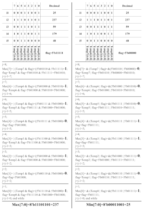
In this study, we implemented maximum and minimum computing by logic operations instead of comparators and delay elements. This new method reduces hardware resources. The maximum and minimum computing methods were proposed in [31]. The algorithms used were for the systolic array architecture. We modified the maximum and minimum computing for grayscale morphological operations, and the methods are described in Algorithms 1 and 2, respectively. In Algorithm 1, m n-bit numbers are maximized. All bits of an m-bit parameter, which is denoted by a flag, are set to “1”. The n m-bit parameters, which are denoted by Temp(n − 1), Temp(n − 2), …, Temp0, are marked as the i-bit of all numbers. For example, Temp0 is the combination of i1[0], i2[0], …, im[0]. Line 1 initializes the number of loops. Lines 3 to 5 calculate the maximum number of inputs. The minimum computing method is described in Algorithm 2. The flag is set to “0”. An example is shown in Figure 1. Five 8-bit numbers, namely, 25, 237, 59, 179, and 48, are the inputs. Flags are set to “11111” and “00000” for maximum and minimum computing, respectively. Each loop is based on Algorithms 1 and 2. Finally, the maximum is 237 and the minimum is 25. The new algorithms proposed in this study are resource-light and easily extensible.
| Algorithm 1 Maximum computing. |
|
| Algorithm 2 Minimum computing. |
|
3.3. Maximum and Minimum Computing Circuits
The optimized circuit, which implements Algorithm 1 for the maximum computing of eight 8-bit numbers, is shown in Figure 2. The gate count of an n m-bit number computing circuit is computed as: Gate count = 4 × n × (m − 1) − 1. Two gates are used to implement the equation in [31]: . Then, each eight 8-bit numbers’ maximum computing circuit uses 112 gates fewer than in [31]. Four maximum computing circuits are synthesized with the Synopsys Design Compiler. The synthesis results of various input circuits are shown in Table 1. Due to the increase in the critical path and fan-in, the frequency of the circuit is decreased when the input number increases. This section may be divided by subheadings. It should provide a concise and precise description of the experimental results, their interpretation, as well as the experimental conclusions that can be drawn. The minimum computing circuit is implemented in my previous work [32].
4. Architecture
The grayscale image processor is designed for various applications in computer vision, image analysis, medical image processing, and video segmentation systems. Such systems, especially embedded ones, should have high flexibility and performance for extensive applications, and the design focus should be on flexibility and speed. Then, a reconfigurable grayscale image processor with high speed and a simple structure is designed for extensive use and consumption of fewer hardware resources. The architecture is illustrated in Figure 3. The core of the processor is the reconfigurable grayscale processing module (RGPM). The processor also has two bus interfaces, an input control logic unit, an output control logic unit, a process control unit, and a configuration register group. The RGPM performs the image processing. The two bus interfaces connect the processor to the system bus when a SoC is constructed.
The input control logic unit controls the inputs from video images and SDRAM, and registers to the RGPM. The output control logic unit writes the selected parallel image data from the RGPM into SDRAM through bus interface 1. The process control unit reads the configuration information in the configuration registers and controls the operation process of the RGPM. It also controls the input and output control logic units and bus interfaces in data access. After the processed image data are written to SDRAM, the process control unit transmits interrupt requests to complete the interaction of the processor with external systems.
The configuration register group is an extremely important part in the proposed processor. It contains control parameters, reconfiguration information, operation parameters and interaction information. Most of the registers in the configuration register group are written by an external CPU via the system bus, and the rest are written by the internal modules in the proposed processor.
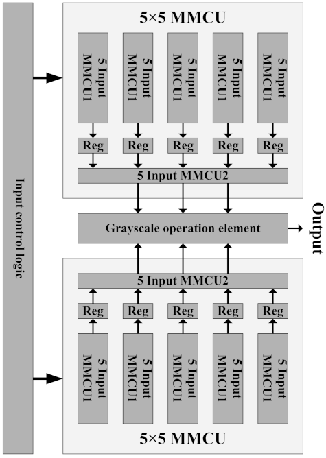
4.1. RGPM
The diagram of the RGPM is shown in Figure 4. The RGPM consists of several grayscale computing units (GCUs) that conduct grayscale morphological operations at a high speed. The image processing algorithms are implemented using the operations in the individual GCUs and the connection pattern of these units. The units can be implemented in a pipelined or parallel manner. The converters select the output from all the GCU outputs based on the parameters and convert the 8-bit data series into a 32-bit data series.
Considering the hardware resource, flexibility, and usability of the processor, we set the number of GCUs to 4. The unit contains two converters. The inputs of GCUs 1 to 4 are the outputs of the input control logic.
4.2. GCU
The architecture of the GCU is shown in Figure 5. The core of the GCU has two 5 × 5 maximum and minimum computing units (MMCUs). The GCU also has one grayscale operation element and one input control logic. The grayscale operation element can conduct 8-bit integer operations, such as two-input maximum, two-input minimum, shifting, complement, addition/subtraction, and straight-through output. This element can be used to supported operations between images.
4.2.1. Input Control Logic
Image signals should be synchronized by the input control logic before being used as input for the MMCUs because one-to-one matching is needed between the pixels in different images. The input control logic selects and synchronizes the inputs from video images and SDRAM to the synchronization circuit. The block diagram of the input control logic is shown in Figure 6. The unit contains 4 data converters, 1 synchronization circuit, 8 line memories and 50 registers. Data converters 1 and 2 convert 8-bit image signals into 32-bit parallel data, which have the same format as the data from SDRAM. Converters 3 and 4 convert the 32-bit data into 8-bit image signals, which are then synchronized by the synchronization circuit. The line memories are needed to buffer the processing image signals. When the size of the SE is n × n, the number of the line buffers is n-1. The depth of each line buffer is the number of the image line pixels, and the width is the pixel intensity (8-bit usually). The n-1 line buffers and the current line video signals create an n-line parallel image input. The n × n pixel registers form an n × n image window. The outputs of line memories are selected by the multiplexers (MUXs) as inputs for the registers, and the image data in the registers are selected as inputs for the MMCU1.
The inputs and outputs of the registers are transmitted via MUXs, which renders the architecture unit more flexible. The inputs transmitted to the MMCUs via MUXs can be reconfigured to two 5 × 5 arrays or one 7 × 7 array. The outputs of the registers transmitted via MUXs can be reconfigured to a 3 × 3, 5 × 5, or 7 × 7 array.
4.2.2. MMCU
The algorithms and circuits of maximum and minimum computing have been presented. The circuit was easy to design and extend. The problem considered was the input number of the MMCU. More inputs meant the consumption of fewer hardware resources, albeit, at a low speed. For example, different circuits, which consist of different input number circuits, are implemented for 5 × SE computing. The implementation results are presented in Table 2. The design of MMCU focuses on the trade-off between resource and frequency. In this study, we selected the five-input MMCU as the basic computing element. For enhancing flexibility, the sixth MMCU (five-input MMCU2) was different from the others, as shown in Figure 7. The implemented operations on the 5 × 5 MMCU were predetermined by configurable registers, including operation parameters, image resolution parameters, mask sizes, input and output selection parameters, and auxiliary parameters.
4.2.3. Reconfiguration and Grayscale Image Processing Operations
Basic morphology operations in the GCU are discussed in this subsection. The following examples are given to illustrate the reconfiguration of the GCU. The GCU can be configured into different structures and conduct basic morphological operations. In Figure 8a, one 5 × 5 MMCU is configured to implement a 5 × 5 operation (the ParaMUX[1] = 1’b1 and Para5 × 5 MMCU1 = 1’b1). The SE is a 5 × 5 square (ParaSE1). The other SE is configured to implement two 3 × 3 operations (the ParaMUX[0] = 1’b0 and Para5 × 5 MMCU2 = 1’b0). The SEs are two 3 × 3 squares (ParaSE2). Therefore, two 5 × 5, one 5 × 5 and two 3 × 3, or four 3 × 3 operations can be conducted on a GCU simultaneously. The maximum operation implemented on a GCU is 7 × 7 (the ParaMUX[2] = 1’b1, Para5 × 5 MMCU1 = 1’b1, and Para5 × 5 MMCU2 = 1’b1). The SE is a 7 × 7 square (ParaSE1 and ParaSE2). The implementation is presented in Figure 8b.
Some grayscale image operations, including flat dilation, erosion, opening, and closing, are given to demonstrate the flexibility of the GCU. The actual use of the GCU is not confined to the examples. The implementation of the operations is shown in Figure 9. The dynamic reconfiguration approach, which allows the reconfiguration to execute at run-time, is employed in the proposed processor. Therefore, the processor can transform the structure using different configurations as they are needed. Thus, the reconfigurable hardware will fit in more applications.
4.2.4. Expansibility
The architecture of the RGPM has good expansibility. Large, processed images can be supported by increasing the depth of the line memories. In this study, the line memories for each GCU are 8-line memories with a length of 1024. For larger image processing, the depth of the line memories can be increased. For example, if the maximum horizontal image size is 1920, then the line memory can be 8 × 1920 × 8 bits. For larger SEs, the number of the line memories can be increased. For example, if the SE size is 31 × 31, then the line memory can be 30 × 1024 × 8 bits. For low hardware consumption, the number of GCUs can be decreased. For higher performance, the number of GCUs can be increased.
5. Implementation
5.1. Synthesis Results
The proposed grayscale image processor was synthesized with the Synopsys Design Compiler and the SMIC0.18 μm cell library. The maximum size of the image to be processed was 1024 × 1024. The maximum size of the mask was 13 × 13. The number of GCUs was 4. The reconfiguration parameter was 24 × 32 bits. The synthesis results are reported in Table 3.
5.2. Grayscale Image Processing Applications
An embedded grayscale image processing system with the proposed processor is presented in Figure 10. The Gaisler Research Leon 2 was selected as the system CPU. The AHB and APB were selected as the system buses. The CPU was used as the controller. The Register group 2 and Interrupt controller were used to control the system. The SDRAM1 and SDRAM2 were used as the main memory source and to store images, respectively. Register group 1 contains control, reconfiguration, and operation parameters (such as morphology operation, image resolution, mask sizes, input and output selection parameters, and auxiliary parameters), and interaction information. It can be written by the CPU via the bus. The control logic reads the parameters in Register group 1; it controls the operation process of the RGPM. It also controls the input and output control logic units and bus interfaces during data access.
The CPU changed the control registers in Register group 2 when the processor was reconfigured. All the parameters needed to be changed for the processor reconfiguration were transferred from the SDRAM1 to the Register group 1 by the bus interface, and then the control registers were changed according to the parameters in Register group 1. After the registers were modified, a signal was transmitted to Register group 2. Then, the reconfiguration was complete; the image processing task was executed. After the processed image data were written to SDRAM, the control logic transmits interrupted requests to complete the interaction.
Some grayscale morphological operations and algorithms are provided to show the high flexibility and performance of the processor.
5.2.1. Basic Mathematical Morphological Operations
5.2.2. Applications
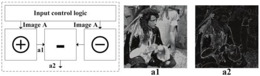
Some example tasks are also implemented for the proposed processor. The hit-and-miss operation, denoted by , is expressed as
Thinning and thickening, denoted by and , are expressed as follows:
The gradient, denoted by , is expressed as follows:
The white top-hat transform is expressed as follows:
6. Performance and Comparison
The grayscale image processing system, as shown in Figure 10, was applied to verify the proposed processor. The operations and tasks, as discussed in Section 4, were applied to the system. The system performance is presented in Table 4. The table shows that the frame rate of operations is more than 200 f/s, and the performance can be multiplied by parallel processing. At a 220 MHz system clock, each GCU in the processor can provide 10.78 GOPS. The entire RGPM containing four GCUs can provide 43.12 GOPS and achieve 8.87 GOPS/mm2 area efficiency (the cell area of the RGPM is 4.86 mm2).
The processor is compared with the processors introduced in [12,13,14,15]. The power consumption of the processor in [12] is normalized to 0.18 μm. The technology scaling of power is expressed as follows:
where L1 and L2 are the characteristic lengths of two different processes. The area is normalized into the number of gates to compare the implementation of the FPGAs and chips, where Countgate = 12 × CountALUT. The summary of hardware features and comparison with related studies [12,13,14,15] are shown in Table 5. The morphological filter in [13] shows the highest performance and the performance can be multiplied by pipelining the filters; however, the hardware resource is too large. The processors in our study and [12] exhibit higher performance per K-gates than the processors used in [13,14,15]. Our processor yields a higher area/pixel ratio than the processors used in [12,15], and yields a higher power/pixel ratio than the processor used in [12]. However, the chip in [12] can only conduct dilation with a 5 × 5 disk SE and the chip in [15] can only conduct 7 × 7 dilation or erosion. The hardware in [12,15] is inflexible for embedded applications; therefore, compared with other processors, our processor, which features a small area, low power consumption, and high flexibility, is more suitable for embedded systems.
The architecture comparison shows that the ASIC and pipeline have a small area and low power consumption. However, inflexibility and low overall performance are inevitable defects of the embedded image processing system. The reconfigurable MIMD array has high performance and flexibility, which is suitable for use in embedded systems for processing large images. The basic operations supported by the processors are shown in Table 6. The hardware in [13] supports dilation, erosion, opening, and closing, but not hit-and-miss and operations between images. This feature limits usage but is efficient for specific applications. As shown in Table 6, our extensively used processor is more suitable for embedded image processing systems.
7. Conclusions
In this study, a reconfigurable grayscale image processor was proposed to conduct high-performance grayscale image morphological processing. The processor consisted of an RGPM and peripheral circuits. The RGPM had a reconfigurable architecture with high performance and flexibility. The maximum and minimum computing circuits, used in RGPM, were employed because of low power consumption and the presence of a small area. Basic morphological operations and complicated algorithms can be implemented easily because of its simple structure. The processor, which has high performance and flexibility, simple structure, and extensive application range, is suitable for embedded image processing systems.
The experimental results demonstrate that each GCU in the processor provided 10.78 GOPS and the grayscale image processor can provide 43.12 GOPS and achieve 8.87 GOPS/mm2 area efficiency at a 220 MHz system clock. Compared with other processors, our processor is more suitable for embedded image processing systems.
Funding
This research was supported by the Fundamental Research Funds for the Central Universities and Science and Technology Plan in Xi’an (201809162CX3JC4).
Conflicts of Interest
The authors declare no conflict of interest.
References
- Marquez-Neila, P.; Baumela, L.; Alvarez, L. A Morphological Approach to Curvature-Based Evolution of Curves and Surfaces. IEEE Trans. Pattern Anal. Mach. Intell. 2014, 36, 2–17. [Google Scholar] [CrossRef] [PubMed]
- Boato, G.; Dang-Nguyen, D.; de Natale, F.G.B. Morphological Filter Detector for Image Forensics Applications. IEEE Access 2020, 8, 13549–13560. [Google Scholar] [CrossRef]
- Lu, Q.; Hu, X. Hyperspectral Image Classification via Exploring Spectral–Spatial Information of Saliency Profiles. IEEE J. Sel. Top. Appl. Earth Obs. Remote Sens. 2020, 13, 3291–3303. [Google Scholar] [CrossRef]
- Sebastian, V.; Unnikrishnan, N.; Sebastian, N.; Paul, R. Morphological Operators on Hypergraphs for Colour Image Processing. In Proceedings of the 2020 Advanced Computing and Communication Technologies for High Performance Applications (ACCTHPA), Cochin, India, 2–4 July 2020; pp. 217–220. [Google Scholar]
- Nagajothi, K.; Sagar, B.S.D. Classification of Geophysical Basins Derived From SRTM and Cartosat DEMs via Directional Granulometries. IEEE J. Sel. Top. Appl. Earth Obs. Remote Sens. 2019, 12, 5259–5267. [Google Scholar] [CrossRef]
- Bennacer, L.; Bouledjfane, B.; Ali, A.N. Application of an improved version of JPEG2000 based on mathematical morphology to medical images. In Proceedings of the International Conference on Sciences of Electronics, Technologies of Information and Telecommunications, Sousse, Tunisia, 21–24 March 2012; pp. 428–433. [Google Scholar]
- Chien, S.; Chen, L. Reconfigurable Morphological Image Processing Accelerator for Video Object Segmentation. J. Signal Process. Syst. 2011, 62, 77–96. [Google Scholar] [CrossRef] [Green Version]
- Wang, L.; Wang, H. Implementation of a Soft Morphological Filter Based on GPU Framework. In Proceedings of the International Conference on Bioinformatics and Biomedical Engineering, Wuhan, China, 10–12 May 2011; pp. 1–4. [Google Scholar]
- Thurley, M.J.; Danell, V. Fast Morphological Image Processing Open-Source Extensions for GPU Processing With CUDA. IEEE J. Sel. Top. Signal Process. 2012, 6, 849–855. [Google Scholar] [CrossRef] [Green Version]
- Karas, P.; Morard, V.; Bartovsky, J.; Grandpierre, T.; Dokladalova, E.; Matula, P.; Dokladal, P. GPU implementation of linear morphological openings with arbitrary angle. J. Real-Time Image Process. 2015, 10, 27–41. [Google Scholar] [CrossRef] [Green Version]
- Brugger, C.; Dal’Aqua, L.; Varela, J.A.; de Schryver, C.; Sadri, M.; Wehn, N.; Klein, M.; Siegrist, M. A quantitative cross-architecture study of morphological image processing on CPUs, GPUs, and FPGAs. In Proceedings of the IEEE Symposium on Computer Applications Industrial Electronics, Langkawi, Malaysia, 12–14 April 2015; pp. 201–206. [Google Scholar]
- Chien, S.; Ma, S.; Chen, L. Partial-result-reuse architecture and its design technique for morphological operations with flat structuring elements. IEEE Trans. Circuits Syst. Video Technol. 2005, 15, 1156–1169. [Google Scholar] [CrossRef]
- Bartovsky, J.; Dokládal, P.; Dokladalova, E.; Georgiev, V. Parallel implementation of sequential morphological filters. J. Real-Time Image Process. 2014, 9, 315–327. [Google Scholar] [CrossRef] [Green Version]
- Deforges, O.; Normand, N.; Babel, M. Fast recursive grayscale morphology operators: from the algorithm to the pipeline architecture. J. Real-Time Image Process. 2013, 8, 143–152. [Google Scholar] [CrossRef] [Green Version]
- Torres-Huitzil, C. Fast hardware architecture for grey-level image morphology with flat structuring elements. IET Image Process. 2014, 8, 112–121. [Google Scholar] [CrossRef]
- Ikenaga, T.; Ogura, T. A fully parallel 1-Mb CAM LSI for real-time pixel-parallel image processing. IEEE J. Solid-State Circuits 2000, 35, 536–544. [Google Scholar] [CrossRef]
- Miao, W.; Lin, Q.; Zhang, W.; Wu, N. A Programmable SIMD Vision Chip for Real-Time Vision Applications. IEEE J. Solid-State Circuits 2008, 43, 1470–1479. [Google Scholar] [CrossRef]
- Lopich, A.; Dudek, P. A SIMD Cellular Processor Array Vision Chip With Asynchronous Processing Capabilities. IEEE Trans. Circuits Syst. I: Regul. Pap. 2011, 58, 2420–2431. [Google Scholar] [CrossRef]
- Haidar, A.; Abdelfattah, A.; Zounon, M.; Tomov, S.; Dongarra, J. A Guide for Achieving High Performance with Very Small Matrices on GPU: A Case Study of Batched LU and Cholesky Factorizations. IEEE Trans. Parallel Distrib. Syst. 2018, 29, 973–984. [Google Scholar] [CrossRef] [Green Version]
- Lee, W.; Achar, R.; Nakhla, M.S. Dynamic GPU Parallel Sparse LU Factorization for Fast Circuit Simulation. IEEE Trans. Very Large Scale Integr. (VLSI) Syst. 2018, 26, 2518–2529. [Google Scholar] [CrossRef]
- Zhou, S.; Kannan, R.; Prasanna, V.K. Accelerating Stochastic Gradient Descent Based Matrix Factorization on FPGA. IEEE Trans. Parallel Distrib. Syst. 2020, 30, 1897–1911. [Google Scholar] [CrossRef]
- Wang, E.; Davis, J.J.; Zhao, R.; Ng, H.; Niu, X.; Luk, W.; Cheung, P.; Constantinides, G.A. Deep Neural Network Approximation for Custom Hardware Where We’ve Been, Where We’re Going. ACM Comput. Surv. 2019, 52, 40:1–40:39. [Google Scholar] [CrossRef] [Green Version]
- Yue, J.; Liu, Y.; Liu, R.; Sun, W.; Yuan, Z.; Tu, Y.; Chen, Y.; Ren, A.; Wang, Y.; Chang, M.; et al. STICKER-T: An Energy-Efficient Neural Network Processor Using Block-Circulant Algorithm and Unified Frequency-Domain Acceleration. IEEE J. Solid-State Circuits 2021, 56, 1936–1948. [Google Scholar] [CrossRef]
- Park, J.; Jang, J.; Lee, H.; Lee, D.; Lee, S.; Jung, H.; Lee, S.; Kwon, S.; Jeong, K.; Song, J.; et al. A 6K-MAC Feature-Map-Sparsity-Aware Neural Processing Unit in 5nm Flagship Mobile SoC. In Proceedings of the IEEE International Solid-State Circuits Conference, San Francisco, CA, USA, 13–22 February 2021; pp. 152–153. [Google Scholar]
- Han, D.; Im, D.; Park, G.; Kim, Y.; Song, S.; Lee, J.; Yoo, H. HNPU: An Adaptive DNN Training Processor Utilizing Stochastic Dynamic Fixed-Point and Active Bit-Precision Searching. IEEE J. Solid-State Circuits 2021, 56, 2858–2869. [Google Scholar] [CrossRef]
- Kang, S.; Han, D.; Lee, J.; Im, D.; Kim, S.; Kim, S.; Ryu, J.; Yoo, H. GANPU: An Energy-Efficient Multi-DNN Training Processor for GANs With Speculative Dual-Sparsity Exploitation. IEEE J. Solid-State Circuits 2021, 56, 2845–2857. [Google Scholar] [CrossRef]
- Xie, S.; Ni, C.; Sayal, A.; Jain, P.; Hamzaoglu, F.; Kulkarni, J.P. eDRAM-CIM: Compute-In-Memory Design with Reconfigurable Embedded-Dynamic-Memory Array Realizing Adaptive Data Converters and Charge-Domain Computing. In Proceedings of the IEEE International Solid-State Circuits Conference, San Francisco, CA, USA, 13–22 February 2021; pp. 248–249. [Google Scholar]
- Kim, H.; Yoo, T.; Kim, T.T.; Kim, B. Colonnade: A Reconfigurable SRAM-Based Digital Bit-Serial Compute-In-Memory Macro for Processing Neural Networks. IEEE J. Solid-State Circuits 2021, 56, 2221–2233. [Google Scholar] [CrossRef]
- Tambe, T.; Yang, E.; Ko, G.G.; Chai, Y.; Hooper, C.; Donato, M.; Whatmough, P.N.; Rush, A.M.; Brooks, D.; Wei, G. A 25mm2 SoC for IoT Devices with 18ms Noise-Robust Speech-to-Text Latency via Bayesian Speech Denoising and Attention-Based Sequence-to-Sequence DNN Speech Recognition in 16 nm FinFET. In Proceedings of the IEEE International Solid- State Circuits Conference, San Francisco, CA, USA, 13–22 February 2021; pp. 158–159. [Google Scholar]
- Liu, J.; Zhu, Z.; Zhou, Y.; Wang, N.; Dai, G.; Liu, Q.; Xiao, J.; Xie, Y.; Zhong, Z.; Liu, H.; et al. BioAIP: A Reconfigurable Biomedical AI Processor with Adaptive Learning for Versatile Intelligent Health Monitoring. In Proceedings of the IEEE International Solid-State Circuits Conference, San Francisco, CA, USA, 13–22 February 2021; pp. 62–63. [Google Scholar]
- Diamantaras, K.I.; Kung, S.Y. A Linear Systolic Array for Real-Time Morphological Image Processing. J. VLSI Signal Process. Syst. Signal Image Video Technol. 1997, 17, 43–55. [Google Scholar] [CrossRef]
- Zhang, B.; Zhao, J. Hardware Implementation for Real-Time Haze Removal. IEEE Trans. Very Large Scale Integr. Syst. 2017, 25, 1188–1192. [Google Scholar] [CrossRef]
Figure 1.
Example of maximum computing circuit.

Figure 2.
Example of maximum computing circuit.

Figure 3.
Architecture of grayscale image processor.

Figure 4.
Implementation of RGPM.

Figure 5.
Architecture of the GCU.

Figure 6.
Block diagram of input control logic unit.

Figure 7.
Circuit of maximum computing in MMCU2.

Figure 8.
Two reconfigured architectures of GCU: (a) one 5 × 5 and two 3 × 3 operations are implemented simultaneously; (b) one 7 × 7 operation is implemented.
Figure 8.
Two reconfigured architectures of GCU: (a) one 5 × 5 and two 3 × 3 operations are implemented simultaneously; (b) one 7 × 7 operation is implemented.

Figure 9.
(a) 5 × 5 dilation; (b) 5 × 5 erosion; (c) 5 × 5 opening; (d) 5 × 5 closing.

Figure 10.
Architecture of grayscale image processing system.

Figure 11.
Implementation and processing results of eight pipelined 5 × 5 dilation operations.

Figure 12.
Implementation and processing results of eight pipelined 5 × 5 erosion operations.

Figure 13.
Implementation and processing results of 5 × 5 opening and closing operations.

Figure 14.
Implementation and processing results of hit-and-miss operation.

Figure 15.
Implementation and processing results of thinning and thickening.

Figure 16.
Implementation and processing results of gradient.

Figure 17.
Implementation and processing results of white top-hat transform.


Table 1.
Resource utilization and frequency of various inputs at maximum and minimum computing circuits.
Table 1.
Resource utilization and frequency of various inputs at maximum and minimum computing circuits.
| Input Number | Gate Counts | Frequency (MHz) |
|---|---|---|
| 3 | 83 | 250 |
| 5 | 139 | 233 |
| 10 | 279 | 196 |
| 25 | 699 | 179 |
Table 2.
Resource utilization and frequencies of 5 × 5 SE computing circuits.
| Circuits | Gate Counts | Register Counts | Frequency (MHz) |
|---|---|---|---|
| 3-input | 1992 | 96 | 250 |
| 5-input | 1668 | 40 | 233 |
| 25-input | 1398 | 0 | 179 |
Table 3.
Synthesis result in SMIC 0.18 μm process.
| SMIC 0.18 μm | Used |
|---|---|
| Area (mm2) | 9.15 |
| Gate count (K) | 160 |
| Memory (mm2) | 3.98 |
| Speed (MHz) | 220 |
| Power Consumption (mW) | 785 |
Table 4.
Execution time and performance of operations and tasks.
| Operations and Tasks | Frame Rate (f/s) | |
|---|---|---|
| Non-Parallel | Parallel | |
| 5 × 5 dilation or erosion | 209 | 1672 |
| 7 × 7 dilation or erosion | 209 | 834 |
| 13 × 13 dilation or erosion | 207 | 207 |
| 5 × 5 opening or closing | 208 | 833 |
| 7 × 7 opening or closing | 207 | 415 |
| 5 × 5 hit-and-miss | 208 | 416 |
| 5 × 5 thinning or thickening 1 | 104 | 209 |
| 5 × 5 gradient | 209 | 836 |
| 5 × 5 white top-hat transform | 208 | 416 |
1 The result of the hit-and-miss operation is an input for the SDRAM. Then, the result is read by the input control logic for the thinning or thickening operation. The latency of the access of the SDRAM and reconfiguration time are significantly shorter than the image processing time. As such, the time can be omitted.
Table 5.
Comparison of processors.
| Processor | [12] | [13] 3 | [14] | [15] | This Study |
|---|---|---|---|---|---|
| Process | 350 nm | Virtex-5 | APEX 20KC | Spartan-6 | 180 nm |
| Frequency (MHz) | 125 | 100 | 50 | 149 | 220 |
| Image pixels | 360 × 243 | 800 × 600 | 512 × 512 | 512 × 512 | 1024 × 1024 |
| Area (K-gates) | 9.6 1 | 3097 4 | n/a | 20 | 160 |
| Area/pixel ratio (gates/pixel) | 0.11 | 6.45 | / | 0.076 | 0.15 |
| Power (mW) | 136 | n/a | n/a | 201 | 785 |
| Power/pixel ratio (μW/pixel) | 0.24 2 | / | / | 0.77 | 0.40 |
| Performance (GOPS) | 2.28 | 225.35 | 2.52 | 2.86 | 43.12 |
| Performance (MOPS/K-gates) | 237.5 | 72.76 | / | 143 | 269.5 |
| Architecture | ASIC | Pipeline | Pipeline | Pipeline | Reconfigurable MIMD |
| Non-rectangular SE | Yes | No | Yes | Yes | Yes |
| SE shape | Disk | Arbitrary | Arbitrary | Arbitrary | Arbitrary |
| SE size | 5 × 5 | 31 × 31 | 7 × 7 | 7 × 7 | Up to 13 × 13 |
1 Countgate = Transistor count/4 = 38,488/4 = 9.6K. 2 The power consumption is normalized to 0.18 μm. 3 The processing unit: SVGA image, SE = 31 × 31, PD = 6. 4 6054 LUTs + 756 kbits memory.
Publisher’s Note: MDPI stays neutral with regard to jurisdictional claims in published maps and institutional affiliations. |
© 2021 by the author. Licensee MDPI, Basel, Switzerland. This article is an open access article distributed under the terms and conditions of the Creative Commons Attribution (CC BY) license (https://creativecommons.org/licenses/by/4.0/).
Share and Cite
MDPI and ACS Style
Zhang, B. Reconfigurable Morphological Processor for Grayscale Image Processing. Electronics 2021, 10, 2429. https://doi.org/10.3390/electronics10192429
AMA Style
Zhang B. Reconfigurable Morphological Processor for Grayscale Image Processing. Electronics. 2021; 10(19):2429. https://doi.org/10.3390/electronics10192429
Chicago/Turabian StyleZhang, Bin. 2021. "Reconfigurable Morphological Processor for Grayscale Image Processing" Electronics 10, no. 19: 2429. https://doi.org/10.3390/electronics10192429
Note that from the first issue of 2016, this journal uses article numbers instead of page numbers. See further details here.