Article

The Fourth-Order Single-Switch Improved Super-Boost Converter with Reduced Input Current Ripple

by
Enrique Garza-Arias
1,
Julio C. Rosas-Caro
2,*,
Jesus E. Valdez-Resendiz
1,*,
Jonathan C. Mayo-Maldonado
3,
Gerardo Escobar-Valderrama
1,
Daniel Guillen
1 and
Alma Rodríguez
2,4
1
Tecnologico de Monterrey, Av. Eugenio Garza Sada 2501, Monterrey C.P. 64849, Nuevo Leon, Mexico
2
Facultad de Ingenieria, Universidad Panamericana, Alvaro del Portillo 49, Zapopan C.P. 45010, Jalisco, Mexico
3
Department of Electronic and Electrical Engineering, The University of Sheffield, Sheffield S102TN, UK
4
Departamento de Electrónica, Universidad de Guadalajara, CUCEI. Av. Revolución 1500, Guadalajara C.P. 44430 , Jalisco, Mexico
*
Authors to whom correspondence should be addressed.
Electronics 2021, 10(19), 2379; https://doi.org/10.3390/electronics10192379
Submission received: 26 July 2021 / Revised: 29 August 2021 / Accepted: 3 September 2021 / Published: 29 September 2021
(This article belongs to the Section Power Electronics)

Abstract

:
This paper introduces a new single switch DC-DC fourth-order boost converter. The proposed converter is the improved version of an existing converter known as the super-boost converter. The improved super-boost ISP converter achieves a smaller input current ripple than the super-boost converter when the same parameters in passive components are used. Conversely, smaller components can be used to achieve the same input current ripple, which leads to a compact and cheaper design. A comparative evaluation showed a reduction of 37.3% of stored energy in inductors to comply with a required input current ripple in comparison with the super-boost converter for a particular design. Experimental results are provided to corroborate this benefit of the ISB proposed topology.

1. Introduction

DC-DC converters have a wide range of applications. For example, their application on renewable energy generation is essential, especially with renewable energy sources such as fuel cells (FC) stacks and photo voltaic (PV) panels. FC stacks and PV panels require a power electronics DC-DC converter to increase their output voltage and track the maximum power point of operation [1].
There is a basic family of non-isolated converters, usually called the second-order converters. The family is comprised of the buck, boost, and buck-boost converters [1,2,3,4,5,6,7,8,9,10,11,12]. Figure 1 shows the basic family of second-order converters.
There is also a fourth order (FO) family, with members such as the Cuk, SEPIC (Single-ended primary-inductor), Zeta, etc. [1]. Figure 2 shows certain members of the FO converters family. The FO family of converters also has a fourth-order buck and a fourth-order boost. Sometimes, this last is called the super-boost converter [13,14,15].
The number of components is larger in the FO converters, but they provide advantages that make them attractive for certain applications. For example, the traditional buck-boost converter can decrease or increase the input voltage, in contrast to the buck or the boost converter, which can either decrease (the buck topology) or increase (the boost topology) the voltage. Conversely, the buck-boost topology achieves pulsating input current, and their output capacitor has a discontinuous current. The Cuk converter is a buck-boost type of converter that provides continuous input current, and their output capacitor drains continuous current. Furthermore, their inductors can be coupled [16], which may reduce the size of the converter (compared to an uncoupled design). Suppose a buck-boost type of topology is required. In that case, the Cuk converter will lead to a smaller realization than the second-order buck-boost topology plus input and output LC filters (leading to a sixth-order converter).
The Cuk converter provides a negative voltage considering the reference of the input voltage source, which is sometimes undesirable; the single-ended primary-inductor converter (SEPIC) provides positive output voltage, with the disadvantage that the output capacitor drains discontinuous current. The output capacitor in the SEPIC converter drains continuous current, but it does not provide a continuous input current. All capacitors have advantages and disadvantages, which the designer must consider during the design process.
Figure 3 shows the FO-buck, FO-boost, and FO-buck-boost converters. It can be observed that the power cell is similar to the second-order family, but the inductor is pushed through a super-node (composed of the diode, the transistor, and the capacitor); the inductor is then split into two smaller inductors. The FO-buck-boost is the Cuk converter, and the FO-boost converter is sometimes called the super-boost converter [13,14,15].
Certain FO converters, such as the super-boost, provide non-pulsating input and output current. This characteristic is important in certain applications. For example, the super-boost converter has been used in space power systems [15].
Figure 3c shows the super-boost converter. As will be shown in the comparative evaluation, it can be seen (in terms of stored energy in inductors) as one boost converter in which the inductor has been split among two smaller inductors. The cumulative (summation) stored energy of L1 and L2 is similar to the stored energy in a traditional boost converter, which provides the same input current ripple for the same operating condition. Conversely, the stored energy in capacitors is substantially less. The super-boost converter requires smaller capacitors than a boost converter for the same output voltage ripple and operating conditions.
This paper presents a new single-switch boost converter as an improved version of the super-boost converter. Its main advantage is that it provides less input current ripple if the same passive components are used. Conversely, a design with smaller passive components can be calculated to achieve the same switching ripple. The proposed ISB converter topology maintains the known advantages of the super-boost converter, such as their non-pulsating characteristic of both input and output current, which reduces the possibility of having EMI problems.
The proposed converters’ characteristics are highly desirable in applications such as power conditioning systems for fuel cells stacks or applications in which the traditional (interleaved or not) boost converter is used. The energy stored in inductors and capacitors is strongly related to the volume of components [17,18,19,20].
A comparative evaluation against the traditional boost and the super-boost converter (for the same requirements) showed a 36% reduction of the stored energy in inductors, which, in turn, reduces the physical size of the circuit. Experimental results are provided to verify the benefits of the ISB converter.

2. The Super-Boost Converter

This section briefly presents the super-boost converter and provides a comparison against the traditional boost converter to understand its benefits. Figure 4 shows the equivalent circuits of the super-boost converter according to the switching state and considering the continuous conduction mode (CCM) of operation.
After applying the averaging technique [1] to the equivalent circuits in Figure 4, the average large-signal (non-linear) model of the converter can be expressed as Equations (1)–(4).
L 1 d i L 1 d t = v g 1 d v C 1
L 2 d i L 2 d t = v g + d v C 1 v C 2
C 1 d v C 1 d t = 1 d i L 1 d i L 2
C 2 d v C 2 d t = i L 2 v o R
where d is the duty ratio of the transistor. Now, making the time derivatives in Equations (1)–(4) equal to zero, the equilibrium point is given by
V C 1 = V g 1 D
V C 2 = V g 1 D .
I L 2 = V o R
I L 1 = D 1 D V o R
where Vo/R is the output current, upper case variables indicate the equilibrium, i.e., the steady-state dc components, from Equations (1) and (4). From the equilibrium, it can be seen that inductors drain a current smaller than the input current, which is the current through the inductor of a traditional boost converter.
A linearized small ac signal model can be obtained from Equations (1)–(4) by using the technique described in [1]. The small-signal linear model can be expressed as Equations (9)–(12).
L 1 d d t i ˜ L 1 = v ˜ g 1 D v ˜ C 1 + V C 1 d ˜
L 2 d i ˜ L 2 d t = v ˜ g + D v ˜ C 1 + V C 1 d ˜ v ˜ C 2
C 1 d v ˜ C 1 d t = 1 D i ˜ L 1 I L 1 + I L 2 d ˜ D i ˜ L 2
C 2 d v ˜ C 2 d t = i ˜ L 2 v ˜ C 2 R v ˜ g R
where ( ˜ ) is used to represent the increments, i.e., x = x ˜ X , with x the large-signal variable and X its equilibrium.
The selection of passive components can also be made with the standard procedure; all components (except C2) have a triangular signal driven by the transistor, whose selection can be made similarly to the boost converter components. C2 is the output of a second-order filter, whose selection can be made similarly to the output capacitor of a buck or Cuk converter:
L 1 = V g D T S 2 i L 1
L 2 = V g D T S 2 i L 2
C 1 = I L 2 D T S 2 v C 1
C 2 = i L 2 T s 8 v C 2
Vg is the input voltage, D is the duty cycle, TS is the switching period, ΔiL1 and ΔiL2 are the desired current ripple in L1 and L2, and ΔvC1 and ΔvC2 are the desired voltage ripples in C1 and C2, respectively.

2.1. Stored Energy in Inductors

From Figure 4a and Equations (13)–(14), it can be observed that the input current ripple in the super-boost converter can be expressed as Equation (17).
i g = i L 1 + i L 2 = V g D T S 2 1 L 1 + 1 L 2 .
Reminding that the input current ripple in the traditional boost is given by Equation (18).
i g t b = i L = V g D T S 2 L
It can be determined that the super-boost and the traditional boost converter will provide the same input current ripple if Equation (19) holds.
1 L = 1 L 1 + 1 L 2
Equation (19) indicates inductors in the super-boost converter require a larger inductance to achieve the same input current ripple as the traditional boost converter. Conversely, inductors in the super-boost converter drain a smaller amount of current compared to the traditional boost converter (see Equations (7) and (8)).
The stored energy in the inductor of a traditional boost converter can be expressed as Equation (20).
W s B = L 2 I o 1 D + i L 2
The stored energy in the inductors of a super-boost converter can be expressed as in Equation (21).
W s S B = L 1 2 D 1 D I o + i L 1 2 + L 2 2 I o + i L 2 2
The stored energy in inductors of the super boots Equation (21) is always larger than in the boost, except for the case then L1 = L2 = 2 L and D = 0.5. In this case, the stored energy is the same. The best choice is having L1 = L2 = 2 L in terms of stored energy in inductors. Despite Equation (21) resulting in a larger value than Equation (20), the difference is relatively low, an average of 6.2% in the range of 0.25 ≥ D ≥ 0.75.
Figure 5 compares the stored energy (in inductors) between the traditional boost converter and the super-boost converter.
Figure 5 is a comparison among Equations (20) and (21) for a case in which Vg = 20, D = 0.6, R = 15.625 Ω, fs = 50 kHz, the inductor in the traditional boost is L = 100 µH. Inductors in the super-boost are L1 = L2 = 200 µH, which is consistent with Equation (19). Those parameters make converters have the same input current ripple. It seems the traditional boost requires a larger amount of energy compared to the super-boost converter. As will be shown, the proposed ISB converter (introduced in the next section) is superior to both of them.
Conversely, the super-boost converter provides a non-pulsating output current; this characteristic helps to reduce the EMI. If this characteristic is required, the traditional boost converter will require an output LC filter with an inductor that will drain the same amount of current as L2 in the super boost and store the same amount of energy as L2. In this case, the super-boost converter becomes much superior in terms of stored energy in inductors.

2.2. Stored Energy in Capacitors

From the power stage point of view, the real advantage of the super-boost converter is related to the size of capacitors to achieve a desired output voltage ripple. The output capacitor of the super-boost converter has a non-pulsating current, similar to the output capacitor of a buck or a Cuk converter.
The output voltage ripple in the traditional boost converter can be calculated when the switch is open as Equation (22).
v C = I o × D T S 2 C
Considering the output current Io as the output voltage divided over the load resistance R, Equation (22) becomes Equation (23).
v C = V g 1 D R × D T S 2 C = V g T S 2 C R × D 1 D
Conversely, the output voltage ripple of the super-boost converter is calculated as Equation (24).
v C 2 = i L 2 × T S 8 C 2 = V g D T S 2 L 2 × T S 8 C 2 .
Considering inductors in the super-boost converter have twice the inductance in the traditional boost (which is the best selection as previously discussed) L1 = L2 = 2L, we can equalize the output voltage ripple in both converters to have a relationship of C2 in the supper boost converter divided over C in the traditional boost converter. This exercise leads to Equation (25).
C 2 C = 1 D R 16 L f S .
From Equation (25), it can be observed that C2 in the super-boost converter is considerably smaller than C in the traditional boost converter.
The difference in size increases with the power (when R is smaller, C2 is smaller compared to C). Conversely, when the switching frequency is larger.
The particular case in which capacitors are equal, for example, if (1 − D)R = 16 LfS, will be uncommon since the inductance is in the order of micro-Henries, while the switching frequency is in the order of kilohertz.
In general, the output capacitor of the super-boost converter is considerably smaller than the output capacitor of the boost converter, similar to the output capacitor of a Cuk converter.
The super-boost converter has two capacitors, and then, before calculating the stored energy, the capacitor C1 must be analyzed. As stated in Equation (20), the ripple in C1 has a similar equation to the capacitor in the traditional boost converter. Both are discharged by the output current when the switch is on (this lasts a period of DTS). Those capacitors will have the same switching ripple with the same capacitance. Since the ripple in C1 does not affect the output voltage ripple, the capacitance can be lower; for example, a 10% percentage of ripple can be allowed, which is relatively low in capacitors, in which 1% can be required for capacitors at the output side of the converter. In other words, C1 in the super boost can be ten times smaller than C in the traditional boost without detriment on the converters’ power quality.
Figure 6 compares the stored energy (in capacitors) between the traditional boost converter and the super-boost converter, for the same case of Figure 5 (Vg = 20, D = 0.6, R = 15.625 Ω, fs = 50 kHz). Capacitors have been selected to provide the same output voltage ripple. The output capacitor of the traditional boost C = 39 µF, while in the super-boost C1 = 7.8 µF and C2 = 3.3 µF.
A design is performed for comparison purposes in Section 4, in which these concepts are more evident.

3. The Improved Super-Boost ISB (Reduced Stored Energy) Proposed Converter

Figure 7 shows the RSE topology composed of two inductors L1 and L2, two capacitors C1 and C2, one transistor s, and one diode sn, which can be substituted with a transistor if bidirectional power flow is required; in that case, its switching function will be complementary to s. Despite their similarities with the Zeta and super-boost converter, the proposed converter has additional advantages, as will be shown in what follows.
From the circuit in Figure 7 and the defined polarities for voltages and currents, the output voltage and the input current are given by Equations (26)–(27).
v o = v g + v C 2
i g = i L 1 + i o .
Since the input current is equal to the sum of the load current i0 and the current iL1, then ig turns out to be non-pulsating. Notice that the output current is non-pulsating since the current through C2 is continuous. Therefore, the input current ripple depends on L1. This is similar to what happens in the boost, Cuk, and SEPIC converters. However, in those cases, the inductor by itself drains the overall input current; thus, it requires a larger (in size) inductor.

3.1. Converters Mathematical Models

In what follows, it is considered that the proposed converter operates in the continuous conduction mode (CCM). Figure 8 shows the equivalent circuits of the converter for the two possible conditions of the transistor on (closed) or off (open).
After applying the averaging technique [1] to the exact model obtained based on the circuits in Figure 8, the non-linear large-signal model of the converter can be expressed as Equations (28)–(31).
L 1 d i L 1 d t = v g 1 d v C 1
L 2 d i L 2 d t = d v C 1 v C 2
C 1 d v C 1 d t = 1 d i L 1 d i L 2
C 2 d v C 2 d t = i L 2 v o R
where the duty ratio d has replaced the switch position s, and thus the switching ripple has disappeared. Now, making the time derivatives in Equations (28)–(31) equal to zero, the equilibrium point is given by
V C 1 = 1 1 D V g
V C 2 = D 1 D V g
I L 2 = V o R
I L 1 = D 1 D V o R
Upper case variables indicate the equilibrium, i.e., the steady-state dc components, from Equations (22) and (33), the output voltage can be expressed as Equation (36).
V o = 1 1 D V g .
A linearized small ac signal model can be obtained from Equations (28)–(31) by using the technique described in [1]. The small-signal linear model can be expressed as Equations (37)–(40).
L 1 d d t i ˜ L 1 = v ˜ g 1 D v ˜ C 1 + V C 1 d ˜
L 2 d i ˜ L 2 d t = D v ˜ C 1 + V C 1 d ˜ v ˜ C 2
C 1 d v ˜ C 1 d t = 1 D i ˜ L 1 I L 1 + I L 2 d ˜ D i ˜ L 2
C 2 d v ˜ C 2 d t = i ˜ L 2 v ˜ C 2 R v ˜ g R
where ( ˜ ) is used to represent the increments, i.e., x ˜ = x X , with x the large-signal variable and X its equilibrium.
The selection of passive components can also be made with the standard procedure; all components (except C2) have a triangular signal driven by the transistor, whose selection can be made similarly to the boost converter components. C2 is the output of a second-order filter, whose selection can be made similarly to the output capacitor of a buck converter:
L 1 = V g 2 i L 1 D T S
L 2 = V C 2 2 i L 2 1 D T S
C 1 = I L 2 2 v C 1 D T S
C 2 = i L 2 T s 8 v C 2
Vg is the input voltage, D is the duty cycle, TS is the switching period, ΔiL1 and ΔiL2 are the desired current ripple in L1 and L2. ΔvC1 and ΔvC2 are the desired voltage ripples in C1 and C2, respectively.

3.2. Stored Energy in Inductors

The major advantage of the proposed ISB converter is related to the stored energy in inductors. From Figure 7, it can be observed that the input current ripple is equal to the current ripple ΔiL1 in L1. This contrast to the super boost, in which the input current ripple was equal to ΔiL1 + ΔiL2 as expressed in Equation (17). In the ISB converter, the input current ripple can be expressed as Equation (45), which is similar to Equation (18).
i g = i L 1 = V g D T S 2 L 1 .
Similar to Equation (19), in this case, it can be determined that the super-boost and the traditional boost converter will provide the same input current ripple if L1 = L.
The inductor L1 in the ISB converter requires the same inductance as L in the traditional boost converter to achieve the same input current ripple, but L1 drains a smaller amount of current compared to L.
The stored energy in the inductors of the proposed ISB converter still can be expressed as Equation (21) or (46):
W s S B = L 1 2 D 1 D I o + i L 1 2 + L 2 2 I o + i L 2 2
This results in around half of the stored energy in inductors of the super-boost converter. It is not exactly half since the ripples increase, but the stored energy can be remarkably reduced for the same design constraints as will be shown on the comparative evaluation.
Finally, as well as the super-boost converter, the ISB converter provides non-pulsating output current, which helps to reduce the EMI problems, and if this characteristic is required, the traditional boost converter would require an output LC filter, with an inductor that will drain the same amount of current than L2 in the ISB converter.
Similar to Figure 5, Figure 9 compares the stored energy in the proposed converter for the same parameters as Figure 5 (Vg = 20, D = 0.6, R = 15.625 Ω, fs = 50 kHz). The inductor in the traditional boost is L = 100 µH, inductors in the super-boost are L1 = L2 = 200 µH, and inductors in the ISB converter are L1 = L2 = 100 µH. In other words, all converters have the same input current ripple. It seems the proposed converter significantly reduces the stored energy in inductors compared to the other two topologies.

3.3. Stored Energy in Capacitors

The main advantage of the proposed ISB converter is a remarkable reduction of stored energy in inductors while maintaining the same input current ripple. It maintains the advantage of the super boost versus the boost converter, the reduced size of capacitors. C2 in the ISB converter is rated to a lower voltage compared to the super-boost converter.
The output voltage ripple of the ISB converter can still be expressed as Equation (24), and then the relation among C2 compared to C in the traditional boost can still be expressed as Equation (25). Capacitor C2 in the super-boost converter is considerably smaller than C in the traditional boost converter.
Similar to the super-boost, the case in which capacitors are equal, for example, if (1-D)R = 16 LfS, will be uncommon since the inductance is in the order of micro-Henries, while the switching frequency is in the order of kilohertz.
In general, the output capacitor of the proposed ISB converter is considerably smaller than the output capacitor of the boost converter, similar to the output capacitor of a Cuk converter.
Similar to Figure 6, Figure 10 compares the stored energy (in capacitors) between the traditional boost converter, the super-boost converter, and the ISB converter for the same case (Vg = 20, D = 0.6, R = 15.625 Ω, fs = 50 kHz). Again, capacitors have been selected to provide the same output voltage ripple. The output capacitor of the traditional boost C = 39 µF, while in the super-boost C1 = 7.8 µF and C2 = 3.3 µF. Finally, in the proposed ISB converter, C1 = 7.8 µF, and C2 = 6.2 µF.

4. Comparative Evaluation

This section presents a comparative evaluation of the proposed converter against other circuits. As shown in what follows, the proposed converter requires less stored energy than other converters (i.e., the traditional boost or the super-boost converter) for a specific design.
The performed comparison can be verified either by theoretical analysis or by computer simulation. At this moment, we are not considering interleaved topologies; however, the proposed converter can also get interleaved; the superior performance of the proposed converter can be better appreciated in a single-stage configuration.
The comparison considers the following converters: traditional boost, super boost, Cuk, the single-ended primary-inductor (SEPIC), Zeta, and the proposed converter.

4.1. Specifications

Consider converters are fed with a stack of seven rechargeable batteries; batteries are 12 V, their maximum voltage (fully charged) is 14.3 V, while their minimum voltage is 10 V (discharged). This brings an input which voltage varies from 70 V to 100 V. The converter will feed a grid-tie converter with a well-regulated 200 V output. The converter is rated to 400 W (Io = 2 A), and the switching frequency is 100 kHz.
The maximum input current ripple is set to 1 A; this represents 25% of the input dc current at the worst case (from the specifications, the input current varies from 4 to 5.7143 A). The maximum output voltage ripple is set to 0.2 V; this represents 0.1% of the output voltage.
For internal inductors, inductors whose current ripple has no effect on the input current ripple, the maximum current ripple is required to be 50% of their dc current at the worst case. For internal capacitors, in which voltage ripple has no effect on the output voltage ripple, the maximum current ripple is required to be 0.3% of their dc voltage at the worst case.
Capacitors in this exercise are expressed in the exact (non-commercial) solution of the ripple equations to be strict with the output voltage ripple, but they can give a good approximation of their commercial components.
The result of the comparison is expressed in all cases in the worst case. For example, the peak inductor current varies, depending on the battery’s state of charge, but the rate of the inductor must be calculated for their maximum current.

4.2. The Traditional Boost

The traditional boost converter requires an inductor of 250 µH to provide an input current ripple of 1 A in the worst case (which is when G = 2), their maximum peak current (dc component plus ripple), is calculated as 6.6243 A in the worst case (which is when G = 2.8571). This leads to an inductor which maximum stored energy is 5.5 mJ.
The traditional boost requires a capacitor of 32.5 µF to achieve an output voltage ripple of 0.2 V (worst case, when G = 2.8571). Their maximum voltage is then 200.2 V, and their maximum stored energy is 651.3 mJ (worst case, when G = 2.8571). A summary of the solution with the traditional boost converter is shown in Table 1. Figure 11 shows the schematic of the traditional boost converter.

4.3. The Super-Boost Converter

The design solution with the super-boost converter topology (Figure 3c) leads to the results shown in Table 2 (and Figure 12). Peak current through inductors and peak voltage across capacitors consider the ripple and the worst case (maximum).
The super-boost converter requires a larger inductance to achieve the specified input current ripple, but inductors drain less current. The stored energy in inductors is almost the same as the traditional boost, and then, the size is not excessively modified due to the inductance.
The super-boost converter does not reduce the stored energy in inductors (as expected), it increases slightly, but it significantly reduces stored energy in capacitors.

4.4. The Proposed Topology

The design solution with the proposed topology (Figure 7) leads to the results shown in Table 3. Peak current through inductors and peak voltage across capacitors consider the ripple and the worst case (maximum). Figure 13 shows the schematic with the main information of passive components.
The proposed converter maintains the advantage of reducing the required energy in capacitors. Furthermore, it reduces the stored energy in inductors, with a reduction of 33% compared to the traditional boost and a reduction of 37.3% compared to the super-boost.
Therefore, the proposed converter requires less stored energy, which leads to smaller components, and a wider bandwidth available for a controller.

4.5. The Cuk Converter

The design solution with the Cuk converter (Figure 2a) leads to the results shown in Table 4. Peak current through inductors and peak voltage across capacitors consider the ripple and the worst case (maximum). Figure 14 shows the schematic with the main information of passive components.

4.6. The SEPIC Converter

The design solution with the SEPIC converter (Figure 2b) leads to the results shown in Table 5. Peak current through inductors and peak voltage across capacitors consider the ripple and the worst case (maximum). Figure 15 shows the schematic with the main information of passive components.

4.7. The Zeta Converter

The design solution with the Zeta converter (Figure 2c) leads to the results shown in Table 6. Peak current through inductors and peak voltage across capacitors consider the ripple and the worst case (maximum). Figure 16 shows the schematic with the main information of passive components.

4.8. Comparison of the Converters in the Full Operating Range

This section evaluates all designed converters, showing the parameters in the full operation range (instead of the worst-case only). Graphic shows the input current ripple, inductor stored energy, output voltage ripple, and stored energy.
Figure 17 shows the input current ripple of all converters, along with the full converters were designed to have the same maximum input current ripple (0.6 A). Furthermore, due to their topological similarities, certain graphs are superimposed. For example, the super-boost, the traditional boost, and the ISB show the same input current ripple behavior as well as the Cuk, the SEPIC, and the Zeta converter. See Figure 17.
Figure 18 shows the stored energy in inductors for all converters. Again, certain graphs are superimposed, in this case, the Cuk, SEPIC, and Zeta converters, which means those converters have no difference on inductors or input current ripple. The traditional boost and the super-boost present similar behavior. The traditional boost is slightly superior in terms of required stored energy. If the inductance of inductors is reduced, the stored energy may be reduced, but then the converter will not achieve the desired maximum input current ripple (Figure 17).
The best performance is observed on the proposed ISB converter, achieving the desired input current ripple with the smallest stored energy in inductors.
Figure 19 shows the output voltage ripple comparison of all converters; they are all designed to get a maximum output voltage ripple of 0.2 V in the worst case. Figure 19 shows the design was correctly made.
Figure 20 shows the stored energy in capacitors. Again, the ISB converter shows the best trade-off between the output voltage ripple and the stored energy in capacitors.

5. Experimental Results

An experimental prototype of the proposed converter was built to corroborate the operation of the converter. Parameters are similar to the converter designed in the comparative evaluation but with commercial values, L1 = L2 = 250 µH, C1 = 8 µF, and C2 = 6.8 µF. The switching frequency FS = 100 kHz and the output power Po = 400 W.
Figure 21, Figure 22 and Figure 23 show the switching function of the transistor s, current through inductors, and input current when for different values of the input voltage Vg, the output voltage 200 V, and the output power is 400 W.
Figure 24, Figure 25 and Figure 26 show the switching function of the transistor s, the voltage across capacitors, and the output voltage for different values of the input voltage Vg, the output voltage 200 V, and the output power is 400 W.
Several tests with a closed-loop controller were performed, a PI controller was implemented with the following parameters: Kp = 0.05 m, Ki = 5, T = 200 kHz.
Figure 27 shows a test in which the input voltage is decreased (from 100 V to 70 V) and then increased back (from 70 V to 100 V), the output voltage is well regulated.
Figure 28 shows a test in which the output voltage changes from 400 W to 80 W, and then it is changed back to 400 W. The output shows good behavior.
Figure 29 shows a test in which the input voltage is decreased (from 100 V to 85 V) and then increased back (from 85 V to 100 V), the output voltage is well regulated.
Figure 30 shows a test in which the output voltage changes from 400 W to 300 W, and then, it is changed back to 400 W. The output shows good behavior.
Figure 31 shows the prototype photo.

6. Conclusions

This paper proposed a new single-switch DC-DC boost converter, the improved super-boost ISP converter, which has non-pulsating input and output currents. This reduces the possibility of EMI issues. A comparative evaluation showed that the proposed converter requires substantially less stored energy in inductors to achieve the same operative conditions. A reduction of 37.3% of the stored energy in inductors was found against the super-boost converter; in a comparative design evaluation, this reduces the physical size of the circuit. The mathematical model was also presented. Finally, experimental results are provided to verify the benefits of the proposed converter.

Author Contributions

Authors J.C.R.-C. and J.E.V.-R. contributed with the conceptualization of the article. E.G.-A., and D.G. contributed with the methodology and validation. A.R. contributed with the software. G.E.-V. and J.C.M.-M. contributed with the formal analysis. J.C.R.-C. wrote the draft and manuscript preparation. All authors have read and agreed to the published version of the manuscript.

Funding

The APC was funded by Tecnologico de Monterrey. Authors (E.G.-A.), (J.E.V.-R.), (J.C.M.-M.), and (G.E.-V.), would such as to thank the Tecnologico de Monterrey for their support. Author J.C.R.-C. would such as to thank Universidad Panamericana, for their support through the program “Fomento a la Investigación UP 2021”, and project “Estrategias de reducción de variaciones por conmutación y energía almacenada, y optimización en el diseño de convertidores de energía eléctrica” UP-CI-2021-GDL-01-ING. https://search.crossref.org/funding, accessed on 7 September 2021. Any errors may affect your future funding.

Acknowledgments

Authors would such as to thank Universidad Panamericana and the Tecnologico de Monterrey.

Conflicts of Interest

The authors declare no conflict of interest.

References

  1. Erickson, R.W.; Maksimovic, D. Fundamentals of Power Electronics, 2nd ed.; Kluwer: Boston, MA, USA, 2004. [Google Scholar]
  2. Musznicki, P.; Derkacz, P.B.; Chrzan, P.J. Wideband Modeling of DC-DC Buck Converter with GaN Transistors. Energies 2021, 14, 4430. [Google Scholar] [CrossRef]
  3. Bereš, M.; Kováč, D.; Vince, T.; Kováčová, I.; Molnár, J.; Tomčíková, I.; Dziak, J.; Jacko, P.; Fecko, B.; Gans, Š. Efficiency Enhancement of Non-Isolated DC-DC Interleaved Buck Converter for Renewable Energy Sources. Energies 2021, 14, 4127. [Google Scholar] [CrossRef]
  4. Walczak, M.; Bychto, L. Influence of Parasitic Resistances on the Input Resistance of Buck and Boost Converters in Maximum Power Point Tracking (MPPT) Systems. Electronics 2021, 10, 1464. [Google Scholar] [CrossRef]
  5. Rafiq, U.; Murtaza, A.F.; Sher, H.A.; Gandini, D. Design and Analysis of a Novel High-Gain DC-DC Boost Converter with Low Component Count Title. Electronics 2021, 10, 1761. [Google Scholar] [CrossRef]
  6. Ahmad, J.; Zaid, M.; Sarwar, A.; Lin, C.-H.; Asim, M.; Yadav, R.K.; Tariq, M.; Satpathi, K.; Alamri, B. A New High-Gain DC-DC Converter with Continuous Input Current for DC Microgrid Applications. Energies 2021, 14, 2629. [Google Scholar] [CrossRef]
  7. Valdez-Resendiz, J.E.; Sanchez, V.M.; Rosas-Caro, J.C.; Mayo-Maldonado, J.C.; Sierra, J.M.; Barbosa, R. Continuous input-current buck-boost DC-DC converter for PEM fuel cell applications. Int. J. Hydrog. Energy 2017, 42, 30389–30399. [Google Scholar] [CrossRef]
  8. Li, X.; Chen, X. A Multi-Index Feedback Linearization Control for a Buck-Boost Converter. Energies 2021, 14, 1496. [Google Scholar] [CrossRef]
  9. Dimitrov, B.; Hayatleh, K.; Barker, S.; Collier, G.; Sharkh, S.; Cruden, A. A Buck-Boost Transformerless DC–DC Converter Based on IGBT Modules for Fast Charge of Electric Vehicles. Electronics 2020, 9, 397. [Google Scholar] [CrossRef] [Green Version]
  10. Rashid, M. Power Electronics Handbook; Elsevier: Amsterdam, The Netherlands, 2011. [Google Scholar]
  11. Rashid, M.H. Power Electronics Handbook: Devices, Circuits and Application, 2nd ed.; Elsevier Inc.: Amsterdam, The Netherlands, 2007. [Google Scholar]
  12. Mohan, N. Power Electronics: A First Course, 1st ed.; John Wiley & Sons, Inc.: Hoboken, NJ, USA, 2011. [Google Scholar]
  13. White, J.L.; Muldoon, W.J. Two-inductor boost and buck converters. In Proceedings of the 1987 IEEE Power Electronics Specialists Conference, Blacksburg, VA, USA, 21–26 June 1987; pp. 387–392. [Google Scholar]
  14. Veerachary, M.; Saxena, A.R. Design of Robust Digital Stabilizing Controller for Fourth-Order Boost DC–DC Converter: A Quantitative Feedback Theory Approach. IEEE Trans. Ind. Electron. 2012, 59, 952–963. [Google Scholar] [CrossRef]
  15. Sammaljarvi, T.; Lakhdari, F.; Karppanen, M.; Suntio, T. Modelling and dynamic characterisation of peak-current-mode-controlled superboost converter. IET Power Electron. 2008, 1, 527–536. [Google Scholar] [CrossRef]
  16. Wang, B.; Tang, W. A New CUK-Based Z-Source Inverter. Electronics 2018, 7, 313. [Google Scholar] [CrossRef] [Green Version]
  17. Husev, O.; Shults, T.; Vinnikov, D.; Roncero-Clemente, C.; Romero-Cadaval, E.; Chub, A. Comprehensive Comparative Analysis of Impedance-Source Networks for DC and AC Application. Electronics 2019, 8, 405. [Google Scholar] [CrossRef] [Green Version]
  18. Ponniran, A.B.; Orikawa, K.; Itoh, J. Minimum Flying Capacitor for N-Level Capacitor DC/DC Boost Converter. IEEE Trans. Ind. Appl. 2016, 52, 3255–3266. [Google Scholar] [CrossRef]
  19. Lefevre, G.; Mollov, S.V. A Soft-Switched Asymmetric Flying-Capacitor Boost Converter With Synchronous Rectification. IEEE Trans. Power Electron. 2016, 31, 2200–2212. [Google Scholar] [CrossRef]
  20. Moradisizkoohi, H.; Elsayad, N.; Mohammed, O.A. An Integrated Interleaved Ultrahigh Step-Up DC–DC Converter Using Dual Cross-Coupled Inductors With Built-In Input Current Balancing for Electric Vehicles. IEEE J. Emerg. Sel. Top. Power Electron. 2020, 8, 644–657. [Google Scholar] [CrossRef]
Figure 1. The basic family of second-order converters: (a) buck, (b) boost, and (c) buck-boost converters.
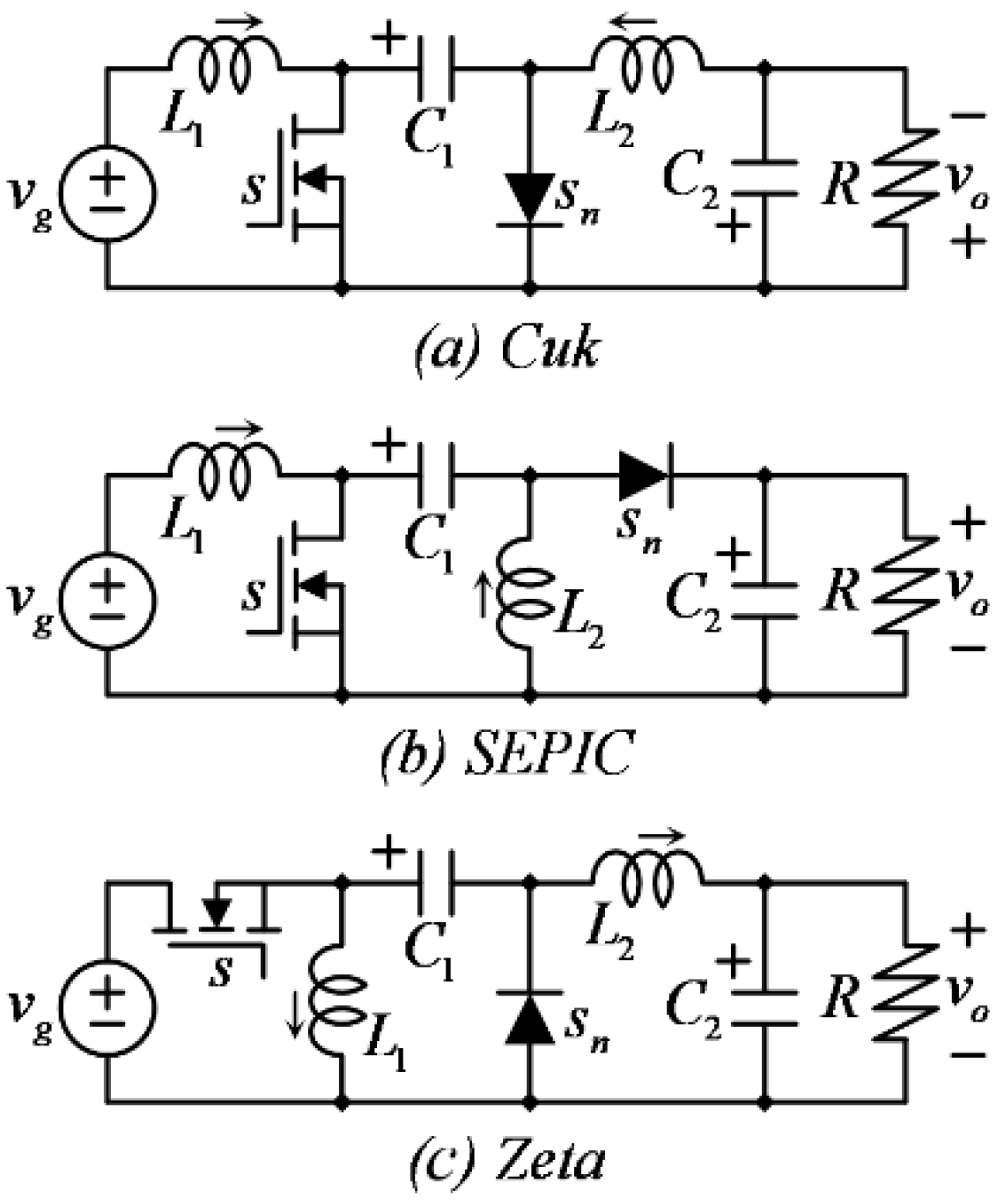
Electronics 10 02379 g001
Figure 2. Fourth order (FO) converters: (a) Cuk, (b) SEPIC, and (c) Zeta converters.
Electronics 10 02379 g002
Figure 3. Fourth order version of the basic family of converters: (a) FO-buck, (b) FO-buck-boost, and (c) FO-boost (super-boost) converters.
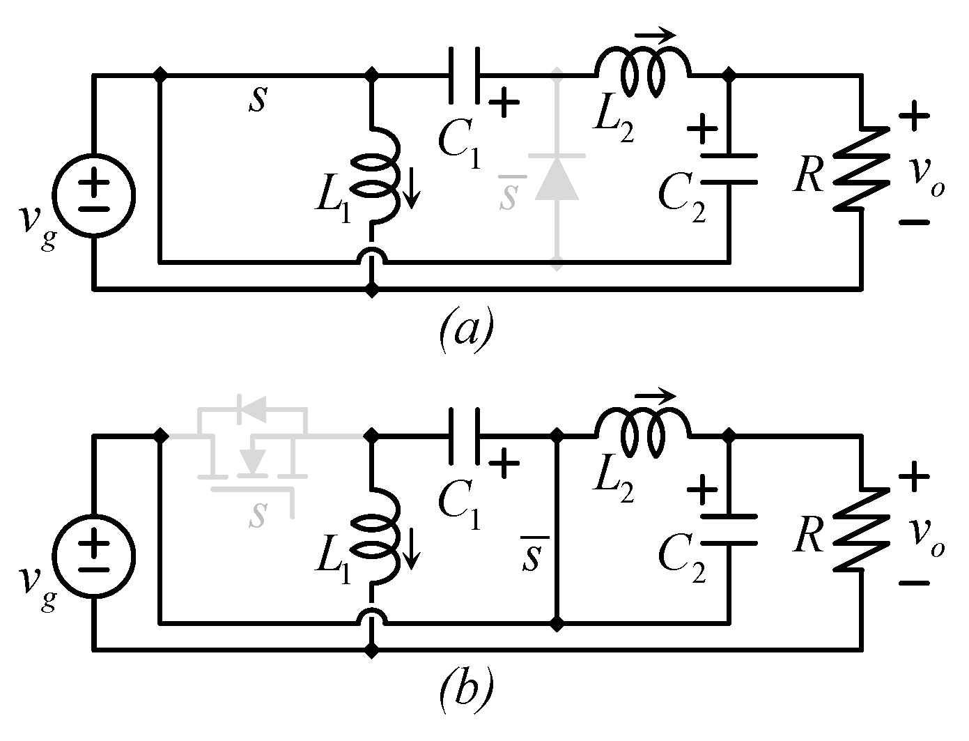
Electronics 10 02379 g003
Figure 4. Equivalent circuits of the super-boost converter according to the switching state (a) when the switch is closed and (b) when the switch is open.
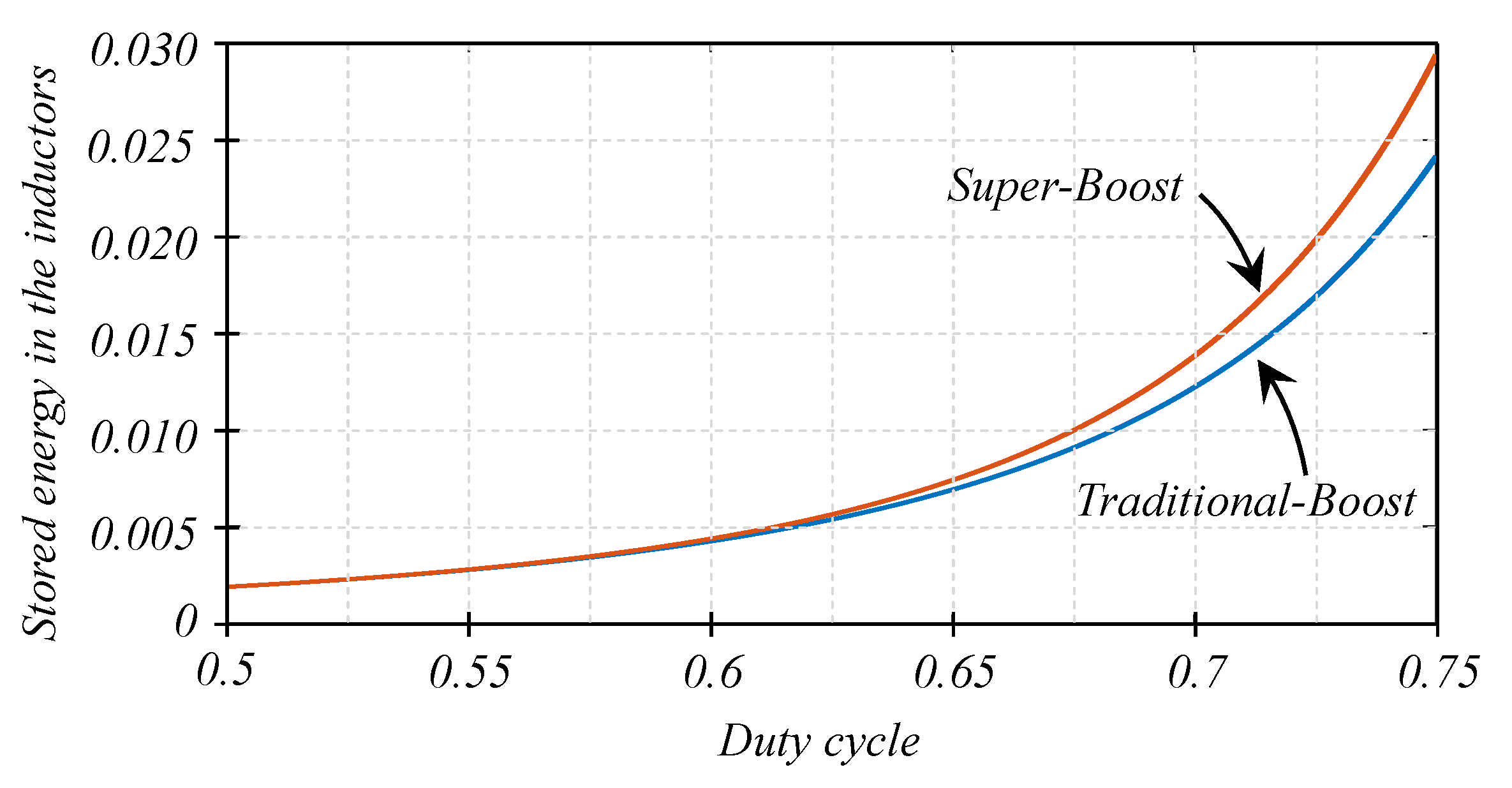
Electronics 10 02379 g004
Figure 5. Comparison of stored energy in inductors between the traditional boost and the super-boost converter for a case with the same input current ripple.
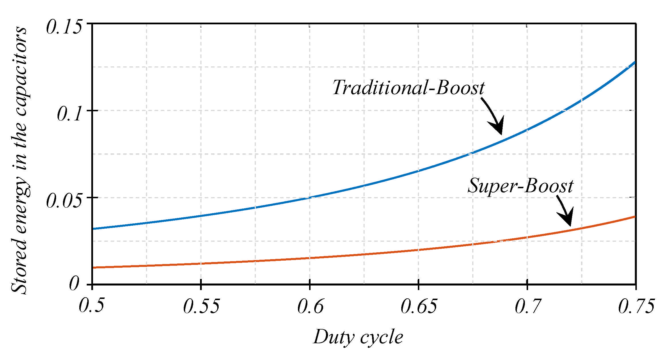
Electronics 10 02379 g005
Figure 6. Comparison of stored energy in capacitors between the traditional boost and the super-boost converter for a case with the same output voltage ripple.
Electronics 10 02379 g006
Figure 7. The proposed improved super-boost ISB converter.
Electronics 10 02379 g007
Figure 8. Equivalent circuits when the transistor is (a) on and (b) off.
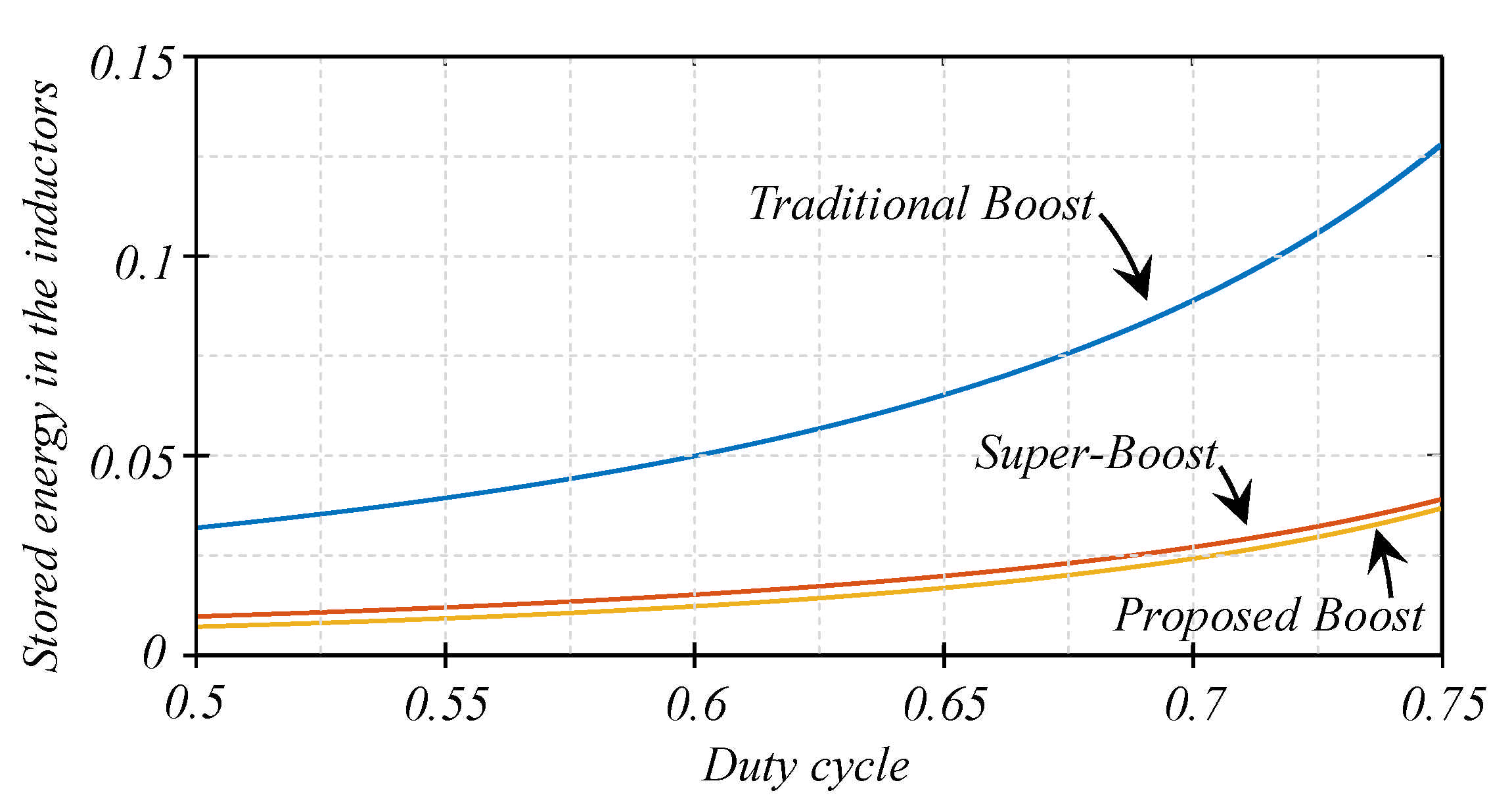
Electronics 10 02379 g008
Figure 9. The stored energy in inductors is compared between the traditional boost, the super boost, and the proposed ISB converter.
Electronics 10 02379 g009
Figure 10. Comparison of stored energy in capacitors between the traditional boost, the super-boost converter, and the proposed converter for a case with the same output voltage ripple.
Electronics 10 02379 g010
Figure 11. Result of the design with the traditional boost converter.
Electronics 10 02379 g011
Figure 12. Result of the design with the super-boost converter.
Electronics 10 02379 g012
Figure 13. Result of the design with the proposed topology.
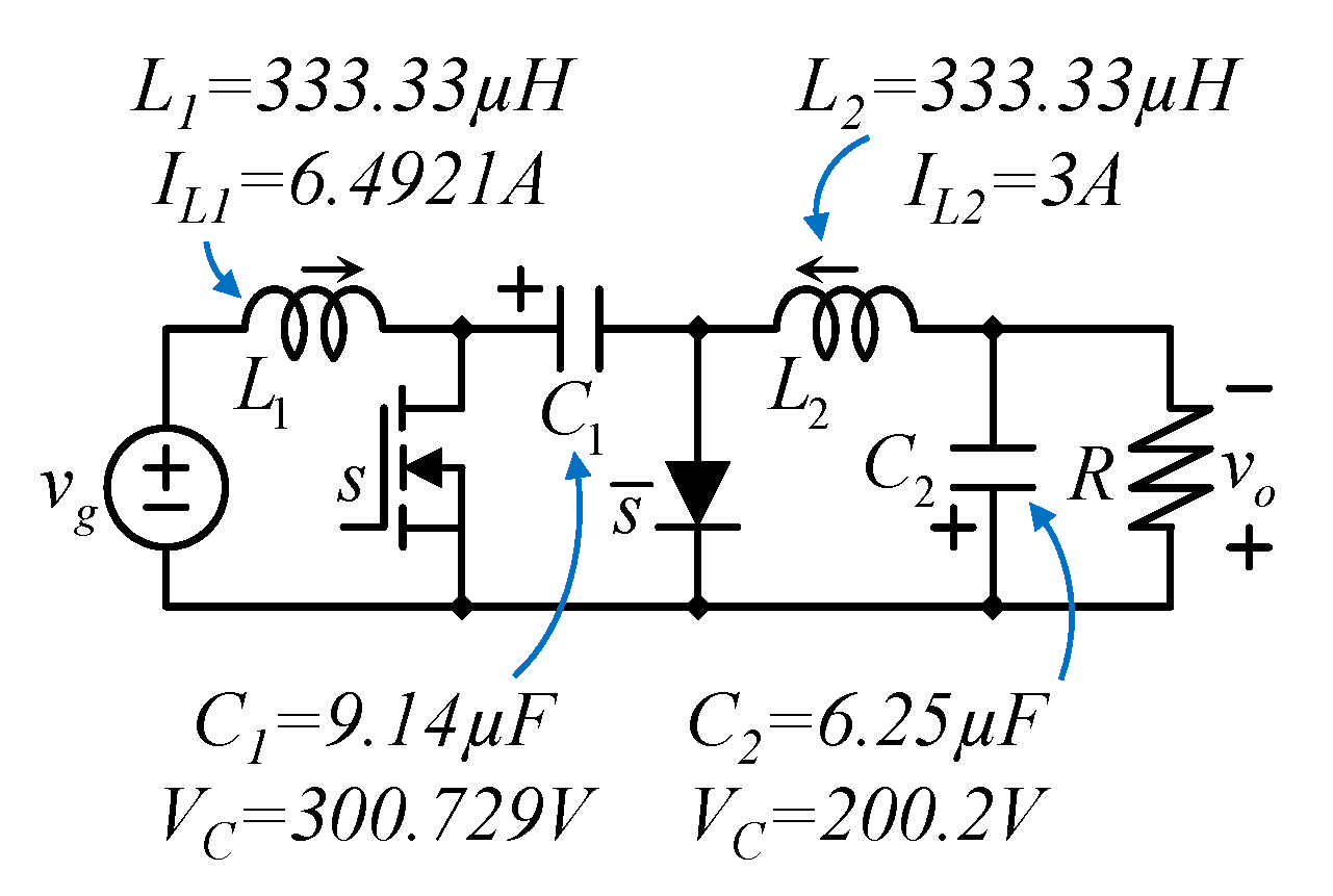
Electronics 10 02379 g013
Figure 14. Result of the design with the Cuk converter topology.
Electronics 10 02379 g014
Figure 15. Result of the design with the SEPIC converter topology.
Electronics 10 02379 g015
Figure 16. Result of the design with the Zeta converter topology.
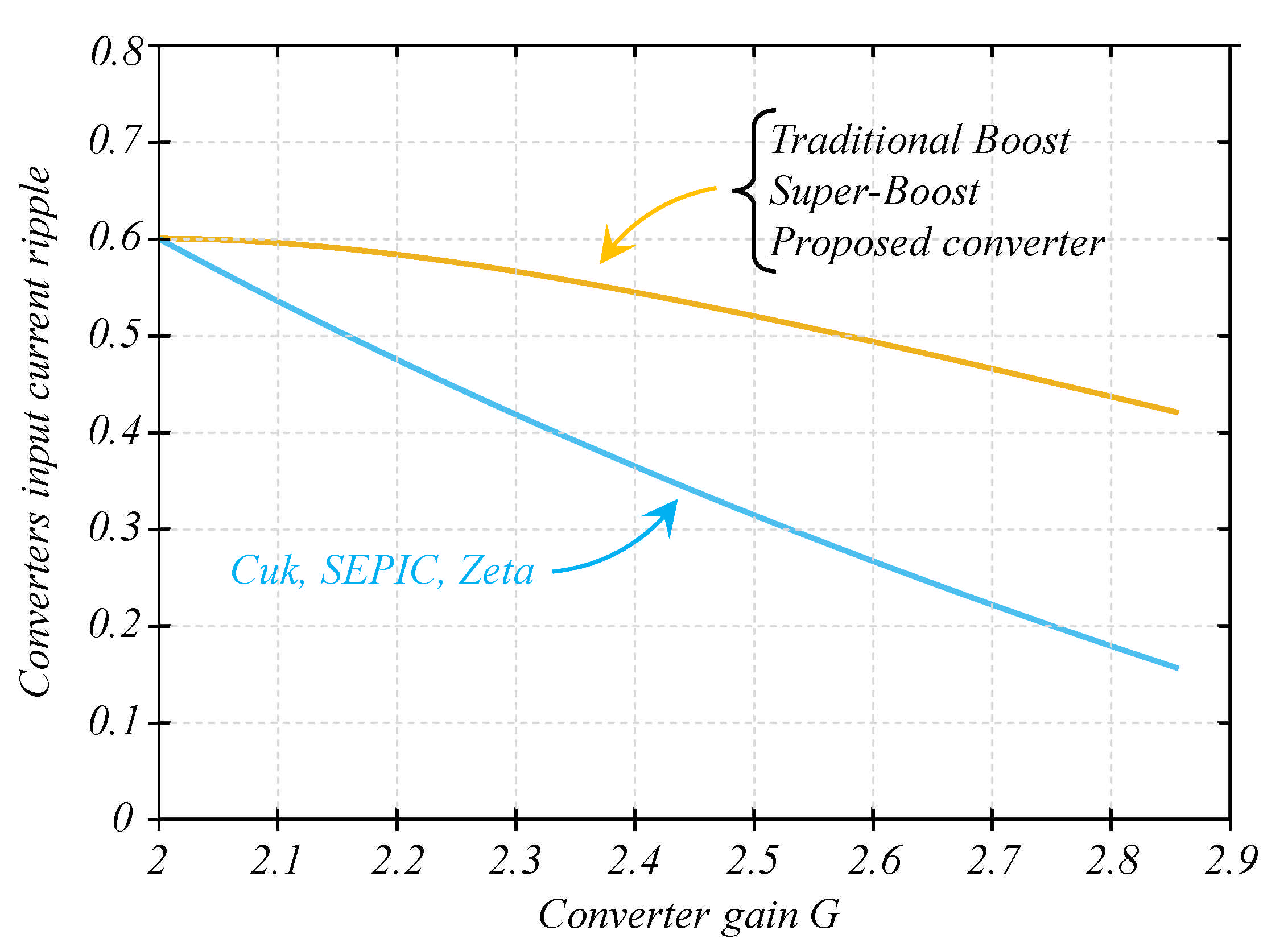
Electronics 10 02379 g016
Figure 17. Input current ripple for all solutions in the full operation range vs. the converter gain G; they were designed to have an input current ripple of 0.6 A in the worst case; for all converters, the worst case is when G = 2.
Electronics 10 02379 g017
Figure 18. Stored energy in inductors for all topologies in the full operation range vs. the converter gain G.
Electronics 10 02379 g018
Figure 19. Output voltage ripple for all solutions in the full operation range vs. the converter gain G; they were designed to have an input current ripple of 0.6 A in the worst case; for all converters, the worst case is when G = 2.
Electronics 10 02379 g019
Figure 20. Stored energy in capacitors for all topologies in the full operation range vs. the converter gain G.
Electronics 10 02379 g020
Figure 21. From button to top: the switching function of the transistor s, current through inductors, and input current when Vg = 70 V, Vo = 200 V, Po = 400 W.
Electronics 10 02379 g021
Figure 22. From button to top: the switching function of the transistor s, current through inductors, and input current when Vg = 85 V, Vo = 200 V, Po = 400 W.
Electronics 10 02379 g022
Figure 23. From button to top: the switching function of the transistor s, current through inductors, and input current when Vg = 100 V, Vo = 200 V, Po = 400 W.
Electronics 10 02379 g023
Figure 24. Switching function “s”, capacitors and output voltage (Vg = 70 V, Vo = 200 V, Po = 400 W).
Electronics 10 02379 g024
Figure 25. Switching function “s”, capacitors and output voltage (Vg = 85 V, Vo = 200 V, Po = 400 W).
Electronics 10 02379 g025
Figure 26. Switching function “s”, capacitors and output voltage (Vg = 100 V, Vo = 200 V, Po = 400 W).
Electronics 10 02379 g026
Figure 27. Closed-loop test, the input voltage Vg changes from 100 V to 70 V and then 100 V again, Vo is regulated to 200 V, Po = 400 W.
Electronics 10 02379 g027
Figure 28. Closed-loop test in which the output power Po changes from 400 W to 80 W, and then it increases back to 400 W again, Vo is regulated to 200 V.
Electronics 10 02379 g028
Figure 29. Closed-loop test, the input voltage Vg changes from 100 V to 85 V and then 100 V again, Vo is regulated to 200 V, Po = 400 W.
Electronics 10 02379 g029
Figure 30. Closed-loop test, the output power Po changes from 400 W to 300 W and then, it increases back to 400 W again, Vo is regulated to 200 V.
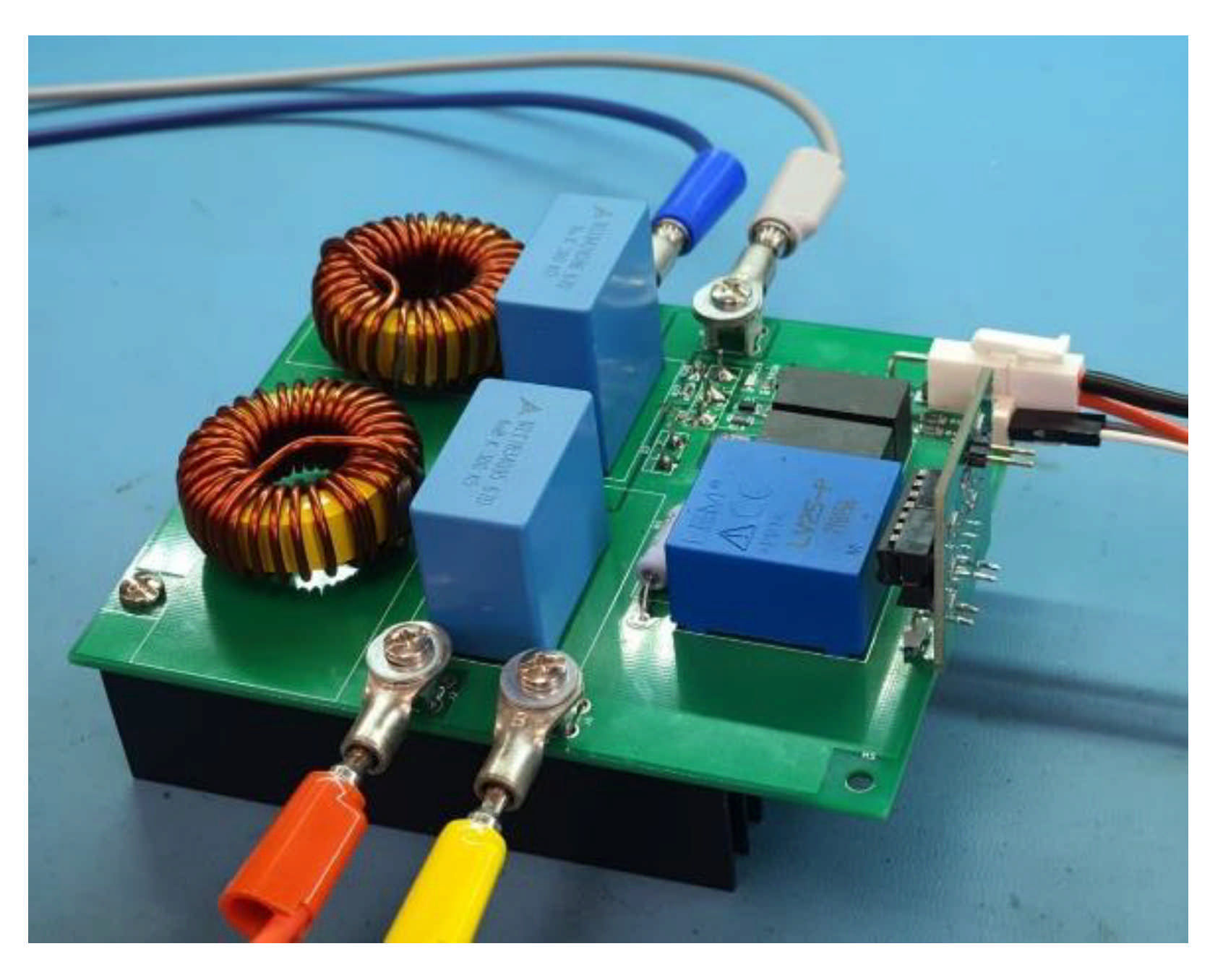
Electronics 10 02379 g030
Figure 31. Prototype photo.
Electronics 10 02379 g031
Table 1. Conventional boost converter design.
Inductor L and Capacitor CL = 250 µH and C = 32.5 µF
Peak current in the inductor6.6243 A
Peak stored energy in the inductor5.5 mJ
Stored energy in the capacitor651.3 mJ
Table 2. Super-boost converter design.
Inductors L1 and L2L1 = 500 µH, L2 = 500 µH
Capacitor C1 and C2C1 = 10.83 µF, C2 = 3.125 µF
Peak current in L14.1693 A
Peak current in L23 A
Peak stored energy in inductors5.9 mJ
Stored energy in both capacitors280.6 mJ
Table 3. Proposed converter results.
Inductor L1 and L2L1 = 250 µH, L2 = 250 µH
Capacitor C1 and C2C1 = 10.83 µF, C2 = 6.25 µF
Peak current in inductor L14.6243 A
Peak current in inductor L23 A
Peak stored energy in inductors3.7 mJ
Stored energy in capacitors270.9 mJ
Table 4. Cuk converter results.
Inductor L1 and L2L1 = 333.33 µH, L2 = 333.33 µH
Capacitor C1 and C2C1 = 9.14 µF, C2 = 6.25 µF
Peak current in inductor L16.4921 A
Peak current in inductor L23 A
Peak stored energy in inductors8.3 mJ
Stored energy in capacitors538.8 mJ
Table 5. SEPIC converter results.
Inductor L1 and L2L1 = 333.33 µH, L2 = 333.33 µH
Capacitor C1 and C2C1 = 35.27 µF, C2 = 37.03 µF
Peak current in inductor L16.4921 A
Peak current in inductor L23 A
Peak stored energy in inductors8.3 mJ
Stored energy in capacitors919.1 mJ
Table 6. Zeta converter results.
Inductor L1 and L2L1 = 333.33 µH, L2 = 333.33 µH
Capacitor C1 and C2C1 = 12.34 µF, C2 = 6.25 µF
Peak current in inductor L16.4921 A
Peak current in inductor L23 A
Peak stored energy in inductors8.3 mJ
Stored energy in capacitors373.6 mJ
Publisher’s Note: MDPI stays neutral with regard to jurisdictional claims in published maps and institutional affiliations.

