
Design and Assessment of Hybrid MTJ/CMOS Circuits for In-Memory-Computation

Abstract
:1. Introduction
2. Background
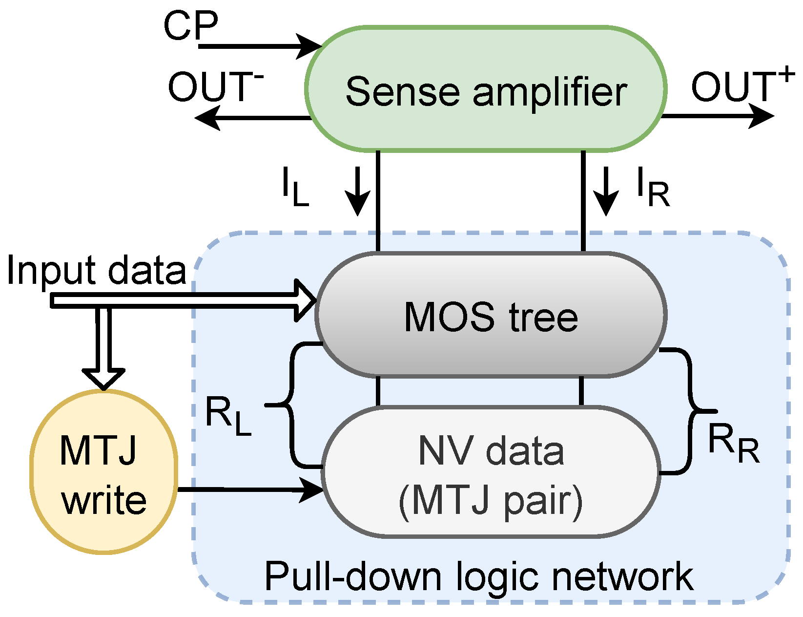
2.1. In-Memory-Computation Architecture
2.2. Spin Transfer Torque Write Circuit
2.3. Spin-Hall Effect Assisted Spin Transfer Torque Write Circuit
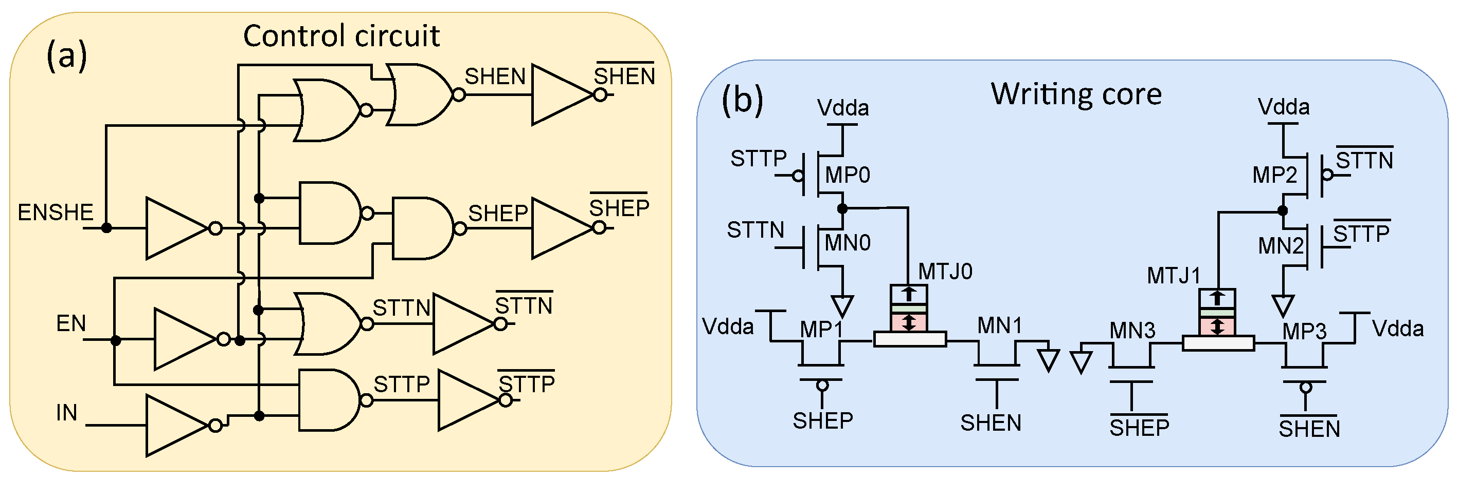
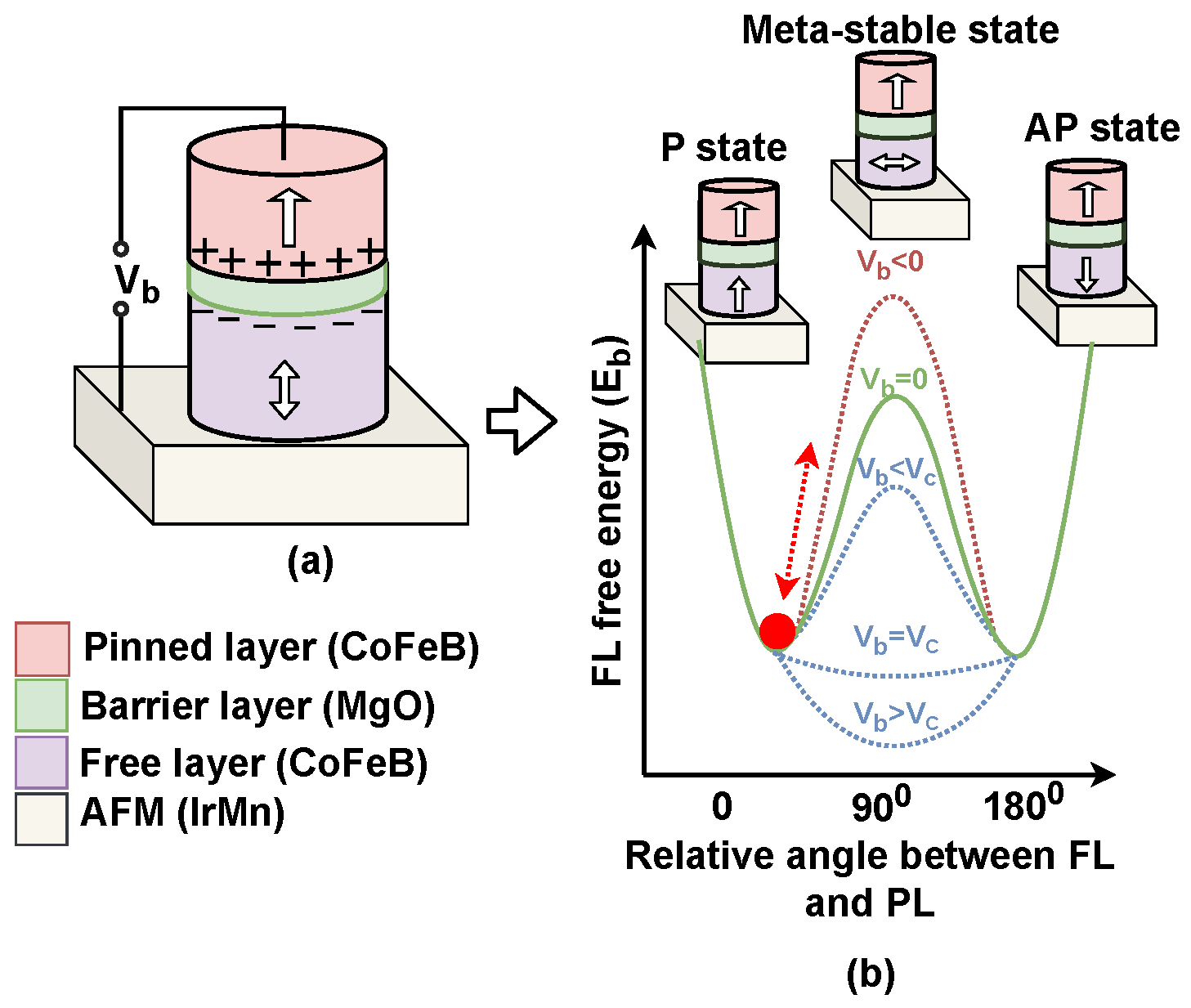
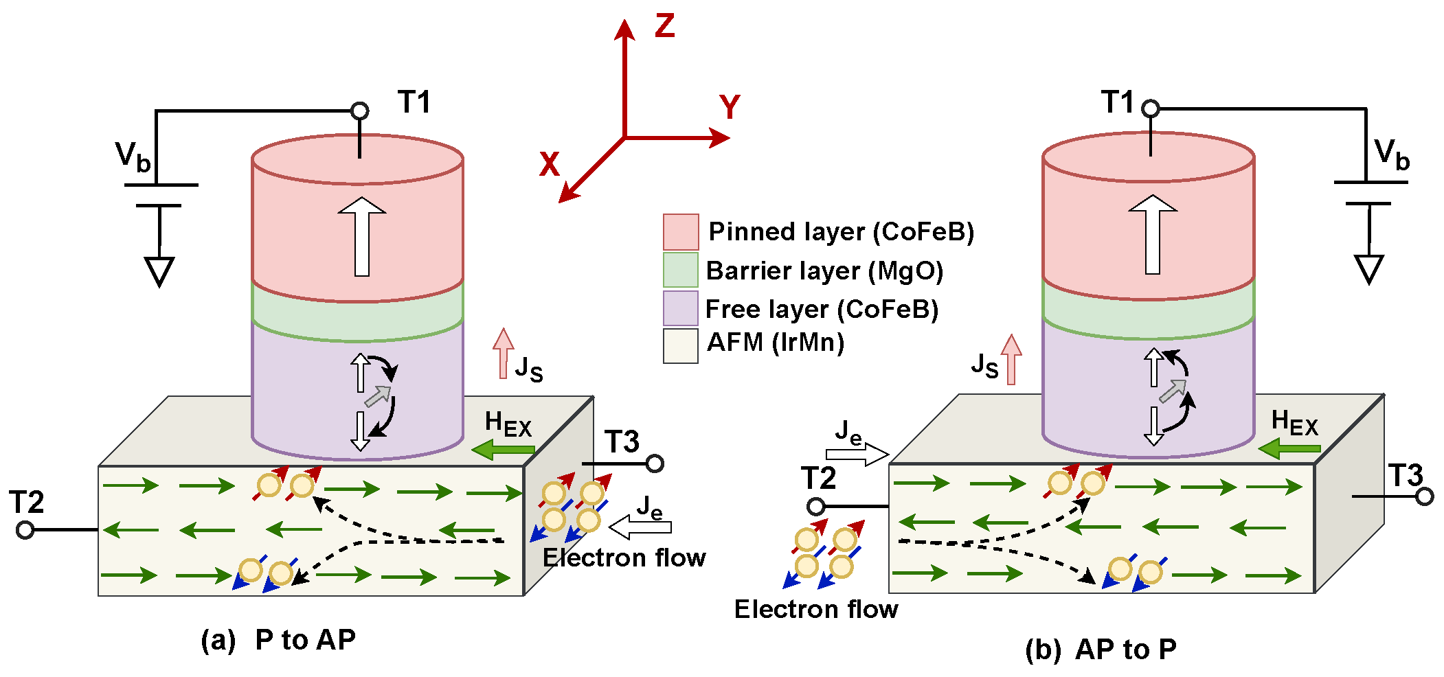
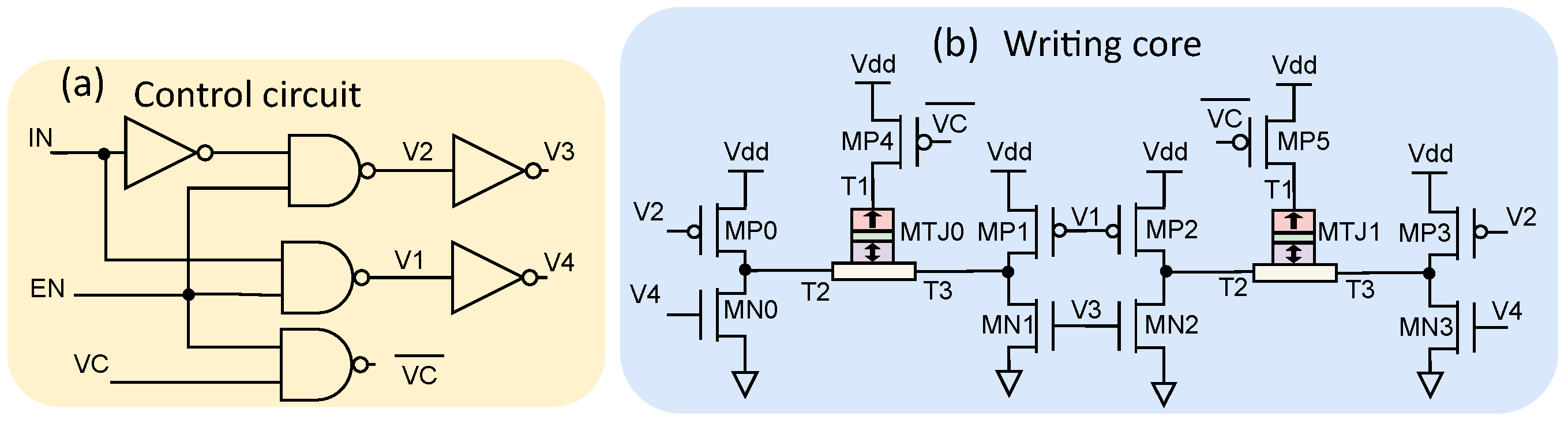
3. Voltage Gated Spin Orbit Torque: Mechanism and Novel Write Circuit
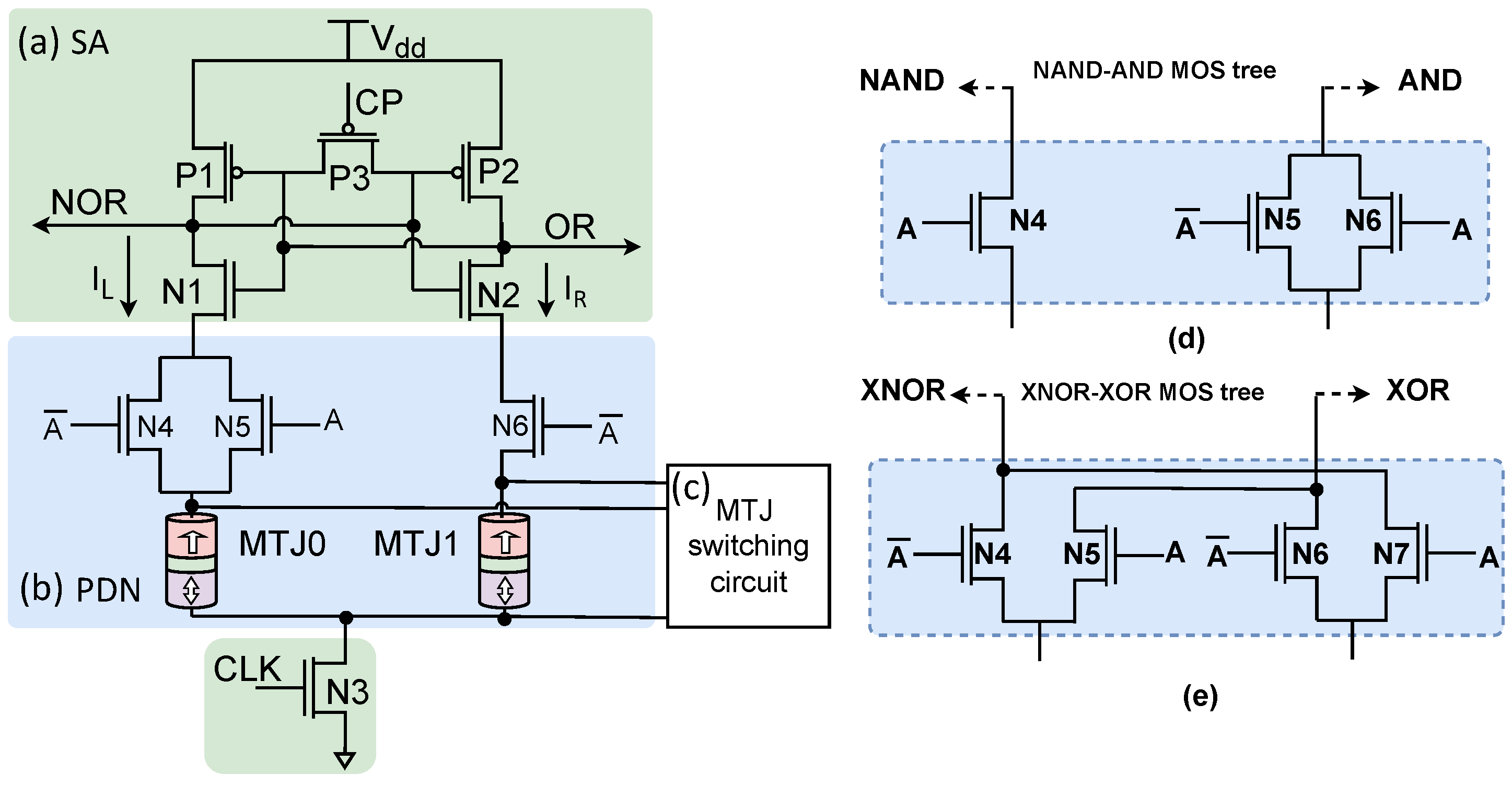
4. Logic Gates Based on IMC
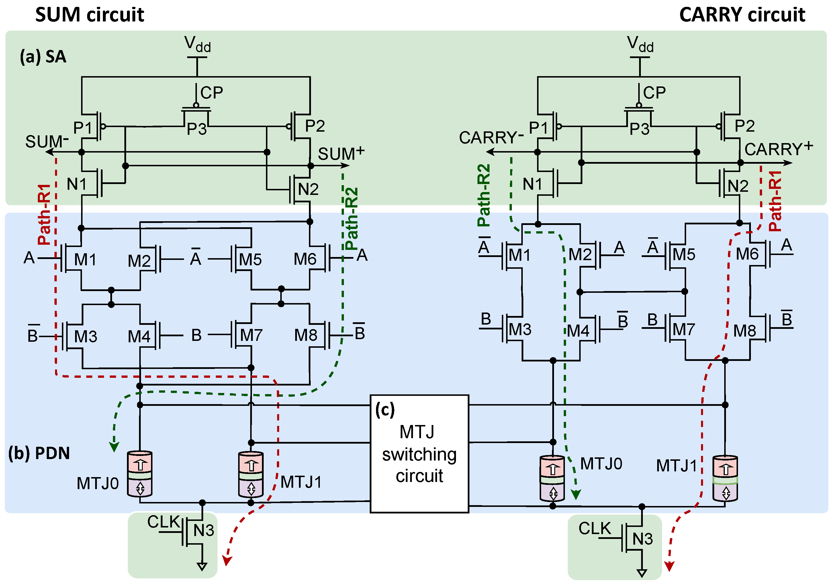
5. IMC Based Full Adder
6. Simulation Results and Discussion
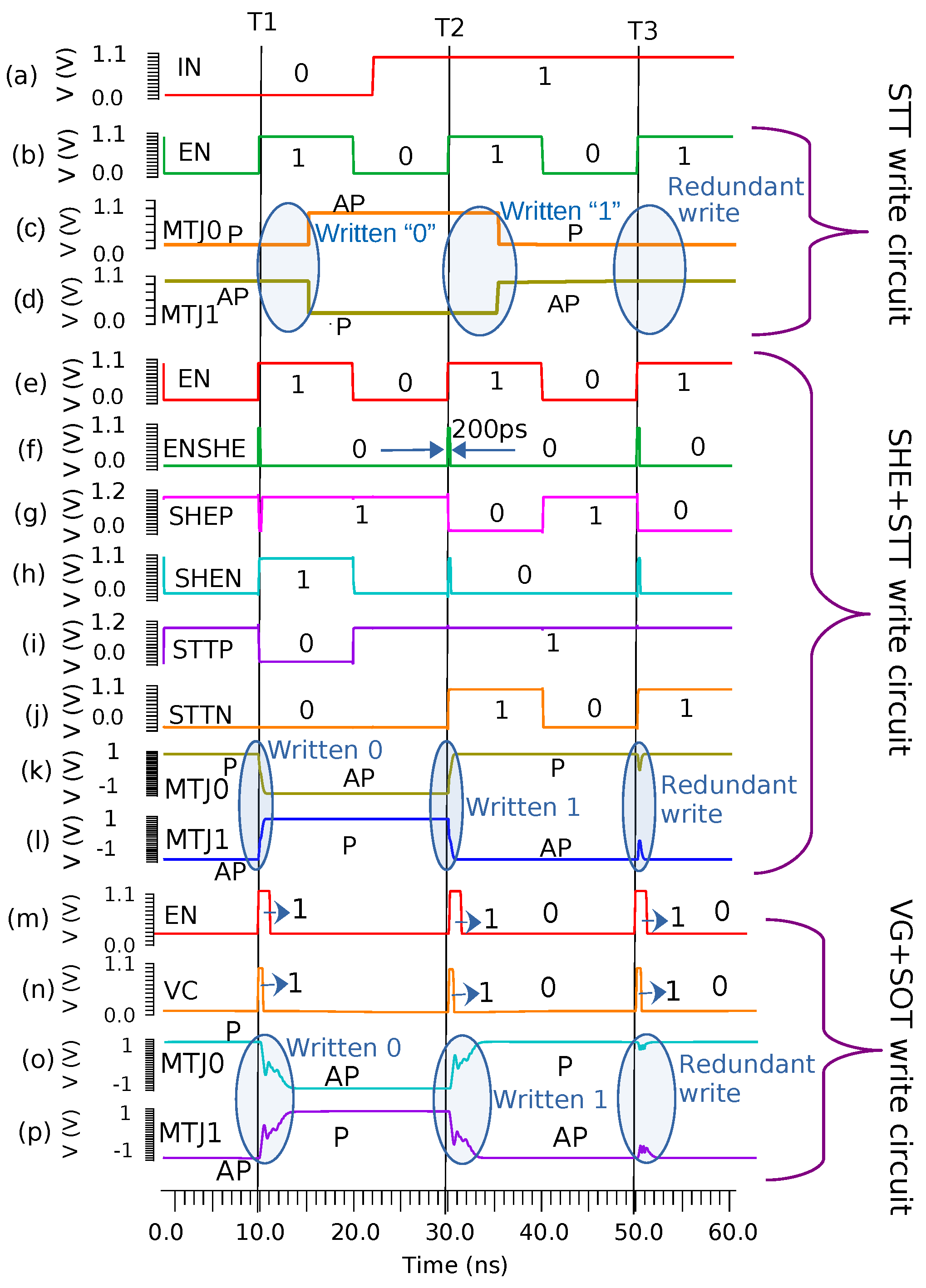
6.1. Write Circuits
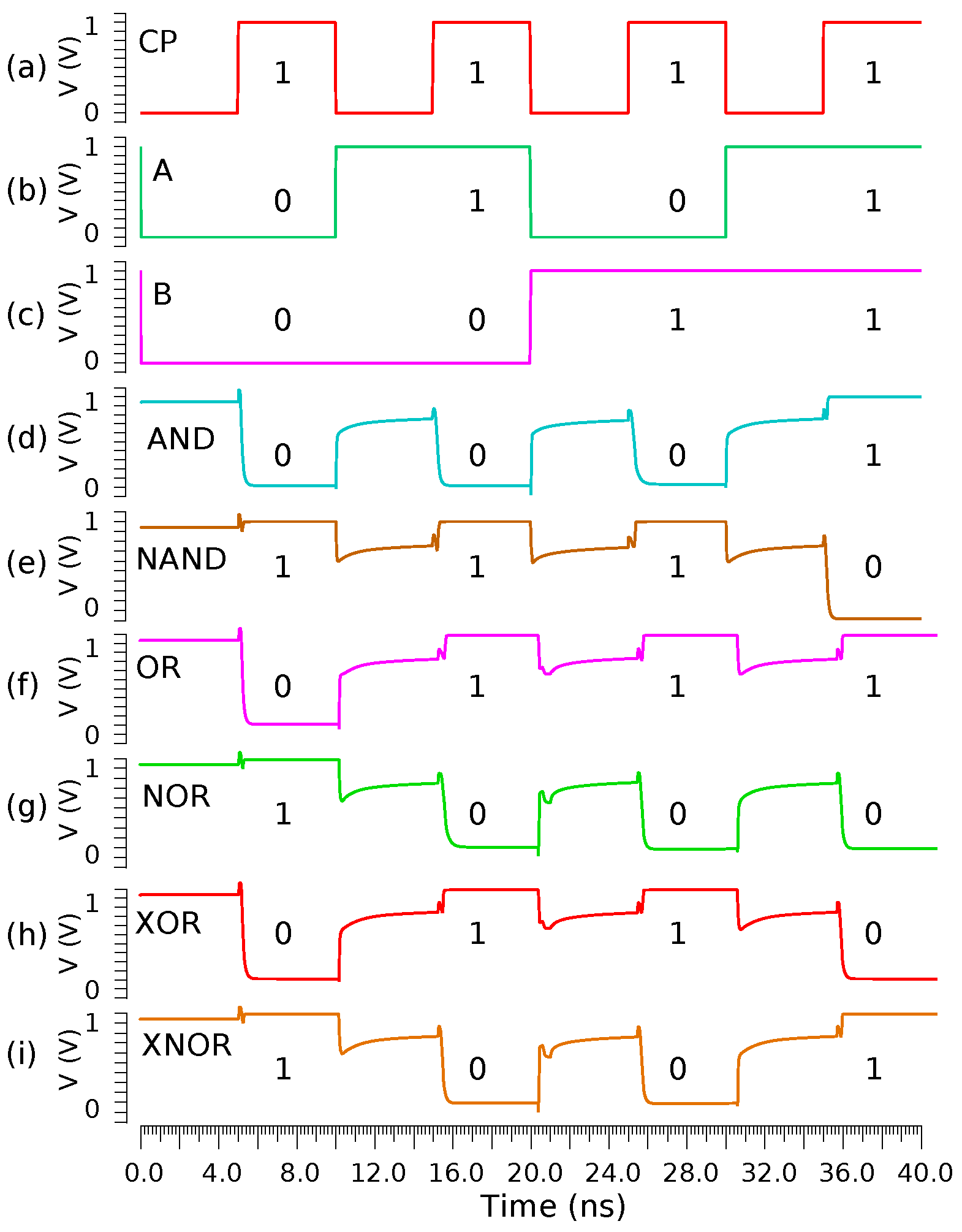
6.2. Performance of Logic Gates
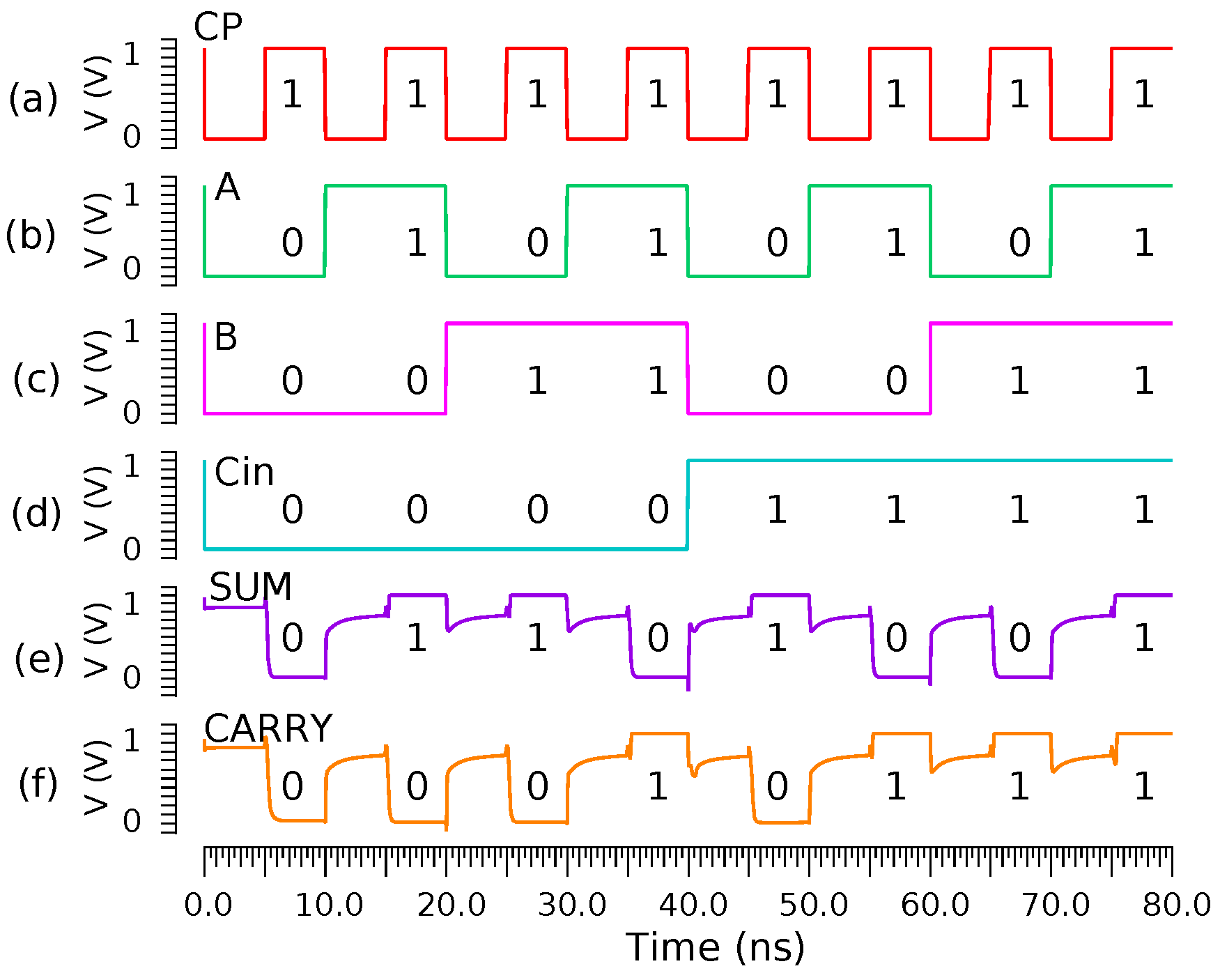
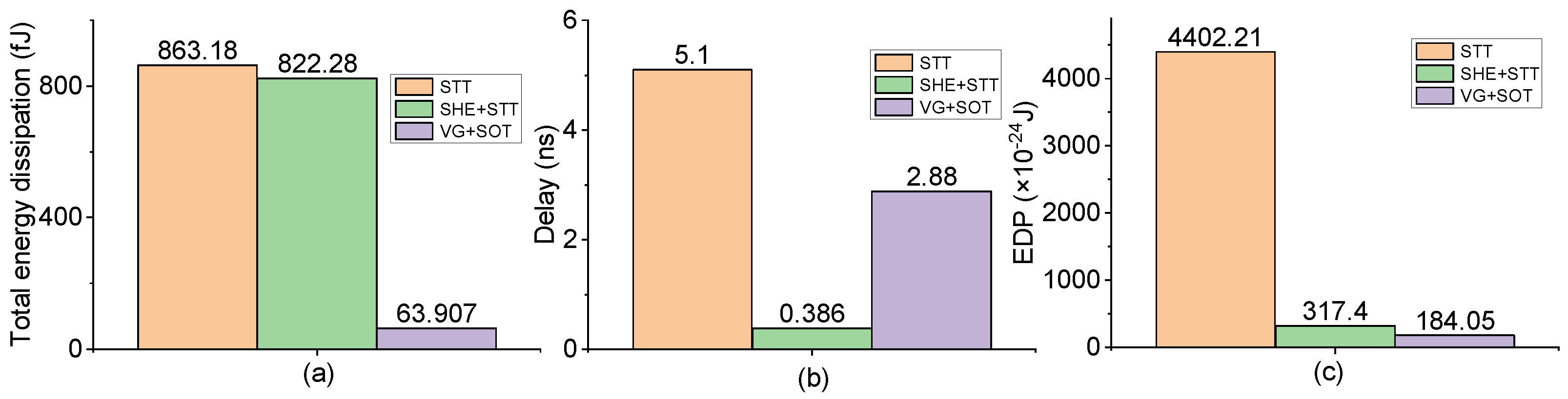
6.3. Performance of NV-FA Circuits
7. Conclusions
Author Contributions
Funding
Data Availability Statement
Conflicts of Interest
Abbreviations
| P | Parallel |
| AP | Antiparallel |
| PL | Pinned layer |
| FL | Fixed layer |
| BL | Barrier layer |
| IMC | In-memory-computation |
| MTJ | Magnetic tunnel junction |
| p-MTJ | Perpendicular magnetic tunnel junction |
| STT | Spin transfer torque |
| MRAM | Magnetoresistance random access memory |
| SRAM | Static random access memory |
| SHE+STT | Spin-Hall effected assisted Spin transfer torque |
| VCMA | Voltage controlled magnetic anisotropy |
| VG+SOT | Voltage-gated spin orbit torque |
| SOI | Spin–orbit interaction |
| SOC | Spin orbit coupling |
| HM | Heavy metal |
| AFM | Antiferromagnetic material |
| LLG | Landau–Lifshitz–Gilbert |
References
- Haensch, W.; Raghunathan, A.; Roy, K.; Chakrabarti, B.; Phatak, C.M.; Wang, C.; Guha, S. Compute in-Memory with Non-Volatile Elements for Neural Networks: A Review from a Co-Design Perspective. Adv. Mater. 2023, 35, 2204944. [Google Scholar] [CrossRef] [PubMed]
- Seo, J.s.; Saikia, J.; Meng, J.; He, W.; Suh, H.S.; Anupreetham; Liao, Y.; Hasssan, A.; Yeo, I. Digital Versus Analog Artificial Intelligence Accelerators: Advances, trends, and emerging designs. IEEE Solid-State Circuits Mag. 2022, 14, 65–79. [Google Scholar] [CrossRef]
- LeCun, Y.; Bengio, Y.; Hinton, G. Deep learning. Nature 2015, 521, 436–444. [Google Scholar] [CrossRef] [PubMed]
- Burr, G.W.; Lim, S.; Murmann, B.; Venkatesan, R.; Verhelst, M. Fair and Comprehensive Benchmarking of Machine Learning Processing Chips. IEEE Des. Test 2021, 39, 18–27. [Google Scholar] [CrossRef]
- Ielmini, D.; Wong, H.S.P. In-memory computing with resistive switching devices. Nat. Electron. 2018, 1, 333–343. [Google Scholar] [CrossRef]
- Zhao, W.; Prenat, G. (Eds.) Spintronics-Based Computing; Springer International Publishing: Cham, Switzerland, 2015. [Google Scholar]
- Collaert, N. Advancements in IC Technologies: A look toward the future. IEEE Solid-State Circuits Mag. 2023, 15, 80–86. [Google Scholar] [CrossRef]
- Yu, S.; Jiang, H.; Huang, S.; Peng, X.; Lu, A. Compute-in-Memory Chips for Deep Learning: Recent Trends and Prospects. IEEE Circuits Syst. Mag. 2021, 21, 31–56. [Google Scholar] [CrossRef]
- Sebastian, A.; Le Gallo, M.; Khaddam-Aljameh, R.; Eleftheriou, E. Memory devices and applications for in-memory computing. Nat. Nanotechnol. 2020, 15, 529–544. [Google Scholar] [CrossRef]
- Verma, N.; Jia, H.; Valavi, H.; Tang, Y.; Ozatay, M.; Chen, L.Y.; Zhang, B.; Deaville, P. In-Memory Computing: Advances and Prospects. IEEE Solid-State Circuits Mag. 2019, 11, 43–55. [Google Scholar] [CrossRef]
- Dong, Q.; Sinangil, M.E.; Erbagci, B.; Sun, D.; Khwa, W.S.; Liao, H.J.; Wang, Y.; Chang, J. 15.3 A 351TOPS/W and 372.4GOPS Compute-in-Memory SRAM Macro in 7 nm FinFET CMOS for Machine-Learning Applications. In Proceedings of the 2020 IEEE International Solid-State Circuits Conference—(ISSCC), San Francisco, CA, USA, 16–20 February 2020; pp. 16–20. [Google Scholar] [CrossRef]
- Jiang, Z.; Yin, S.; Seo, J.S.; Seok, M. C3SRAM: An In-Memory-Computing SRAM Macro Based on Robust Capacitive Coupling Computing Mechanism. IEEE J. Solid-State Circuits 2020, 55, 1888–1897. [Google Scholar] [CrossRef]
- Zhang, J.; Wang, Z.; Verma, N. In-Memory Computation of a Machine-Learning Classifier in a Standard 6T SRAM Array. IEEE J. Solid-State Circuits 2017, 52, 915–924. [Google Scholar] [CrossRef]
- Gonugondla, S.K.; Kang, M.; Shanbhag, N. A 42pJ/decision 3.12TOPS/W robust in-memory machine learning classifier with on-chip training. In Proceedings of the 2018 IEEE International Solid - State Circuits Conference—(ISSCC), San Francisco, CA, USA, 11–15 February 2018; pp. 11–15. [Google Scholar] [CrossRef]
- Rajput, P.J.; Bhandari, S.U.; Wadhwa, G. A Review on—Spintronics an Emerging Technology. Silicon 2022, 14, 9195–9210. [Google Scholar] [CrossRef]
- Qin, J.; Sun, B.; Zhou, G.; Guo, T.; Chen, Y.; Ke, C.; Mao, S.; Chen, X.; Shao, J.; Zhao, Y. From Spintronic Memristors to Quantum Computing. ACS Mater. Lett. 2023, 5, 2197–2215. [Google Scholar] [CrossRef]
- Kang, W.; Deng, E.; Wang, Z.; Zhao, W. Spintronic Logic-in-Memory Paradigms and Implementations. Appl. Emerg. Mem. Technol. 2020, 63, 215–229. [Google Scholar]
- Yu, S.; Chen, P.Y. Emerging Memory Technologies: Recent Trends and Prospects. IEEE Solid-State Circuits Mag. 2016, 8, 43–56. [Google Scholar] [CrossRef]
- Finocchio, G.; Di Ventra, M.; Camsari, K.Y.; Everschor-Sitte, K.; Khalili Amiri, P.; Zeng, Z. The promise of spintronics for unconventional computing. J. Magn. Magn. Mater. 2021, 521, 167506. [Google Scholar] [CrossRef]
- Ikeda, S.; Hayakawa, J.; Ashizawa, Y.; Lee, Y.M.; Miura, K.; Hasegawa, H.; Tsunoda, M.; Matsukura, F.; Ohno, H. Tunnel magnetoresistance of 604% at 300K by suppression of Ta diffusion in CoFeB/MgO/CoFeB pseudo-spin-valves annealed at high temperature. Appl. Phys. Lett. 2008, 93, 082508–1–082508–3. [Google Scholar] [CrossRef]
- Spin-Transfer Torque DDR Products|Everspin. 2023. Available online: https://www.everspin.com/spin-transfer-torque-ddr-products (accessed on 17 July 2023).
- Golonzka, O.; Alzate, J.G.; Arslan, U.; Bohr, M.; Bai, P.; Brockman, J.; Buford, B.; Connor, C.; Das, N.; Doyle, B.; et al. MRAM as Embedded Non-Volatile Memory Solution for 22FFL FinFET Technology. In Proceedings of the 2018 IEEE International Electron Devices Meeting (IEDM), San Francisco, CA, USA, 1–5 December 2018; pp. 1–5. [Google Scholar] [CrossRef]
- van den Brink, A.; Cosemans, S.; Cornelissen, S.; Manfrini, M.; Vaysset, A.; Van Roy, W.; Min, T.; Swagten, H.J.M.; Koopmans, B. Spin-Hall-assisted magnetic random access memory. Appl. Phys. Lett. 2014, 104, 012403. [Google Scholar] [CrossRef]
- Lin, X.; Zhu, L. Magnetization switching in van der Waals systems by spin-orbit torque. Mater. Today Electron. 2023, 4, 100037. [Google Scholar] [CrossRef]
- Deng, J.; Liang, G.; Gupta, G. Ultrafast and low-energy switching in voltage-controlled elliptical pMTJ. Sci. Rep. 2017, 7, 1–10. [Google Scholar] [CrossRef]
- Sarwat, S.G. Materials science and engineering of phase change random access memory. Mater. Sci. Technol. 2017, 33, 1890–1906. [Google Scholar] [CrossRef]
- Long, M.; Zeng, L.; Gao, T.; Zhang, D.; Qin, X.; Zhang, Y.; Zhao, W. Self-Adaptive Write Circuit for Magnetic Tunneling Junction Memory With Voltage-Controlled Magnetic Anisotropy Effect. IEEE Trans. Nanotechnol. 2018, 17, 492–499. [Google Scholar] [CrossRef]
- Yoshida, C.; Tanaka, T.; Ataka, T.; Hoshina, M.; Furuya, A. Field-free reliable magnetization switching in a three-terminal perpendicular magnetic tunnel junction via spin-orbit torque, spin-transfer torque, and voltage-controlled magnetic anisotropy. J. Phys. D Appl. Phys. 2022, 55, 365003. [Google Scholar] [CrossRef]
- Wu, H.; Zhang, J.; Cui, B.; Razavi, S.A.; Che, X.; Pan, Q.; Wu, D.; Yu, G.; Han, X.; Wang, K.L. Field-free approaches for deterministic spin–orbit torque switching of the perpendicular magnet. Mater. Futures 2022, 1, 022201. [Google Scholar] [CrossRef]
- Zhang, K.; Zhang, D.; Wang, C.; Zeng, L.; Wang, Y.; Zhao, W. Compact Modeling and Analysis of Voltage-Gated Spin-Orbit Torque Magnetic Tunnel Junction. IEEE Access 2020, 8, 50792–50800. [Google Scholar] [CrossRef]
- Wu, Y.C.; Garello, K.; Kim, W.; Gupta, M.; Perumkunnil, M.; Kateel, V.; Couet, S.; Carpenter, R.; Rao, S.; Van Beek, S.; et al. Voltage-Gate-Assisted Spin-Orbit-Torque Magnetic Random-Access Memory for High-Density and Low-Power Embedded Applications. Phys. Rev. Appl. 2021, 15, 064015. [Google Scholar] [CrossRef]
- Wang, C.; Zhang, D.; Zhang, K.; Zeng, L.; Wang, Y.; Hou, Z.; Zhang, Y.; Zhao, W. Magnetic Nonvolatile SRAM Based on Voltage-Gated Spin-Orbit-Torque Magnetic Tunnel Junctions. IEEE Trans. Electron Devices 2020, 67, 1965–1971. [Google Scholar] [CrossRef]
- Dieny, B.; Chshiev, M. Perpendicular magnetic anisotropy at transition metal/oxide interfaces and applications. Rev. Mod. Phys. 2017, 89, 025008. [Google Scholar] [CrossRef]
- Shao, Q.; Li, P.; Liu, L.; Yang, H.; Fukami, S.; Razavi, A.; Wu, H.; Wang, K.; Freimuth, F.; Mokrousov, Y.; et al. Roadmap of spin-orbit torques. IEEE Trans. Magn. 2021, 57, 800439. [Google Scholar] [CrossRef]
- Wang, Z.; Zhao, W.; Deng, E.; Zhang, Y.; Klein, J.O. Magnetic non-volatile flip-flop with spin-Hall assistance. Phys. Status Solidi RRL 2015, 9, 375–378. [Google Scholar] [CrossRef]
- Lee, H.; Lee, A.; Wang, S.; Ebrahimi, F.; Gupta, P.; Amiri, P.K.; Wang, K.L. Analysis and Compact Modeling of Magnetic Tunnel Junctions Utilizing Voltage-Controlled Magnetic Anisotropy. IEEE Trans. Magn. 2018, 54, 4400209. [Google Scholar] [CrossRef]
- Grezes, C.; Ebrahimi, F.; Alzate, J.G.; Cai, X.; Katine, J.A.; Langer, J.; Ocker, B.; Khalili Amiri, P.; Wang, K.L. Ultra-low switching energy and scaling in electric-field-controlled nanoscale magnetic tunnel junctions with high resistance-area product. Appl. Phys. Lett. 2016, 108, 012403. [Google Scholar] [CrossRef]
- Miura, K.; Yabuuchi, S.; Yamada, M.; Ichimura, M.; Rana, B.; Ogawa, S.; Takahashi, H.; Fukuma, Y.; Otani, Y. Voltage-induced magnetization dynamics in CoFeB/MgO/CoFeB magnetic tunnel junctions. Sci. Rep. 2017, 7, 42511. [Google Scholar] [CrossRef] [PubMed]
- Song, J.; Ahmed, I.; Zhao, Z.; Zhang, D.; Sapatnekar, S.S.; Wang, J.P.; Kim, C.H. Evaluation of Operating Margin and Switching Probability of Voltage- Controlled Magnetic Anisotropy Magnetic Tunnel Junctions. IEEE J. Explor. Solid-State Comput. Devices Circuits 2018, 4, 76–84. [Google Scholar] [CrossRef]
- Song, C.; Cui, B.; Li, F.; Zhou, X.; Pan, F. Recent progress in voltage control of magnetism: Materials, mechanisms, and performance. Prog. Mater. Sci. 2017, 87, 33–82. [Google Scholar] [CrossRef]
- Kang, W.; Ran, Y.; Zhang, Y.; Lv, W.; Zhao, W. Modeling and Exploration of the Voltage-Controlled Magnetic Anisotropy Effect for the Next-Generation Low-Power and High-Speed MRAM Applications. IEEE Trans. Nanotechnol. 2017, 16, 387–395. [Google Scholar] [CrossRef]
- Kang, W.; Ran, Y.; Lv, W.; Zhang, Y.; Zhao, W. High-Speed, Low-Power, Magnetic Non-Volatile Flip-Flop With Voltage-Controlled, Magnetic Anisotropy Assistance. IEEE Magn. Lett. 2016, 7, 1–5. [Google Scholar] [CrossRef]
- Zarei, A.; Safaei, F. Power and area-efficient design of VCMA-MRAM based full-adder using approximate computing for IoT applications. Microelectron. J. 2018, 82, 62–70. [Google Scholar] [CrossRef]
- Zarei, A.; Safaei, F. LIMITA: Logic-in-Memory Primitives for Imprecise Tolerant Applications. IEEE Trans. Circ. Syst. I 2021, 68, 4686–4699. [Google Scholar] [CrossRef]
- Lau, Y.C.; Betto, D.; Rode, K.; Coey, J.M.D.; Stamenov, P. Spin–orbit torque switching without an external field using interlayer exchange coupling. Nat. Nanotechnol. 2016, 11, 758–762. [Google Scholar] [CrossRef]
- Fukami, S.; Zhang, C.; DuttaGupta, S.; Kurenkov, A.; Ohno, H. Magnetization switching by spin–orbit torque in an antiferromagnet–ferromagnet bilayer system. Nat. Mater. 2016, 15, 535–541. [Google Scholar] [CrossRef] [PubMed]
- Qian, L.; Chen, W.; Wang, K.; Wu, X.; Xiao, G. Spin Hall effect and current induced magnetic switching in antiferromagnetic IrMn. AIP Adv. 2018, 8, 115323. [Google Scholar] [CrossRef]
- Manchon, A.; Železný, J.; Miron, I.M.; Jungwirth, T.; Sinova, J.; Thiaville, A.; Garello, K.; Gambardella, P. Current-induced spin-orbit torques in ferromagnetic and antiferromagnetic systems. Rev. Mod. Phys. 2019, 91, 035004. [Google Scholar] [CrossRef]
- Hirohata, A.; Yamada, K.; Nakatani, Y.; Prejbeanu, I.L.; Diény, B.; Pirro, P.; Hillebrands, B. Review on spintronics: Principles and device applications. J. Magn. Magn. Mater. 2020, 509, 166711. [Google Scholar] [CrossRef]
- Jenkins, S.; Chantrell, R.W.; Evans, R.F.L. Exchange bias in multigranular noncollinear IrMn3/CoFe thin films. Phys. Rev. B 2021, 103, 014424. [Google Scholar] [CrossRef]
- Alla, S.; Kumar Joshi, V.; Bhat, S. Field-free switching of VG-SOT-pMTJ device through the interplay of SOT, exchange bias, and VCMA effects. J. Appl. Phys. 2023, 134, 013901. [Google Scholar] [CrossRef]
- Thapliyal, H.; Sharifi, F.; Kumar, S.D. Energy-Efficient Design of Hybrid MTJ/CMOS and MTJ/Nanoelectronics Circuits. IEEE Trans. Magn. 2018, 54, 1–8. [Google Scholar] [CrossRef]
- Zhao, W.; Chappert, C.; Javerliac, V.; Noziere, J.P. High Speed, High Stability and Low Power Sensing Amplifier for MTJ/CMOS Hybrid Logic Circuits. IEEE Trans. Magn. 2009, 45, 3784–3787. [Google Scholar] [CrossRef]
- Cai, K.; Zhu, Z.; Lee, J.M.; Mishra, R.; Ren, L.; Pollard, S.D.; He, P.; Liang, G.; Teo, K.L.; Yang, H. Ultrafast and energy-efficient spin–orbit torque switching in compensated ferrimagnets. Nat. Electron. 2020, 3, 37–42. [Google Scholar] [CrossRef]
- Jeong, J.; Ferrante, Y.; Faleev, S.V.; Samant, M.G.; Felser, C.; Parkin, S.S.P. Termination layer compensated tunnelling magnetoresistance in ferrimagnetic Heusler compounds with high perpendicular magnetic anisotropy. Nat. Commun. 2016, 7, 10276. [Google Scholar] [CrossRef]
- Qin, P.; Yan, H.; Wang, X.; Chen, H.; Meng, Z.; Dong, J.; Zhu, M.; Cai, J.; Feng, Z.; Zhou, X.; et al. Room-temperature magnetoresistance in an all-antiferromagnetic tunnel junction. Nature 2023, 613, 485–489. [Google Scholar] [CrossRef] [PubMed]
- Wang, Z.; Zhao, W.; Deng, E.; Klein, J.O.; Chappert, C. Perpendicular-anisotropy magnetic tunnel junction switched by spin-Hall-assisted spin-transfer torque. J. Phys. D Appl. Phys. 2015, 48, 065001. [Google Scholar] [CrossRef]


| Parameter | Description | Value |
|---|---|---|
| TMR(0) | TMR ratio with zero bias | 200% |
| Shape | MTJ Surface shape | circle |
| MTJ Surface length | 32 nm | |
| MTJ Surface width | 32 nm | |
| MTJ Surface radius | 16 nm | |
| AFM width | 50 nm | |
| AFM thickness | 3 nm | |
| AFM length | 60 nm | |
| Free layer thickness | 1.1 nm | |
| MgO barrier thickness | 1.4 nm | |
| RA | Resistance-area product | 650 µ |
| MTJ Switching Technique | STT | SHE+STT | VG+SOT |
|---|---|---|---|
| Writing core Energy/bit (fJ) | 861.9 | 819.4 | 63.07 |
| Control circuit Energy/bit (fJ) | 1.28 | 2.88 | 0.837 |
| Total Energy/bit (fJ) a | 863.18 | 822.28 | 63.907 |
| Worst case delay (ns) | 5.1 | 0.386 | 2.88 |
| Energy delay product () b | 4402.21 | 317.4 | 184.05 |
| No. of MOS | 22 | 46 | 28 |
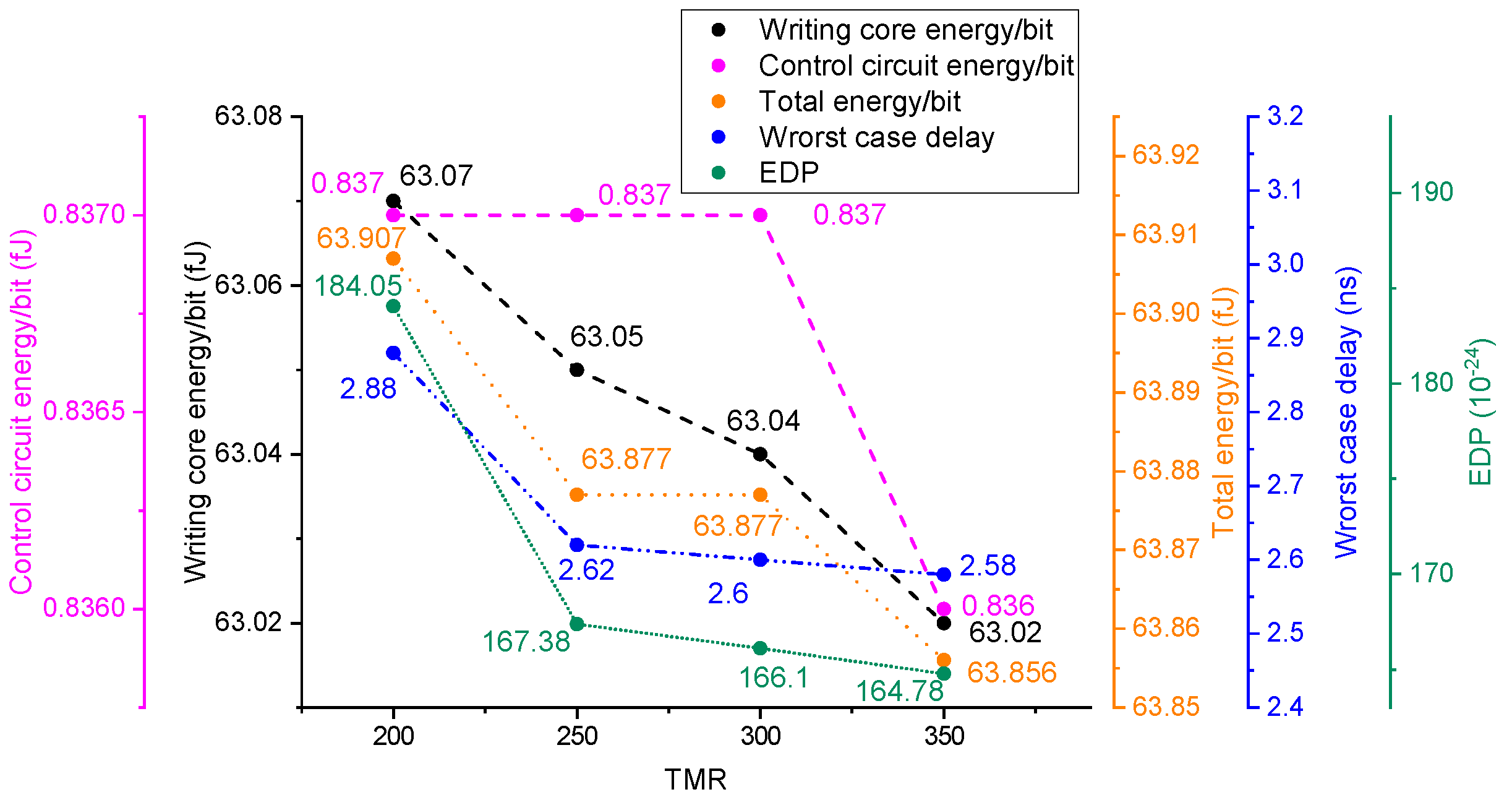
| Design Type | Min | Max | Mean | Std Divination |
|---|---|---|---|---|
| Writing core energy/bit (fJ) | 56.52 | 67.08 | 62.33 | 2.782 |
| Control circuit energy/bit (fJ) | 0.749 | 0.883 | 0.833 | 0.031 |
| Total energy/bit (fJ) | 57.269 | 67.963 | 63.163 | 2.813 |
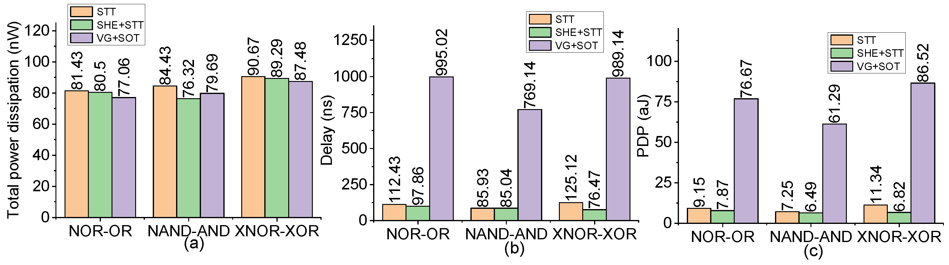
| Gate | NOR-OR | NAND-AND | XNOR-XOR | ||||||
|---|---|---|---|---|---|---|---|---|---|
| p-MTJ | STT | SHE+STT | VG+SOT | STT | SHE+STT | VG+SOT | STT | SHE+STT | VG+SOT |
| Static | 0 | 0 | 0 | 0 | 0 | 0 | 0 | 0 | 0 |
| power (nW) | (55.83 ) | (53.51 ) | (68.16 ) | (55.48 ) | (53.99 ) | (62.96 ) | (57.92 ) | (58.89 ) | (68.14 ) |
| Dynamic power (nW) | 25.59 | 26.99 | 8.9 | 28.95 | 28.33 | 16.72 | 32.75 | 30.4 | 19.34 |
| Total power (nW) | 81.42 | 80.5 | 77.06 | 84.43 | 82.32 | 79.68 | 90.67 | 89.29 | 87.48 |
| Delay (ps) | 112.43 | 97.86 | 995.02 | 85.93 | 85.04 | 769.14 | 125.12 | 76.47 | 989.14 |
| PDP (aJ) | 9.15 | 7.87 | 76.67 | 7.25 | 7 | 61.28 | 11.34 | 6.82 | 86.52 |
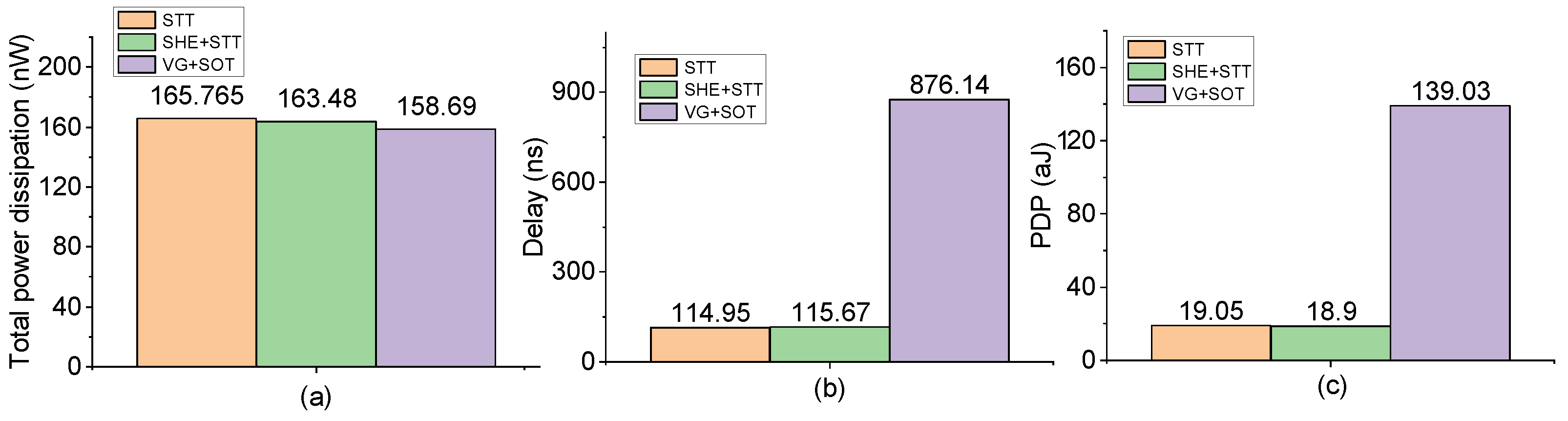
| NVFA | STT | SHE+STT | VG+SOT |
|---|---|---|---|
| Static power (nW) | 0 (119.4 ) | 0 (119.75 ) | 0 (145.7 ) |
| Dynamic power (nW) | 46.36 | 43.73 | 12.99 |
| Total power (nW) | 165.76 | 163.48 | 158.69 |
| Delay (ps) | 114.95 | 115.67 | 876.14 |
| PDP (aJ) | 19.05 | 18.9 | 139.03 |
Disclaimer/Publisher’s Note: The statements, opinions and data contained in all publications are solely those of the individual author(s) and contributor(s) and not of MDPI and/or the editor(s). MDPI and/or the editor(s) disclaim responsibility for any injury to people or property resulting from any ideas, methods, instructions or products referred to in the content. |
© 2024 by the authors. Licensee MDPI, Basel, Switzerland. This article is an open access article distributed under the terms and conditions of the Creative Commons Attribution (CC BY) license (https://creativecommons.org/licenses/by/4.0/).
Share and Cite
Barla, P.; Shivarama, H.; Deepa, G.; Ujjwal, U. Design and Assessment of Hybrid MTJ/CMOS Circuits for In-Memory-Computation. J. Low Power Electron. Appl. 2024, 14, 3. https://doi.org/10.3390/jlpea14010003
Barla P, Shivarama H, Deepa G, Ujjwal U. Design and Assessment of Hybrid MTJ/CMOS Circuits for In-Memory-Computation. Journal of Low Power Electronics and Applications. 2024; 14(1):3. https://doi.org/10.3390/jlpea14010003
Chicago/Turabian StyleBarla, Prashanth, Hemalatha Shivarama, Ganesan Deepa, and Ujjwal Ujjwal. 2024. "Design and Assessment of Hybrid MTJ/CMOS Circuits for In-Memory-Computation" Journal of Low Power Electronics and Applications 14, no. 1: 3. https://doi.org/10.3390/jlpea14010003