Article

Multi-Ported GC-eDRAM Bitcell with Dynamic Port Configuration and Refresh Mechanism †

1
Emerging Nanoscaled Integrated Circuits and Systems (EnICS) Labs, Faculty of Engineering, Bar-Ilan University, Ramat Gan 5290002, Israel
2
Telecommunications Circuits Laboratory (TCL), École Polytechnique Fédérale de Lausanne (EPFL), 1015 Lausanne, Switzerland
*
Author to whom correspondence should be addressed.
This paper is an extended version of our paper published in IEEE International Conference on Electronics, Circuits, and Systems.
J. Low Power Electron. Appl. 2024, 14(1), 2; https://doi.org/10.3390/jlpea14010002
Submission received: 9 September 2023 / Revised: 13 December 2023 / Accepted: 27 December 2023 / Published: 4 January 2024

Abstract

:
Embedded memories occupy an increasingly dominant part of the area and power budgets of modern systems-on-chips (SoCs). Multi-ported embedded memories, commonly used by media SoCs and graphical processing units, occupy even more area and consume higher power due to larger memory bitcells. Gain-cell eDRAM is a high-density alternative for multi-ported operation with a small silicon footprint. However, conventional gain-cell memories have limited data availability, as they require periodic refresh operations to maintain their data. In this paper, we propose a novel multi-ported gain-cell design, which provides up-to N read ports and M independent write ports (NRMW). In addition, the proposed design features a configurable mode of operation, supporting a hidden refresh mechanism for improved memory availability, as well as a novel opportunistic refresh port approach. An 8kbit memory macro was implemented using a four-transistor bitcell with four ports (2R2W) in a 28 nm FD-SOI technology, offering up-to a 3× reduction in bitcell area compared to other dual-ported SRAM memory options, while also providing 100% memory availability, as opposed to conventional dynamic memories, which are hindered by limited availability.

1. Introduction

As CMOS technology continues to scale, high density embedded memories are of great interest for modern microprocessors and other VLSI system-on-chip (SoC) designs. In fact, embedded memories often dominate the total area and power budget of entire SoCs [1]. Various blocks that are integrated on these SoCs, such as media, graphics processing units, and computational cores, require multi-ported embedded memories to improve their bandwidth by enabling multiple operations using the same memory bank in parallel. For example, the dual-port memory is well utilized for video processing units because several read and write access operations are possible at the same time [2,3]. A larger number of read ports is also utilized in graphics processors, in machine learning applications [4], and as shared system level memory that provides simultaneous access to multiple devices [5,6]. A large number of write ports can be found in multi-threaded applications [7] and vector processors. These, and many other applications and systems, raise the need for N-ported memory design [8,9,10,11,12,13].
The majority of conventional embedded memories are based on the single-ported six-transistor (6T) static random access memory (SRAM) bitcell, shown in Figure 1a. This cell is popular thanks to its symmetrical structure, robust operation, and quick generation using dedicated SRAM compilers. The 6T bitcell utilizes a pair of cross-coupled inverters (M1/M3 and M4/M6) for static data storage and provides read/write access through a pair of access transistors (M2 and M5). This pair of access devices supports either a single read or a single write operation during a given clock cycle, and therefore it is considered to have a single port, also denoted as “1RW” [3]. While architectural techniques, such as array duplication, can be applied to provide more than one read or write per clock cycle, larger bitcells are required to achieve true multi-ported functionality, resulting in significant area and power overheads [13,14]. Commonly found examples of such bitcells include the eight-transistor dual-ported cell of Figure 1b, which has two pairs of access transistors to provide two completely independent read and write operations (2RW); the eight-transistor two-ported cell, shown in Figure 1c, that comprises a decoupled read port (M7/M8) to enable simultaneous read and write accesses (1R1W) [3]; and the ten-transistor cell, shown in Figure 1d, which has two decoupled read ports that can be used to enable two reads and one write (2R1W) in a parallel or a single differential read [2].
Examples of bitcells with a higher number of ports include the 24-transistor SRAM bitcell of [6] and the 16-transistor bitcell of [5]. The former, illustrated in Figure 2a, provides 6R2W functionality, achieving improved read stability by adding drivers between Q/QB and the read ports to improve the read static noise margin (SNM). The latter, illustrated in Figure 2b, provides 5R1W functionality using several dedicated read ports. Another recently suggested SRAM-based bitcell is the 8R1W 20T bitcell [4] targeting deep learning applications, illustrated in Figure 2c. This bitcell has a separated differential write port, two drain-connected single transistor read ports, and six gate-connected read ports with two transistors. Half of the read ports are connected to Q and the other half are connected to QB. The inverted read can be flipped by single inverter connected to the column output. Another suggested approach is performing double-pumped read and write operations as suggested in [12,16]. For example, applying this technique to a 3R3W bitcell in [16] transforms it into a 6R6W bitcell. While this technique significantly reduces the bitcell area and macro routing due to a lower number of word-lines and bit-lines, it requires a complex control system and an internal Clock Pulse Generator (CPG). Additionally, the cell requires fast read and write operations, adding additional design constraints. A bitcell suggested for double pumping is illustrated in Figure 3. However, beyond these, bitcells with more than two read ports are almost unaddressed and can hardly be found in the literature, and the SRAM bitcells, presented in [4,5,6], come at a high cost in area and often result in decreased SNMs as a result of the additional read ports. Another approach to multiported memory design is standard cell-based memory which utilizes Data Flip-Flop (DFF) or D-latch cells as memory elements [17]. While this technique has low design costs, it comes at the cost of very large area and power overhead [13,18,19].
Another actively researched approach in many core computing applications is utilizing the system interconnect for storing the data in local single ported caches to improve the memory accessibility. While this approach provides throughput improvement up to 2.5 ×  [20,21], it requires complex cache coherency management and large area overhead. An additional similar approach is near memory computing that places the memory macros near the computational units, both reducing the cost of driving the data to the module and also allowing each computational unit to have exclusive access to the data it requires. This approach is very compatible with machine learning (ML) and data encryption and decryption operations [22]. Often, such works embed processing elements within the memory to achieve what is commonly referred to as “in-memory computing” [23,24,25]. Memories constructed with emerging devices, such as resistive and magnetic RAM, are commonly used for this purpose [26,27,28]. An example of such a work is described in [29], where highly efficient storage of model weights and personalized data is securely achieved using such memories. Interfacing with these dedicated memories very often requires multi-ported functionality [30,31,32].
As a high-density alternative with inherent two-ported functionality, gain-cell embedded DRAM (GC-eDRAM) has become increasingly popular in recent years [33,34,35,36,37,38]. In addition to providing their 1R1W functionality, these memories provide a non-destructive read operation and low leakage power within a small silicon footprint. Moreover, compared to conventional 1T-1C eDRAM, gain cells are fully logic-compatible, not requiring any non-standard process steps to fabricate the cell capacitance. Recent work has focused on using GC-eDRAM as an area-efficient storage element for embedded in-memory computing applications [39,40,41,42,43]. However, as a dynamic memory, periodic refresh operations are required for data retention, limiting the memory availability.
In this paper, we propose a novel GC-eDRAM bitcell topology constructed with ( N + M ) transistors ( [ N + M ] T) to simultaneously provide up to N independent reads and M independent writes (NRMW). The proposed memory has several modes of operation: NRMW mode provides ( N + M ) -ported functionality at a very low area and power cost, utilizing a single transistor as a write or read port; and [ N 1 ] R [ M 1 ] W mode, which can be used to hide refresh operations from the outer architecture to provide 100% memory availability. As such, the proposed design provides an area-efficient solution for the realization of multi-ported memories, such as digital signal processing, machine learning, and advanced microprocessors. The opportunistic refresh port mode is suggested for maximizing memory utilization when a large number of ports is required, since it allows us to partially hide the refresh operations by utilizing temporarily unused ports during standard NRMW operation. To demonstrate the proposed topology, an 8 kbit memory array based on a novel 4T bitcell offering 2R2W [15] capabilities was implemented in a 28 nm FD-SOI technology, providing between 1.8–3× area reduction compared to other dual-ported SRAM memories, while maintaining 100% memory availability.

Contributions

The major contributions of this paper are summarized as follows:
  • This work presents the first reported 2R2W and 6R2W GC-eDRAM memory, as well as a general design guideline for N-ported dynamic memories.
  • The resulting bitcell is the smallest multi-ported memory reported in the literature.
  • A novel opportunistic refresh port approach for dynamic memory arrays with NRMW access ports is provided.
  • The proposed array can be dynamically configured to support an internal refresh operation without sacrificing memory availability.
The rest of this paper is structured as follows: Section 2 presents the proposed multi-ported circuit design and operating mechanism; implementation and extensive post-layout simulation results of the NRMW cell are provided in Section 3; memory configurations and operating modes are presented in Section 4; Section 5 compares the proposed memory to other multi-ported memory options; and Section 6 concludes the paper.

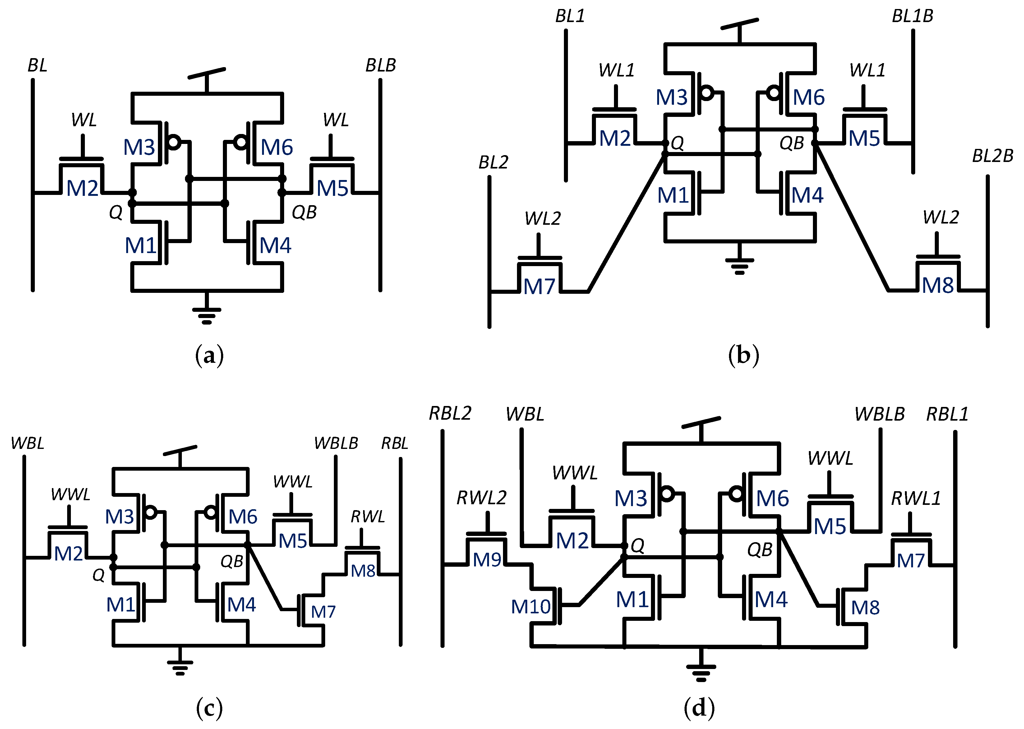
2. Multi-Ported Gain Cell Design

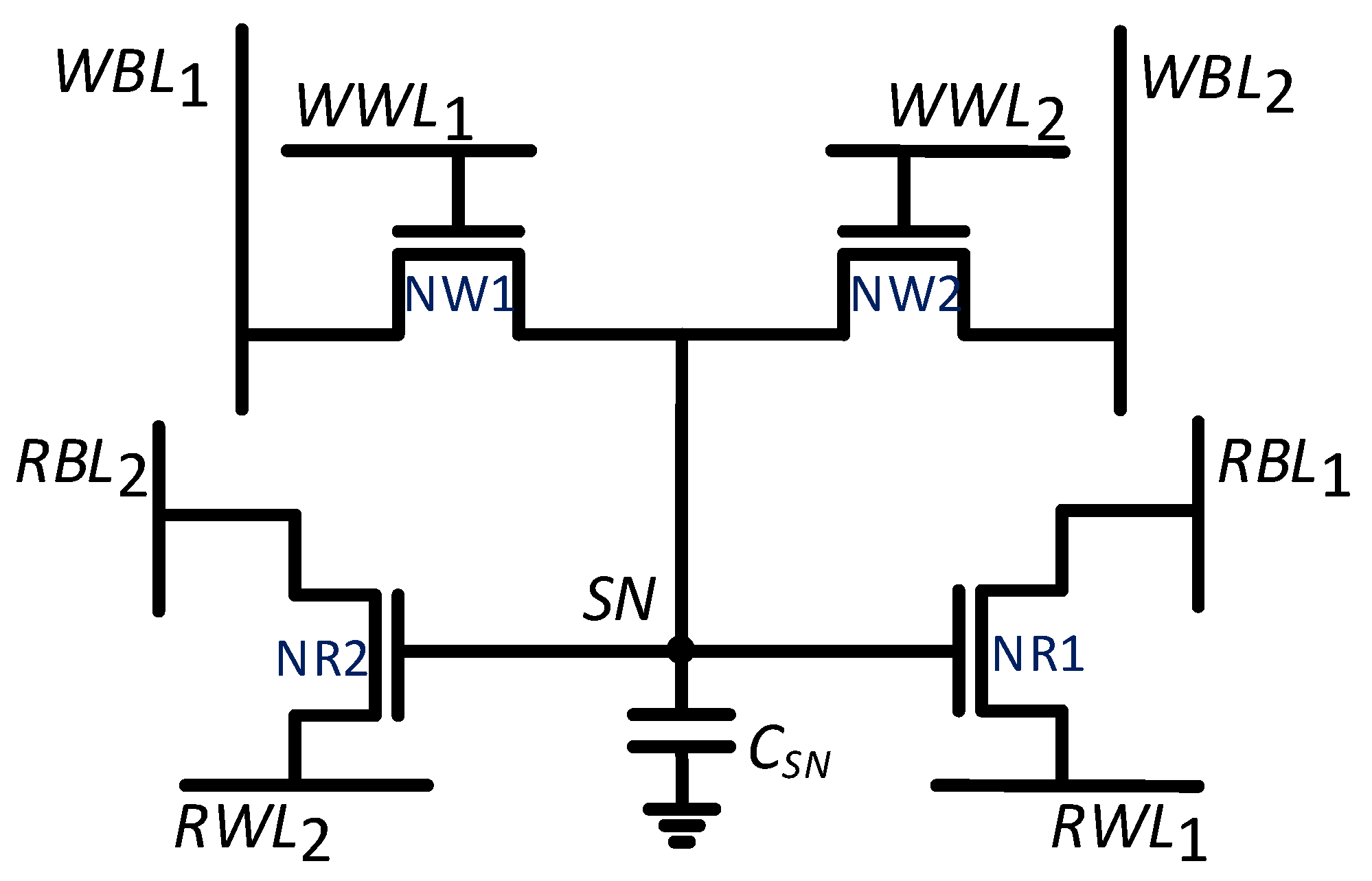
2.1. 2R2W Cell Design and Operating Mechanism

A 2R2W gain-cell, designed with four transistors, is shown in Figure 4. This circuit is based on the general concept of the NRMW GC-eDRAM cell design. As the least complex example of the proposed topology, this cell will be used as a reference design throughout the paper for demonstrating the memory properties. The circuit comprises two write ports featuring n-type MOSFET (NMOS) write access devices (NW1 and NW2) and two read ports, based on NMOS read access devices (NR1 and NR2). NMOS devices were preferred over p-type MOSFET (PMOS) devices due to faster access times [35]. In write mode, the write bit-line (WBL 1 or WBL 2 ) voltage is transferred to the storage node through its corresponding write access device (NW1 or NW2, respectively) when the appropriate write word-line signal (WWL 1 or WWL 2 , respectively) is asserted. The write word lines are asserted by driving them to a boosted voltage (1.2 V) to enable passing a strong logic-‘1’ into the cell. The separation of the two write ports with independent write word-lines and write bit-lines provides the cell with 2W capability. During standby and read-only cycles, the write word-lines are discharged to −200 mV in order to suppresses the sub-threshold leakage from the storage node (SN) and extend the data retention time (DRT) [44].
In read mode, the appropriate read bit-line (RBL 1 or RBL 2 ) is first pre-charged to V DD while the read word-line is kept closed (at V DD ). In the second phase of the read, its corresponding read word-line (RWL 1 or RWL 2 , respectively) is discharged to GND. The corresponding read bit-line is then discharged if the cell is storing a logic-‘1’, or otherwise remains charged to represent a logic-‘0’. Similar to write, the separation of the two read ports with independent read word-lines and read bit-lines provides the capability to achieve two parallel reads (2R) to complete the aforementioned 2R2W functionality.
The functionality of the proposed bitcell is demonstrated through the waveforms of Figure 5. The figure shows a simultaneous write operation to two bitcells at two different addresses, writing ‘0’ to one cell and ‘1’ to the second cell. These write operations are followed by simultaneous reads from the previously written addresses. It is clearly shown that RBL 1 is discharged to a value close to one threshold-voltage drop below the supply ( V DD V T ), as its corresponding bitcell is storing a logic-‘1’, and similarly RBL 2 remains at the precharge level of V DD , as its corresponding bitcell is storing a logic-‘0’. In total, four independent rows of the array can be activated in parallel, enabling two separate write and two separate read operations to be performed simultaneously. When two conflicting (opposite) data values are written to the cell, the memory gives priority to port 1 (WWL 1 /WBL 1 ), disabling the write access to the second port.

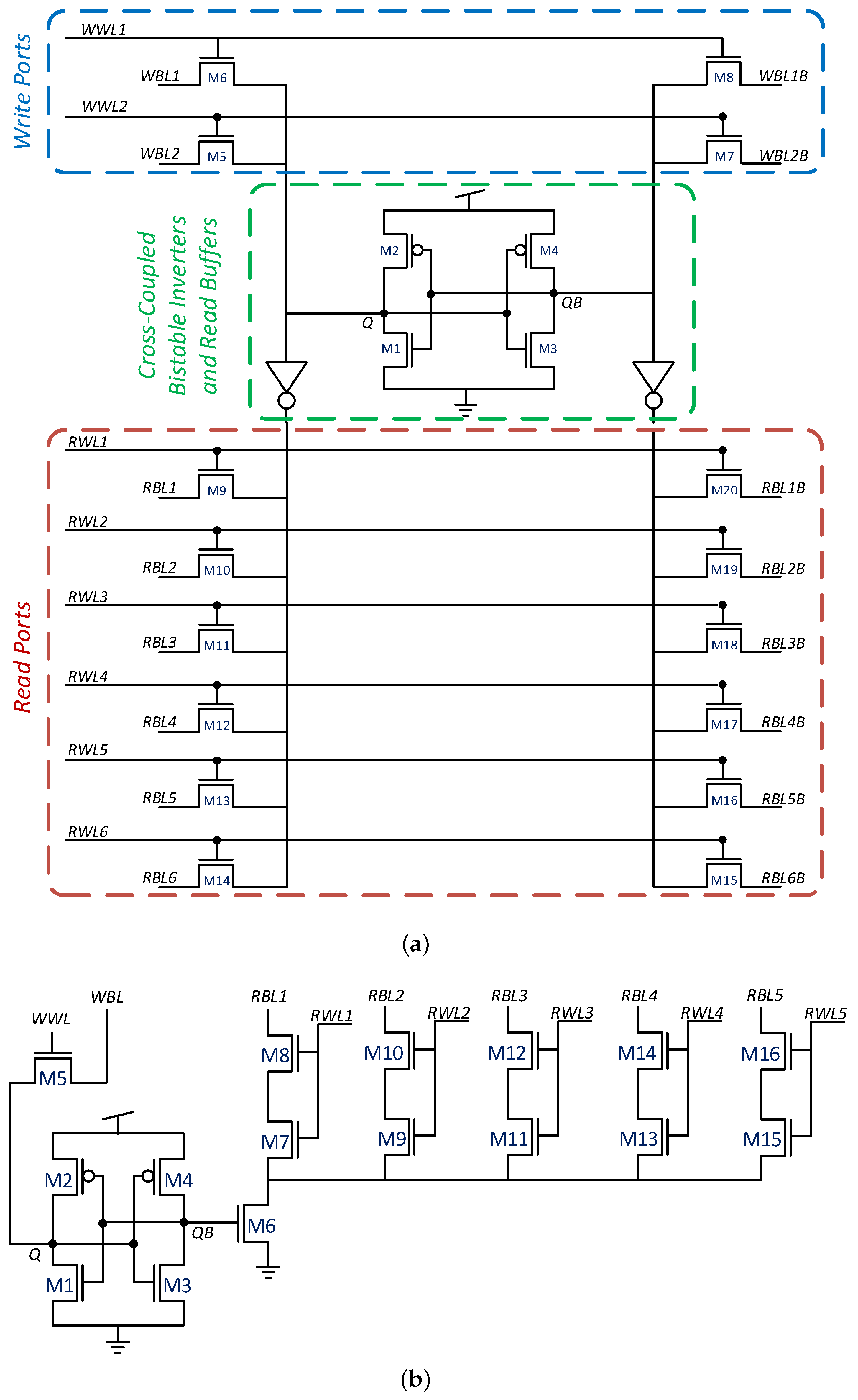
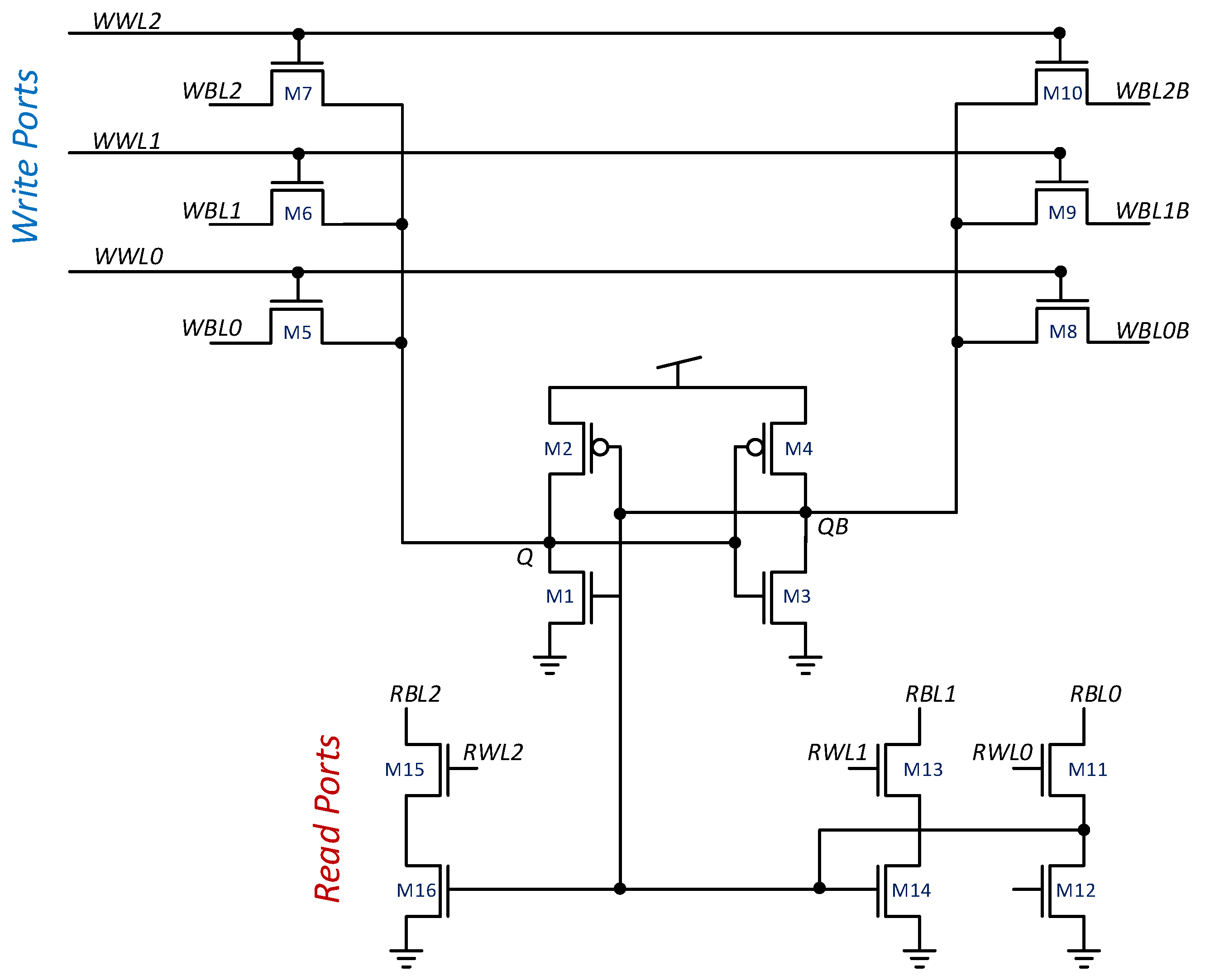
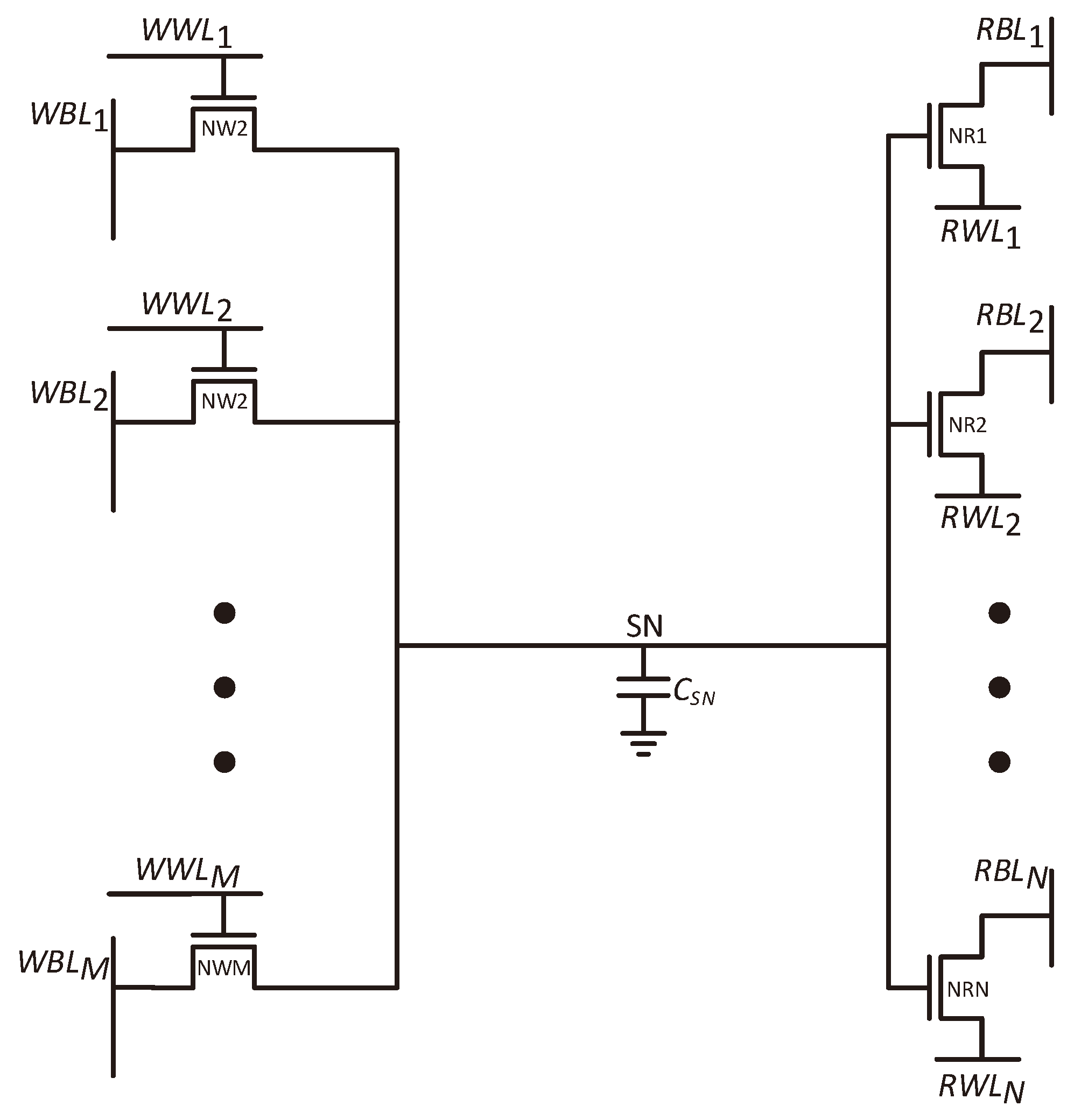
2.2. Expanding the Number of Read Ports

Multi-ported embedded memories with more than two read ports are even more beneficial for high-bandwidth applications [6]. Yet, due to large size and increased complexity of the SRAM implementations [5], these cells are uncommon [13]. Existing SRAM implementations are area costly and rely on decoupling the read ports from the cell itself, as shown in Figure 2a, for performing differential or single ended reads from those ports.
The proposed GC-eDRAM topology enables the design of an ( N + M ) -ported memory, using only ( N + M ) transistors. For comparison, the eight-ported 6R2W memory, reported in [6], required 24 transistors, whereas the proposed topology achieves the same functionality using only 8 transistors. The same operating principle, demonstrated for the 2R2W cell, is maintained here. Every additional transistor is a standalone read or write port. Since the multi-ported read functionality is the more common requirement, in this work we focused on expanding the number of read ports. Nevertheless, expanding the number of write ports in the proposed cell design can also be achieved by adding a single transistor for each additional write port.
A cell with N read ports will have N read word lines, indexed from RWL 1 to RWL N , with each word-line connected to the source of a corresponding read transistor, and N read bitlines, indexed from RBL 1 to RBL N , connected to the drain of the same corresponding read transistor. In a similar way, M write port word lines are indexed WWL 1 to WWL M and are connected to corresponding write transistor gates, while M write bitlines, indexed from WBL 1 to WBL M , are connected to the drains of these write transistors. The proposed cell structure is presented in Figure 6. Due to the decoupled nature of GC-eDRAM circuits, each write and read port operates independently, without affecting the operation of the other ports. When two conflicting (opposite) data values are written to the cell, the memory gives priority to port 1 (WWL 1 /WBL 1 ). Due to the nature of gain cell design, in which the data is stored on the parasitic capacitance of the gates of the read transistors, simultaneous read of the same row by all ports is allowed and does not affect performance.

3. Implementation and Simulation Results

In order to evaluate the proposed cell design characteristics, a representative 2R2W bitcell was implemented in a fully-depleted silicon-on-insulator (FD-SOI) technology, using regular- V T (RVT) NMOS transistors, which were preferred over low- V T (LVT) devices due to lower cell leakage. This section will overview the implementation and simulation results. Layout considerations for expanding the number of read ports are also described in this section.

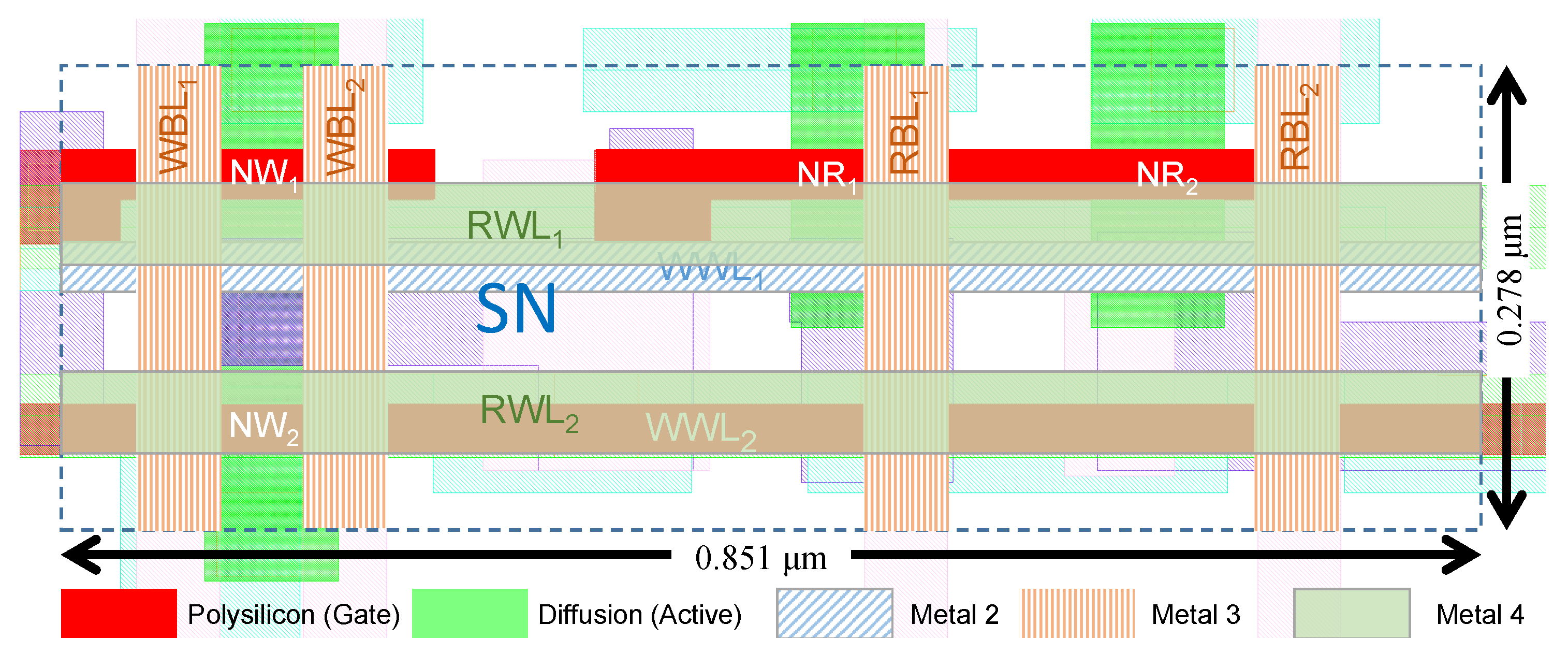
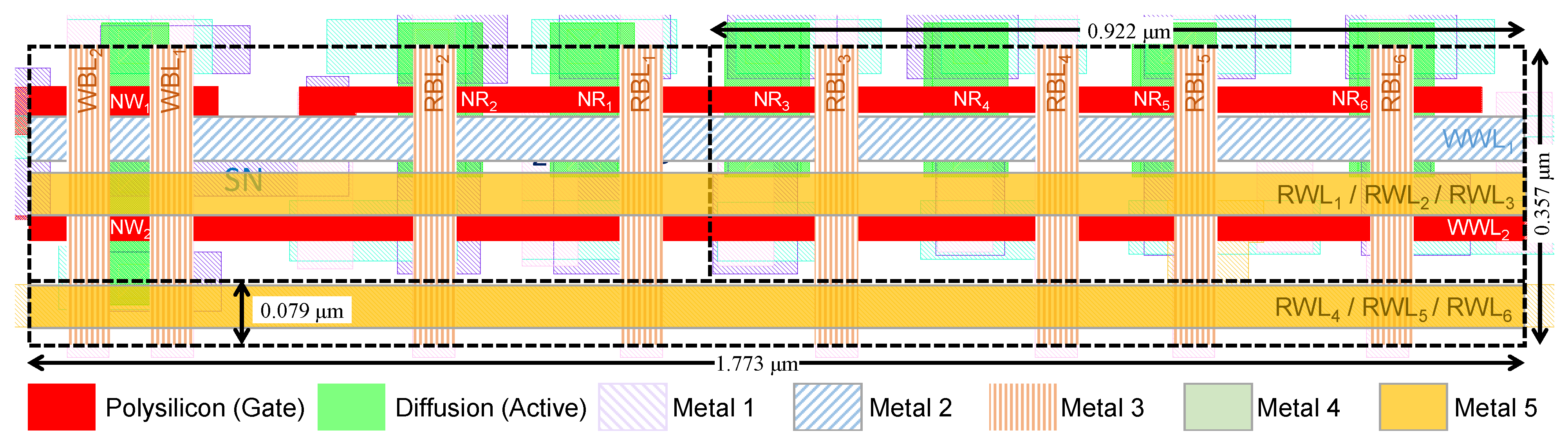
3.1. 2R2W Bitcell Layout

Layout of the 2R2W bitcell is shown in Figure 7, measured at 0.24 μm2 (0.851 μm × 0.278 μm). The cell layout features WWL1 and WWL2 routed with horizontal poly and Metal-2 lines for reduced capacitance and better area utilization, respectively. RWL1 and RWL2 were routed with a horizontal Metal-4 stripe, and the bit-lines were routed with a vertical Metal-3 stripe. Metal-2 is mainly used in cell routing. The access transistor connected to WWL2 has a larger gate length than the access transistor connected to WWL1 to reduce leakage. This port is also better for usage in the 1R1W mode for leakage reduction, as the write speed is not a limiting factor for the memory frequency [34].

3.2. Expanding the Layout to Accommodate Additional Read Ports

While any combination of read and write ports can be achieved in the proposed topology, the high density of the cell makes the signal routing the dominant consideration in the cell design. Additional cell area is required for routing the RWL signals, and higher metal layers are used to optimize the cell area utilization. Designing a cell with three additional read ports requires enlarging the height of the cell in order to accommodate the additional RWL metal stripes.
To demonstrate such a cell layout, the layout of an 8T-6R2W cell is illustrated in Figure 8, measured at 0.63 μm2 (1.773 μm × 0.357 μm). In order to add four additional read ports to the design, RWL1, RWL2, and RWL3 were routed above the transistors, and RWL4, RWL5, and RWL6 were routed through Metal-4, 5, and 6 stripes at the bottom of the cell. These metal stripes require adding 0.079 μm to the 2R2W cell height. The additional four read transistors enlarge the 2R2W cell width by 0.922 μm.
Note that, since Metal-6 is often required for global power routing, avoiding its usage in the memory macro is possible at the cost of adding an additional 0.18 μm2 to the cell area. Yet, as the GC-eDRAM is typically a self-contained block and the bitcells do not require power rail connections, routing through Metal-6 may be acceptable for improving memory density.
The symmetric layout of the cell allows us to derive a formula for cell area (A) based on the number of read and write ports:
A ( N , M ) [ μ m 2 ] = N + M 8 , M 2 : ( 0.278 + 0.079 · N 4 ) · ( 0.851 + ( N 2 ) · T h p ) N + M 8 , M > 2 : 0.477 · ( 0.851 + ( N 2 ) · T h p + ( M 2 ) · ( T h p + D p ) ) N + M > 8 : ( 0.357 + 2.2 · W M x · N + M 6 3 ) · ( 0.851 + ( N 2 ) · T h p + ( M 2 ) · ( T h p + D p ) )
where W M x denotes the minimal metal width for the technology, defined as 0.05 μm for this process; D p is defined as the minimal distance between two poly stripes, measured at 0.096 μm for this process; and T h p is the horizontal pitch of minimal sized transistor for the given technology (including the gate tap), derived at 0.23 μm for this process.
The layout of Figure 8 shows how to route the signals of the added ports, according to the formula. While the upper third of the cell layout utilizes the routing tracks for in-cell connections, the middle and bottom thirds are primarily used to route the horizontal wordlines, going up to Metal-5. Each set of three wordlines can be routed across a single horizontal track by breaking the middle signal to allow space for vias that vertically connect the signals to the corresponding front-end connections. Following this approach, adding up to three additional wordlines requires extending the cell height by only 0.11 μm, and this can be repeated for any number of additional ports. Furthermore, each additional read transistor requires adding 0.23 μm to the cell width, and each additional write transistor requires adding 0.36 μm to the cell width. The difference between adding read and write transistors is derived from the constraint that write port poly cannot be shared and each gate needs its own tap, while for read transistors the poly is shared and they all connect to the same tap.
The numeric parameters in the formula are also technology dependent and calculated as follows: 0.278 μm is the minimum height that the two write transistors (sharing a diffusion) can fit; 0.851 μm is the width of the 2R2W cell comprised from 3 T h p , D p , and additional routing area; 0.079 μm is the added height for word lines 4–6 and derived from W M x . Yet, since the joined write transistors are wider than the metals required for word, the area added by word lines 4–6 is reduced.
A comparison of the area of the proposed topology to other multi-ported designs is provided in Figure 9. The area of the multi-ported 6R2W bit-cell, illustrated in Figure 8, is only 1.9× bigger than the single ported 1WR SRAM cell, and when operating in the 1W5R mode, described in Section 4, it is 2.73× smaller than the corresponding SRAM cell described in [5].

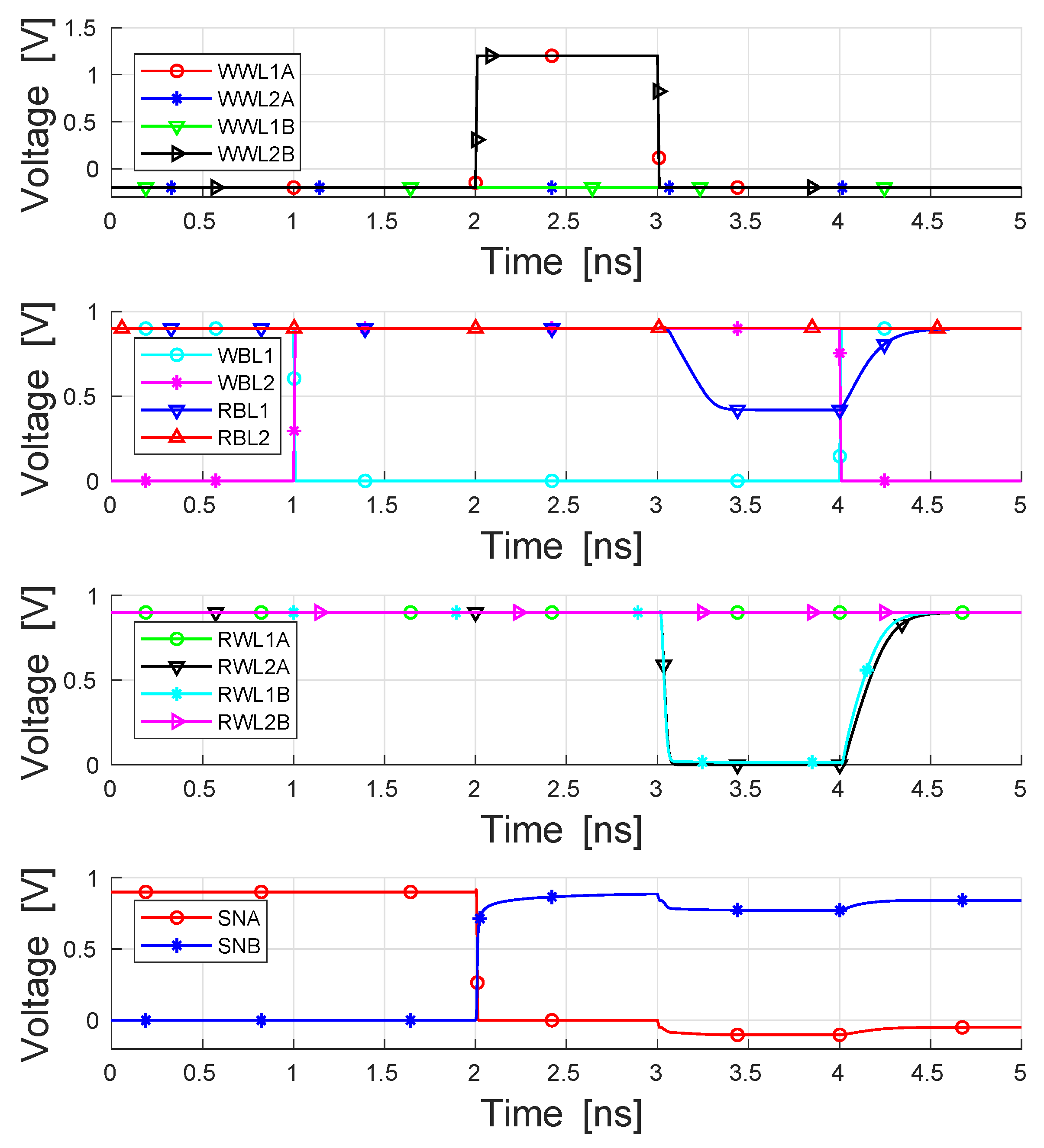
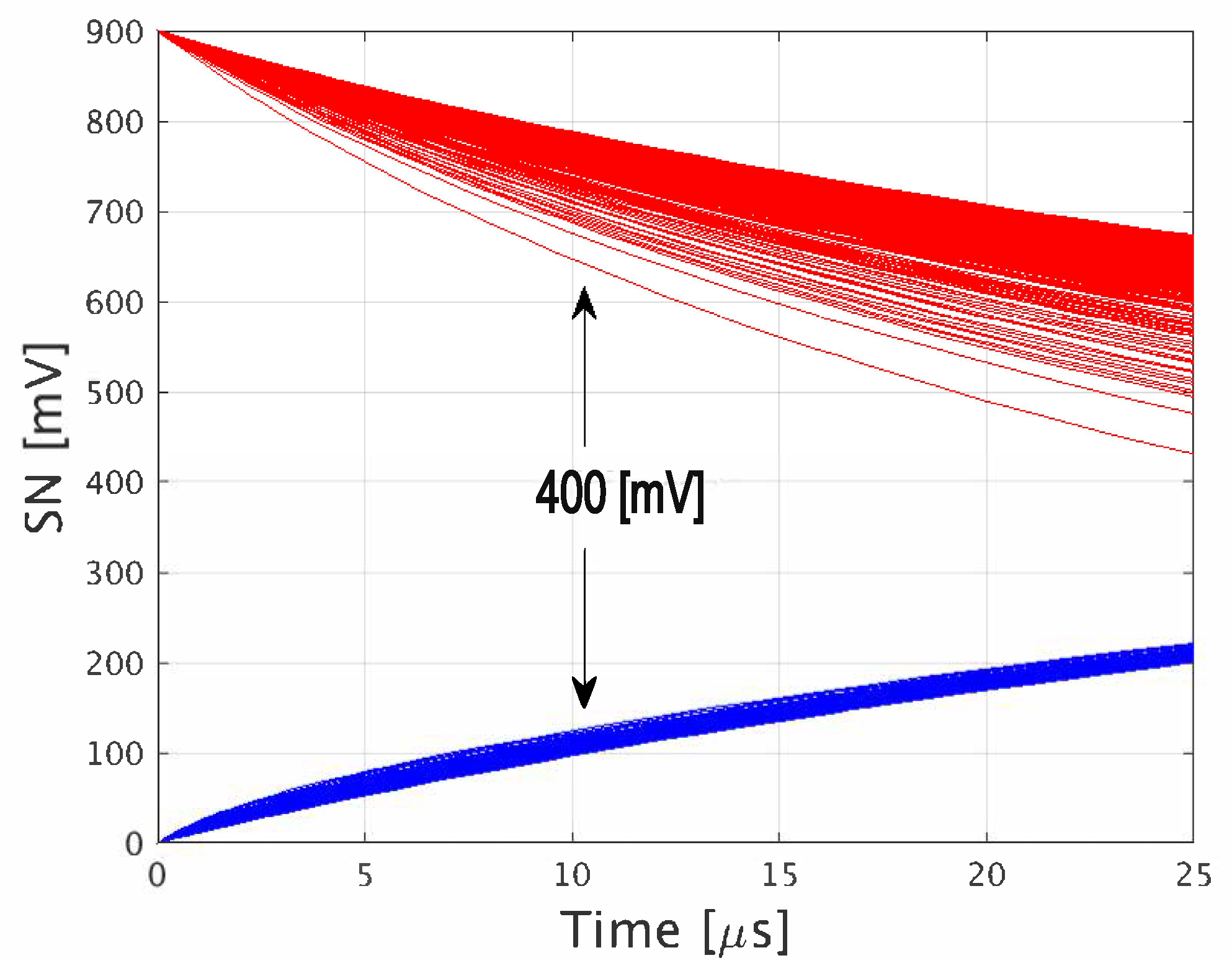
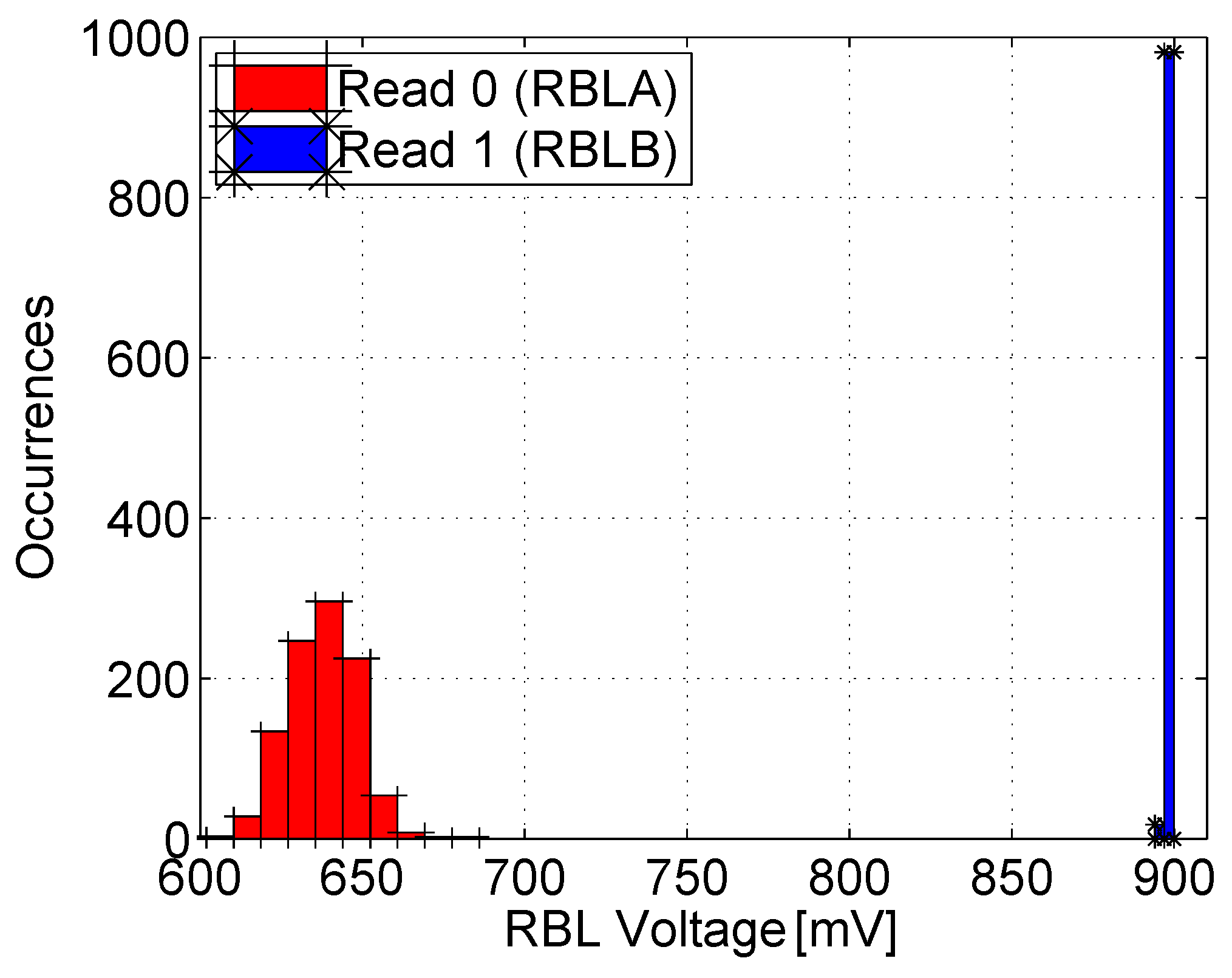
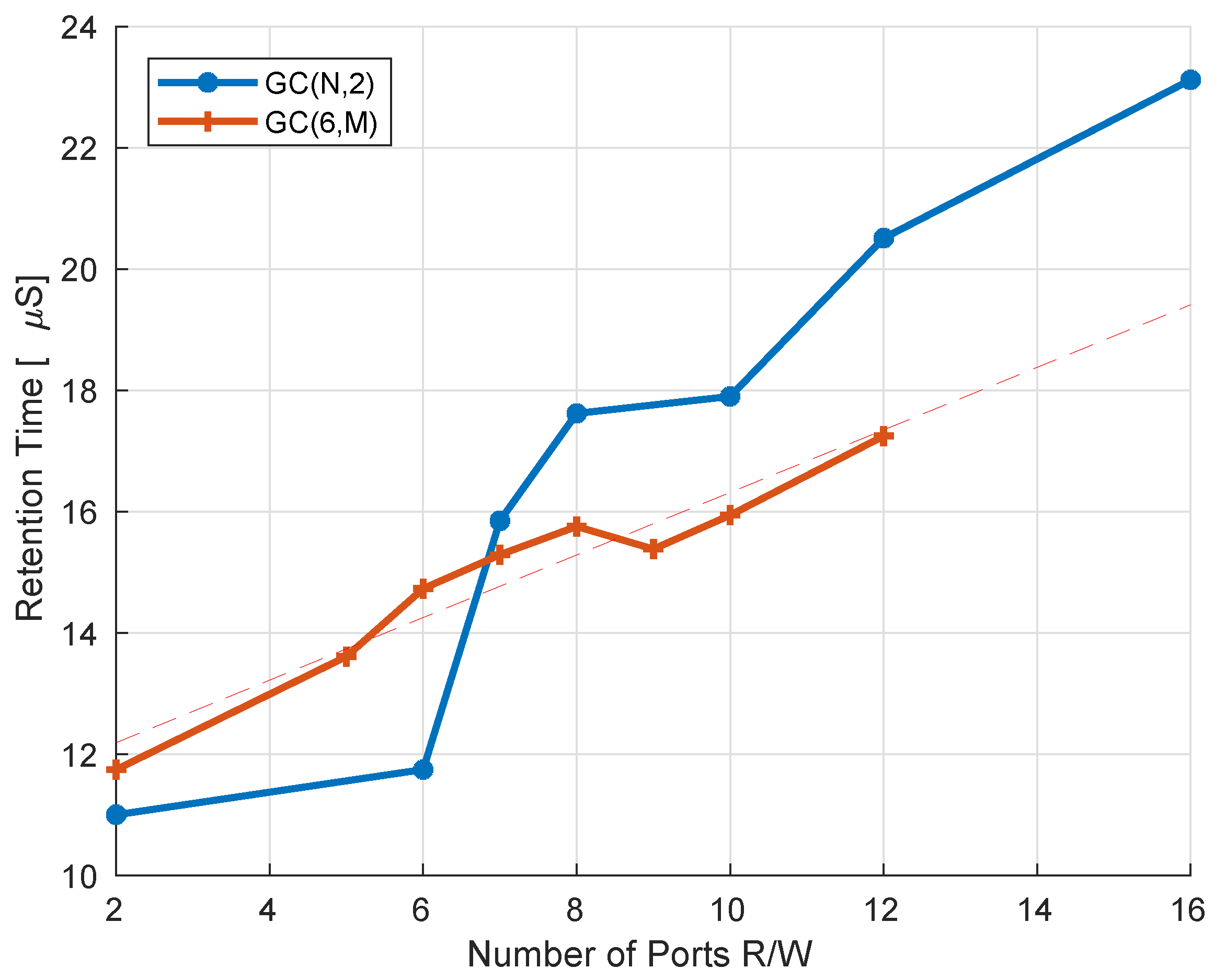
3.3. Simulation Results

To quantify the characteristics of the proposed cell design, a 128 × 64 bit (8 kbit) memory macro, based on the reference 2R2W cell, was designed in a 28 nm FD-SOI process, and simulated under a 900 mV supply voltage at room temperature. All simulations were carried out with Cadence Virtuoso, using the Spectre circuit simulator, based on post-layout simulations applied to extracted views including parasitics. Retention time testbenches and estimations were performed according to the methodologies elaborated upon in [34].
In order to estimate the DRT of the implemented array, 1000 Monte Carlo (MC) statistical simulations, including mismatch and process variations, were applied to extract the deterioration of the storage node voltage following a write operation. The simulations were run under worst-case biasing conditions when operated in the 2R2W mode, i.e., WBL1 and WBL2 were biased to the opposite voltage of that stored on the SN to maximize the leakage current of the cell. The resulting deterioration curves of SN are shown in Figure 10, indicating a worst-case DRT of 6 μs, defined at the time when the difference between data ‘1’ and ‘0’ reaches beneath 400 mV.
To verify the readability of the bitcell, Figure 11 shows the distribution of the RBL voltage following read ‘0’ and read ‘1’ operations with a cycle time of 2 ns (500 MHz) following a 6 μs retention period. This plot was also extracted from 1000 post-layout MC simulations with mismatch modeling and including the layout-extracted parasitics. The simulations were run under worst-case conditions with all the unselected cells in the column storing a ‘1’. This disables the RBLs to discharge to ‘0’ when reading ‘1’ due to leakage from the unselected cells, causing the RBL to saturate slightly above 600 mV. Nevertheless, the voltage distributions of the RBL, when reading ‘1’ and ‘0’, are clearly separated, indicating that the array can be correctly read following the target retention period, with the switching threshold of the sense inverter positioned between the RBL distributions. The 6R2W multi-ported version of the bitcell demonstrates similar results.
The performance of the read ports is exactly the same as in the 2R2W version of the cell, since they are completely independent of each other. The write ports are slightly slower due to the increased SN capacitance, yet since the write operation is much faster than the read, as illustrated in Figure 5, the overall performance is unchanged. Retention time on the other hand is increased as we add additional read or write ports, as illustrated in Figure 12. For example, increasing the number of read ports from six to sixteen yields an almost 2× retention time improvement. In terms of SN capacitance, increasing the number of write ports from two to twelve will result in an increase from 0.5 fF to 1.6 fF. Increasing the number of read ports is more efficient in terms of retention time since we increase the SN capacitance by adding poly-silicon area, at a cost of a relatively small gate leakage. When we increase the number of write ports, in addition to the increased storage node capacitance, we also have additional leakage sources through the added write transistor gates. Overall, the access performance of the suggested cell design does not change as a result of increasing the number of ports, while the increased retention time for a large number of ports improves the memory availability.
The leakage power of the 2R2W cell, simulated under worst-case biasing conditions, was found to be 0.93 pW/bit and 1.2 pW/bit for the 6R2W cell. The worst case biasing conditions are different between the cells since for the 6R2W bitcell, the read ports gate leakage becomes more substantial than the write ports gate leakage. The active refresh energy was found to be 65 fJ/bit, composed of 25 fJ/bit for read and 40 fJ/bit for write.

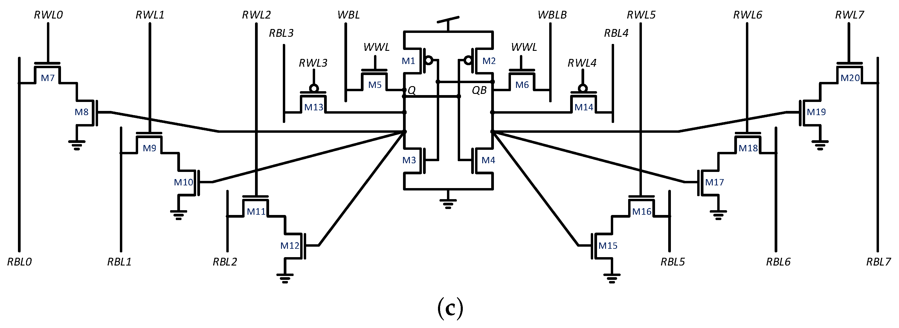
4. Configurable Operation

The previous sections demonstrated that the proposed bitcell can be operated as a NRMW bitcell, with N read ports and M write ports, focusing on a detailed evaluation of the 2R2W implementation of this topology, and the implications of adding additional read and write ports. In this section, we will show how the bitcell can be dynamically configured for optimization of the system memory usage.

4.1. NRMW Operation Mode

The standard operation mode of the proposed topology, as presented earlier, provides NRMW functionality for high-bandwidth applications that require multi-ported operation, where as many as N simultaneous reads and M simultaneous writes (NRMW) are needed. This is achieved by utilizing each pair of write word-lines and write bit-lines (WWL1/WBL1, WWL2/WBL2 up to WWLM/WBLM) for write operations, and each pair of read word-lines and read bit-lines (RWL1/RBL1, RWL2/RBL2 up to RWLN/RBLN) for read operations. While N + M separate row-decoders are required to support this extensive functionality, the requirement can be reduced to fewer row decoders. For example, in regards to the 4T cell presented in Section 2.1, if dual-ported (2RW) operation is sufficient, the number of decoders can be reduced to two decoders. As mentioned before, there is no conflict between the ports and all the ports can operate simultaneously without a performance penalty. When operated in NRMW mode, the bitcell may still require periodic refresh operations, yet for the suggested design, min ( N , M ) ports can be used in parallel to perform the refresh, at the cost of memory blockage for ( R + 1 ) / min ( N , M ) clock cycles, where R is the number of rows in the array. This improves the memory availability for arrays with a large number of access ports.

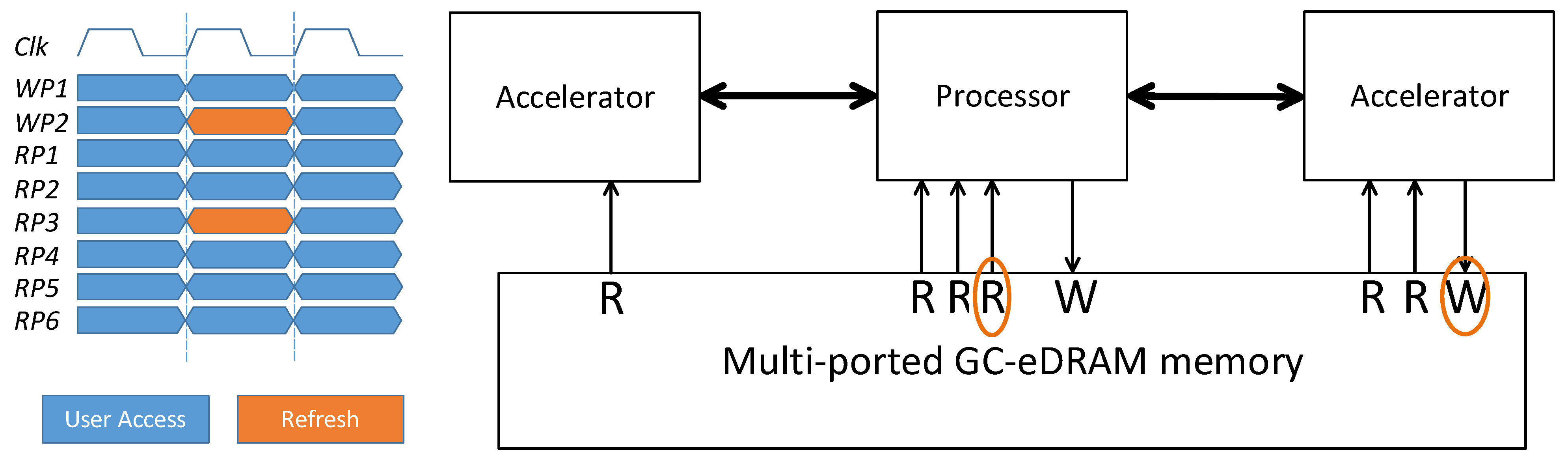
4.2. Internal Refresh Mode

Dynamic memories, such as GC-eDRAM, suffer from limited DRT due to leakage currents through the storage node. The deterioration of the data levels under worst-case biasing conditions is shown in Figure 10, with the DRT defined at the point where the logic-‘1’ (red lines) and logic-‘0’ (blue lines) intersect. In order to ensure data integrity, refresh operations, which read out and write back all the data in the memory array, are periodically applied. In addition to the refresh power consumption, the memory availability is compromised, since the memory is unavailable for external accesses when refresh is applied. This would render the proposed memory incompatible with certain applications that cannot tolerate such occurrences.
To address this issue, the proposed design includes a unique configuration capability, which can provide inherent 100% array availability at the expense of a reduction in the number of available ports. In this mode, the NRMW capability is reduced—at least temporarily—to ( N 1 ) R ( M 1 ) W, and the other ports are used for hidden refresh of the array. This loss of capability can be tolerated by applications that do not need the full NRMW functionality, while still providing at least a two-ported (1R1W) memory that can be used as a direct replacement for sram with both area and power reductions, while avoiding the need to integrate special controllers or dedicated refresh-aware protocols. These kinds of techniques are often applied for DRAM memories, where the many-word rows and longer read latency allow even further customization. These techniques are often referred to as parallel and hidden refresh, where the refresh operation is hidden inside the DRAM controller by design [45,46,47,48,49].
To apply the hidden refresh mode, low indexed ports WWL1/WBL1 and RWL1/RBL1 up to WWL M 1 /WBL M 1 and RWL N 1 /RBL N 1 are used to perform the standard write and read operations, respectively, as requested by the system. A refresh controller that is provided along with the memory macro and transparent to the outer architecture uses the last set of ports, WWLM/WBLM and RWLN/RBLN, to perform the refresh operation. In this way, the refresh is hidden from the outer system and applied without interfering with standard multi-ported array accesses. The area overhead of the dedicated refresh ports is almost negligible for cells with a large number of ports. For example, when implementing a 10R8W bitcell, the dedicated refresh ports will consume only 11% of the cell area. Note that if the system is not required to dynamically reconfigure the memory, the last set of address decoders can be replaced by a simple shift-register-based state machine to carry out the refresh operations. In addition, the DRT of the array is slightly higher than in NRMW mode, as the bias value can be controlled during non-refresh cycles and set at the best-case level.

4.3. High Performance Opportunistic Refresh Port Mode

The multi-ported nature of the NRMW bitcell allows us to combine the multi-ported refresh approach, explained in Section 4.1, with the hidden refresh mode to enable an opportunistic refresh port approach. This approach dynamically chooses a read or write port that is not being used by the system in the current cycle, and uses it as a read or write port for refresh. In this mode, instead of completely blocking the ports used for refresh, the memory controller waits until one of the ports becomes available (i.e., not used by the system), and performs a refresh operation using this port. This technique reduces the percentage of time the memory is blocked for read or write, from ( α r + α w ) of opportunistic refresh algorithm such as [50], down to ( α r / N + α w / M ), where α r and α w denote the memory refresh read and write blockage during normal system operation. For the case of the 2R2W cell (the minimal proposed configuration), the availability is improved by 50%.
The suggested refresh controller operation is described in Algorithm 1. It is based on using an available read port for reading the refreshed row into a buffer, and later—when there is an available write port—writing it back. The main principle of the suggested algorithm is to use any free port it can find for the refresh operation. The operations on read and write ports are performed in parallel (denoted by “⇒”) as all the ports are completely independent. While the write port algorithm is a straightforward search for an available write port to use for the refresh, the read ports operation is more complex. Since a single buffer is used both for storing the read data and writing from it, it can be read into in only one of the following two cases:
  • The previous data is written back into the array at the current cycle.
  • There is no data in the buffer.
Algorithm 1 Refresh Controller Algorithm
  • for ever do
  •    // Wait until next refresh
  •      c y c l e s = 0
  •     while  c y c l e s < D R T _ c y c l e s · S E _ F a c t o r  do
  •          c y c l e s + +
  •    // Perform opportunistic refresh
  •      r e a d _ r o w = 0
  •      w r i t e _ r o w = 0
  •     while  w r i t e _ r o w < N R O W S  do
  •         ⇒if  data   stored   in   buffer  do
  •            for each in W R I T E _ P O R T S  do
  •                if  P O R T is f r e e  then
  •                    write data from buffer to w r i t e _ r o w
  •                     w r i t e _ r o w + +
  •                     break
  •         ⇒for  e a c h   i n   R E A D   P O R T S  do
  •            if  P O R T is f r e e  then
  •                if buffer is empty or RW_cycle then
  •                    read data from r e a d _ r o w to b u f f e r
  •                     r e a d _ r o w + +
  •               break
  •          c y c l e s   + +
  •         if not  c y c l e s   <   D R T _ c y c l e s  then
  •            break
  •    // Check opportunistic refresh success
  •     if  w r i t e _ r o w     N R O W S  then
  •         initiate blocking refresh
Since read access time is typically the frequency limiting factor, in case there is data stored in the buffer, we do not want to wait for the logic that checks for write port availability before searching for a free read port. Instead, we look for a free read port in parallel to looking for a free write port, and read the new data only if the buffer is empty or the stored data is written in the current cycle (i.e., a free write port is found, denoted by R W _ c y c l e ). In case the controller fails to complete the refresh in the time slot given to the opportunistic refresh, a blocking sequential refresh is enforced on the system, in a similar way to other opportunistic algorithms [50,51,52,53].
This refresh scheme can be extremely useful for systems in which different devices are connected to different ports, such as the architecture suggested in [7] where the memory is connected in up to six parallel execution units. In such a configuration, there will be gaps in memory utilization at the system level, during which a certain peripheral does not use the memory. This time can be used as an opportunity for the memory controller to perform refresh operations without disturbing the system, almost completely eliminating memory blockages. An example of such a system configuration is illustrated in Figure 13, where the suggested memory is implemented for a 2W6R configuration. For this design, we assume that one accelerator (on the right) requires one write port and two read ports, and the other accelerator (on the left) requires a single read port. The controller detects cycles when there is no access from an external interface to one of the ports and internally utilizes this memory port to perform the required refresh operation. It should be noted that for configurations with several write ports, the controller has to keep track to ensure there are no write collisions and that the row in which data is stored in the buffer has not been overwritten since the read. In case the row is overwritten by external access, the buffer should be discarded and the next row should be read.

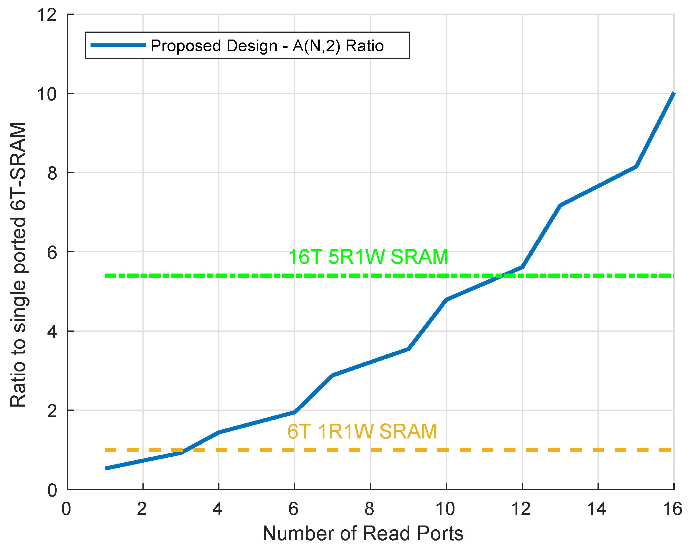
5. Comparison to SRAM

Table 1 shows a comparison between the proposed 4T 2R2W bitcell and other multi-ported embedded memory options, including a 2T gain-cell [34], 6T SRAM [54], 8T SRAM [3], and a 10T SRAM [2,55]. A major advantage of the proposed cell over other dual-ported SRAM implementations is in the cell area size, offering between a 1.8–3× reduction over the compared SRAM implementations with the same number of ports. While the 2T gain-cell offers the lowest area, it only provides two-ported (1R1W) operation, as compared to the 2R2W functionality offered by the smallest configuration of the proposed topology. Moreover, while the 2T gain-cell provides almost the same DRT as the proposed 2R2W cell, it has a reduced memory availability of 97.3% due to the refresh operation occupying the single write and read ports. Alternatively, if operated in the internal-refresh (1R1W) mode, the proposed topology provides 100% availability. This is a significant advantage over standard GC-eDRAM offerings, as it simplifies the system design and enables straightforward replacement of SRAM with GC-eDRAM memories.
Table 2 compares the many-ported implementations. Three different bitcells based on the suggested design are compared with SRAM-based options. The first comparison is for a 5R1W bitcell that is compared with a 16T SRAM-based bitcell [5]. The second comparison is between 8R1W implementations; our implementation compared to a 20T SRAM-based bitcell [4]. Finally, a 12T 6R6W Gain Cell is compared with the 16T 3W3R SRAM-based bitcell, which is pumped to 6R6W functionality in [16]. Even though the GC-eDRAM bitcell is compared with a bitcell that has half the number of ports, the GC-eDRAM area savings are significant. This can be explained by the symmetrical and NMOS-only based design of the GC-eDRAM memory. Moreover, techniques such as double-pumping are rarely applicable, since the memory itself is often the performance bottleneck in the system, and if the memory can go faster, it is more beneficial to activate the whole system at a higher frequency.
The area advantage becomes even more substantial when comparing an NRMW configuration to other multi-ported offerings. A 6R2W configuration of the proposed topology is only 1.9× larger than a standard 1RW SRAM cell. When compared to a cell with similar functionality, the proposed 6R2W configuration in internal-refresh mode provides 5R1W functionality, while being 2.8× smaller than the 5R1W SRAM cell of [5]. Moreover, while multi-ported SRAM requires special techniques to maintain sufficient noise margins during read operations (e.g., [6]), the decoupled read of the proposed GC-eDRAM multi-ported configuration allows for adding any number of read ports for simultaneous operation. For a larger number of ports, the improved DRT and availability completely eliminate the disadvantages of the GC-eDRAM, making it a superior multi-ported solution over SRAM.

6. Conclusions

This paper proposed a novel multi-ported gain-cell eDRAM bitcell topology that provides up to N simultaneous read and M simultaneous write (NRMW) operations for use in high-bandwidth applications that require several memory operations in parallel. The configuration of some of these ports for applying internal refresh provides the opportunity to use the proposed topology as a straightforward SRAM replacement with 100% memory availability. By further exploiting the unused ports for opportunistic refresh, the memory availability can be maximized while maintaining near NRMW functionality. Compared to other dual-ported SRAM memory options, the proposed 2R2W cell provides between 1.8–3× area reduction and the lowest leakage power consumption, providing much higher savings as compared to memories with more ports. Compared to conventional GC-eDRAM memories, the multi-ported cell configured for internal-refresh offers 100% memory availability, overcoming one of the main drawbacks of dynamic memory solutions.

Author Contributions

Conceptualization, R.G. (Roman Golman) and R.G. (Robert Giterman); analysis, simulation, and writing, R.G. (Roman Golman); supervision, review and editing, A.T. All authors have read and agreed to the published version of the manuscript.

Funding

This work was funded by the Israel Ministry of Science, Innovation and Technology (MOST) under the the Lise Meitner Grants for Israeli-Swedish Research Collaboration Project “AutoPiM”.

Data Availability Statement

Restrictions apply to the availability of these data. Data was based on intellectual property of third parties accessed under non-disclosure agreements.

Conflicts of Interest

The authors declare no conflict of interest.

References

  1. IEEE. International Technology Roadmap for Semiconductors (IRDS)—2023 Update. 2023. Available online: https://irds.ieee.org/editions/2023 (accessed on 26 December 2023).
  2. Noguchi, H.; Okumura, S.; Iguchi, Y.; Fujiwara, H.; Morita, Y.; Nii, K.; Kawaguchi, H.; Yoshimoto, M. Which is the Best Dual-Port SRAM in 45-nm Process Technology? 8T, 10T single end, and 10T differential. In Proceedings of the ICICDT 2008, Grenoble, France, 2–4 June 2008; pp. 55–58. [Google Scholar]
  3. Nii, K.; Tsukamoto, Y.; Yabuuchi, M.; Masuda, Y.; Imaoka, S.; Usui, K.; Ohbayashi, S.; Makino, H.; Shinohara, H. Synchronous ultra-high-density 2RW dual-port 8T-SRAM with circumvention of simultaneous common-row-access. IEEE J. Solid-State Circuits 2009, 44, 977–986. [Google Scholar] [CrossRef]
  4. Ohara, R.; Masaya, K.; Taichi, M.; Fukunaga, A.; Yasuda, Y.; Hamabe, R.; Izumi, S.; Kawaguchi, H. A 1W8R 20T SRAM Codebook for 20% Energy Reduction in Mixed-Precision Deep-Learning Inference Processor System. In Proceedings of the 2023 IEEE 5th International Conference on Artificial Intelligence Circuits and Systems (AICAS), Hangzhou, China, 11–13 June 2023; pp. 1–5. [Google Scholar] [CrossRef]
  5. Hsiao, S.; Wu, P. Design of low-leakage multi-port SRAM for register file in graphics processing unit. In Proceedings of the 2014 IEEE International Symposium on Circuits and Systems (ISCAS), Melbourne, VIC, Australia, 1–5 June 2014; pp. 2181–2184. [Google Scholar] [CrossRef]
  6. Ataei, S.; Gaalswyk, M.; Stine, J.E. A high performance multi-port SRAM for low voltage shared memory systems in 32 nm CMOS. In Proceedings of the 2017 IEEE 60th International Midwest Symposium on Circuits and Systems (MWSCAS), Boston, MA, USA, 6–9 August 2017; pp. 1236–1239. [Google Scholar] [CrossRef]
  7. Fetzer, E.S.; Dahle, D.; Little, C.; Safford, K. The Parity protected, multithreaded register files on the 90-nm itanium microprocessor. IEEE J. Solid-State Circuits 2006, 41, 246–255. [Google Scholar] [CrossRef]
  8. Abdelhadi, A.M.S.; Lemieux, G.G.F. A Multi-ported Memory Compiler Utilizing True Dual-Port BRAMs. In Proceedings of the 2016 IEEE 24th Annual International Symposium on Field-Programmable Custom Computing Machines (FCCM), Washington, DC, USA, 1–3 May 2016; pp. 140–147. [Google Scholar] [CrossRef]
  9. Tseng, J.H.; Asanovic, K. Banked multiported register files for high-frequency superscalar microprocessors. In Proceedings of the 30th Annual International Symposium on Computer Architecture, San Diego, CA, USA, 9–11 June 2003; pp. 62–71. [Google Scholar] [CrossRef]
  10. Chang, P.Y.; Lin, T.J.; Wang, J.S.; Yu, Y.H. A 4R/2W Register File Design for UDVS Microprocessors in 65-nm CMOS. IEEE Trans. Circuits Syst. II Express Briefs 2012, 59, 908–912. [Google Scholar] [CrossRef]
  11. Zhang, X.; Li, Y.; Xiong, B.; Han, J.; Zhang, Y.; Dong, F.; Zhang, Z.; Yu, Z.; Cheng, X.; Zeng, X. Robust and low power register file in 65 nm technology. J. Semicond. 2012, 33, 035010. [Google Scholar] [CrossRef]
  12. Ditlow, G.S.; Montoye, R.K.; Storino, S.N.; Dance, S.M.; Ehrenreich, S.; Fleischer, B.M.; Fox, T.W.; Holmes, K.M.; Mihara, J.; Nakamura, Y.; et al. A 4R2W register file for a 2.3 GHz wire-speed POWER™ processor with double-pumped write operation. In Proceedings of the 2011 IEEE International Solid-State Circuits Conference, San Francisco, CA, USA, 20–24 February 2011; pp. 256–258. [Google Scholar]
  13. Marinberg, H.; Garzón, E.; Noy, T.; Lanuzza, M.; Teman, A. Efficient Implementation of Many-Ported Memories by Using Standard-Cell Memory Approach. IEEE Access 2023, 11, 94885–94897. [Google Scholar] [CrossRef]
  14. Kulkarni, J.P.; Keane, J.; Koo, K.H.; Nalam, S.; Guo, Z.; Karl, E.; Zhang, K. 5.6 Mb/mm2 1R1W 8T SRAM Arrays Operating Down to 560 mV Utilizing Small-Signal Sensing with Charge Shared Bitline and Asymmetric Sense Amplifier in 14 nm FinFET CMOS Technology. IEEE J. Solid-State Circuits 2017, 52, 229–239. [Google Scholar] [CrossRef]
  15. Golman, R.; Giterman, R.; Teman, A. Configurable Multi-Port Dynamic Bitcell with Internal Refresh Mechanism. In Proceedings of the 2018 25th IEEE International Conference on Electronics, Circuits and Systems (ICECS), Bordeaux, France, 9–12 December 2018; pp. 589–592. [Google Scholar]
  16. Nguyen, H.; Jeong, J.; Atallah, F.; Yingling, D.; Bowman, K. A 7-nm 6R6W Register File With Double-Pumped Read and Write Operations for High-Bandwidth Memory in Machine Learning and CPU Processors. IEEE Solid-State Circuits Lett. 2018, 1, 225–228. [Google Scholar] [CrossRef]
  17. Kadomoto, J.; Irie, H.; Sakai, S. Multiport Register File Design for High-Performance Embedded Cores. In Proceedings of the 2021 IEEE 14th International Symposium on Embedded Multicore/Many-core Systems-on-Chip (MCSoC), Singapore, 20–23 December 2021; pp. 281–286. [Google Scholar] [CrossRef]
  18. Andersson, O.; Mohammadi, B.; Meinerzhagen, P.; Burg, A.; Rodrigues, J.N. Ultra Low Voltage Synthesizable Memories: A Trade-Off Discussion in 65 nm CMOS. IEEE Trans. Circuits Syst. I Regul. Pap. 2016, 63, 806–817. [Google Scholar] [CrossRef]
  19. Fan, X.; Stuijt, J.; Liu, B.; Gemmeke, T. Synthesizable Memory Arrays Based on Logic Gates for Subthreshold Operation in IoT. IEEE Trans. Circuits Syst. I Regul. Pap. 2019, 66, 941–954. [Google Scholar] [CrossRef]
  20. Ramesh, T.; Abed, K. Reconfigurable Many-Core Embedded Computing Platform with Geometrical Bus Interconnection. In Proceedings of the 2020 International Conference on Computational Science and Computational Intelligence (CSCI), Las Vegas, NV, USA, 16–18 December 2020; pp. 1256–1259. [Google Scholar] [CrossRef]
  21. Ramesh, T.; Abed, K. An efficient multi-level cache system for geometrically interconnected many-core chip multiprocessor. Int. J. Reconfigurable Embed. Syst. 2022, 11, 93. [Google Scholar] [CrossRef]
  22. Zhang, C.; Sun, H.; Li, S.; Wang, Y.; Chen, H.; Liu, H. A Survey of Memory-Centric Energy Efficient Computer Architecture. IEEE Trans. Parallel Distrib. Syst. 2023, 34, 2657–2670. [Google Scholar] [CrossRef]
  23. Wu, P.C.; Su, J.W.; Chung, Y.L.; Hong, L.Y.; Ren, J.S.; Chang, F.C.; Wu, Y.; Chen, H.Y.; Lin, C.H.; Hsiao, H.M.; et al. A 28nm 1Mb Time-Domain Computing-in-Memory 6T-SRAM Macro with a 6.6ns Latency, 1241GOPS and 37.01TOPS/W for 8b-MAC Operations for Edge-AI Devices. In Proceedings of the 2022 IEEE International Solid-State Circuits Conference (ISSCC), San Francisco, CA, USA, 20–26 February 2022; Volume 65, pp. 1–3. [Google Scholar] [CrossRef]
  24. Si, X.; Chen, J.J.; Tu, Y.N.; Huang, W.H.; Wang, J.H.; Chiu, Y.C.; Wei, W.C.; Wu, S.Y.; Sun, X.; Liu, R.; et al. 24.5 A Twin-8T SRAM Computation-In-Memory Macro for Multiple-Bit CNN-Based Machine Learning. In Proceedings of the 2019 IEEE International Solid-State Circuits Conference—(ISSCC), San Francisco, CA, USA, 17–21 February 2019; pp. 396–398. [Google Scholar] [CrossRef]
  25. Dong, Q.; Sinangil, M.E.; Erbagci, B.; Sun, D.; Khwa, W.S.; Liao, H.J.; Wang, Y.; Chang, J. 15.3 A 351TOPS/W and 372.4GOPS Compute-in-Memory SRAM Macro in 7 nm FinFET CMOS for Machine-Learning Applications. In Proceedings of the 2020 IEEE International Solid-State Circuits Conference—(ISSCC), San Francisco, CA, USA, 16–20 February 2020; pp. 242–244. [Google Scholar] [CrossRef]
  26. Garzon, E.; Yavits, L.; Lanuzza, M.; Teman, A. Emerging Memory Structures for VLSI Circuits. In Wiley Encyclopedia of Electrical and Electronics Engineering; Wiley: Hoboken, NJ, USA, 2022. [Google Scholar] [CrossRef]
  27. Hung, J.M.; Xue, C.X.; Kao, H.Y.; Huang, Y.H.; Chang, F.C.; Huang, S.P.; Liu, T.W.; Jhang, C.J.; Su, C.I.; Khwa, W.S.; et al. A four-megabit compute-in-memory macro with eight-bit precision based on CMOS and resistive random-access memory for AI edge devices. Nat. Electron. 2021, 4, 921–930. [Google Scholar] [CrossRef]
  28. Wei, Q.; Gao, B.; Tang, J.; Qian, H.; Wu, H. Emerging Memory-Based Chip Development for Neuromorphic Computing: Status, Challenges, and Perspectives. IEEE Electron. Devices Mag. 2023, 1, 33–49. [Google Scholar] [CrossRef]
  29. Chiu, Y.C.; Yang, C.S.; Teng, S.H.; Huang, H.Y.; Chang, F.C.; Wu, Y.; Chien, Y.A.; Hsieh, F.L.; Li, C.Y.; Lin, G.Y.; et al. A 22nm 4Mb STT-MRAM Data-Encrypted Near-Memory Computation Macro with a 192GB/s Read-and-Decryption Bandwidth and 25.1-55.1TOPS/W 8b MAC for AI Operations. In Proceedings of the 2022 IEEE International Solid-State Circuits Conference (ISSCC), San Francisco, CA, USA, 20–26 February 2022; Volume 65, pp. 178–180. [Google Scholar] [CrossRef]
  30. Biswas, A.; Chandrakasan, A.P. Conv-RAM: An energy-efficient SRAM with embedded convolution computation for low-power CNN-based machine learning applications. In Proceedings of the 2018 IEEE International Solid-State Circuits Conference—(ISSCC), San Francisco, CA, USA, 11–15 February 2018; pp. 488–490. [Google Scholar] [CrossRef]
  31. Nguyen, V.T.; Kim, J.S.; Lee, J.W. 10T SRAM Computing-in-Memory Macros for Binary and Multibit MAC Operation of DNN Edge Processors. IEEE Access 2021, 9, 71262–71276. [Google Scholar] [CrossRef]
  32. Chen, Y.; Mu, J.; Kim, H.; Lu, L.; Kim, T.T.H. A Reconfigurable 8T SRAM Macro for Bit-Parallel Searching and Computing In-Memory. In Proceedings of the 2022 IEEE International Symposium on Circuits and Systems (ISCAS), Austin, TX, USA, 27 May–1 June 2022; pp. 2556–2560. [Google Scholar] [CrossRef]
  33. Kang, G.; Choi, W.; Park, J. Embedded DRAM-Based Memory Customization for Low-Cost FFT Processor Design. IEEE Trans. Very Large Scale Integr. Syst. 2017, 25, 3484–3494. [Google Scholar] [CrossRef]
  34. Meinerzhagen, P.; Teman, A.; Giterman, R.; Edri, N.; Burg, A.; Fish, A. Gain-Cell Embedded DRAMs for Low-Power VLSI Systems-on-Chip; Springer International Publishing: Cham, Switzerland, 2018. [Google Scholar]
  35. Giterman, R.; Fish, A.; Burg, A.; Teman, A. A 4-Transistor nMOS-Only Logic-Compatible Gain-Cell Embedded DRAM With Over 1.6-ms Retention Time at 700 mV in 28-nm FD-SOI. IEEE Trans. Circuits Syst. I 2017, 65, 1245–1256. [Google Scholar] [CrossRef]
  36. Giterman, R.; Fish, A.; Geuli, N.; Mentovich, E.; Burg, A.; Teman, A. An 800-MHz Mixed-VT 4T IFGC Embedded DRAM in 28-nm CMOS Bulk Process for Approximate Storage Applications. IEEE J. Solid-State Circuits 2018, 53, 2136–2148. [Google Scholar] [CrossRef]
  37. Harel, O.; Casarrubias, E.N.; Eggimann, M.; Gürkaynak, F.; Benini, L.; Teman, A.; Giterman, R.; Burg, A. 64kB 65nm GC-eDRAM with Half-Select Support and Parallel Refresh Technique. IEEE Solid-State Circuits Lett. 2022, 5, 170–173. [Google Scholar] [CrossRef]
  38. Hsieh, E.R.; Huang, C.F.; Huang, S.Y.; Miu, M.L.; Lu, S.M.; Wu, Y.S.; Ye, Y.H. A Logic Fully Comparable Single-Supply Capacitor-Less 1-FinFET-1-Source-Channel-Drain-Diode (1T1D) Embedded DRAM MACRO in 16-nm FinFET. IEEE Solid-State Circuits Lett. 2023, 6, 249–252. [Google Scholar] [CrossRef]
  39. Xie, S.; Ni, C.; Sayal, A.; Jain, P.; Hamzaoglu, F.; Kulkarni, J.P. 16.2 eDRAM-CIM: Compute-In-Memory Design with Reconfigurable Embedded-Dynamic-Memory Array Realizing Adaptive Data Converters and Charge-Domain Computing. In Proceedings of the 2021 IEEE International Solid-State Circuits Conference (ISSCC), San Francisco, CA, USA, 13–22 February 2021; Volume 64, pp. 248–250. [Google Scholar] [CrossRef]
  40. Chen, Z.; Chen, X.; Gu, J. 15.3 A 65 nm 3T Dynamic Analog RAM-Based Computing-in-Memory Macro and CNN Accelerator with Retention Enhancement, Adaptive Analog Sparsity and 44TOPS/W System Energy Efficiency. In Proceedings of the 2021 IEEE International Solid-State Circuits Conference (ISSCC), San Francisco, CA, USA, 13–22 February 2021; Volume 64, pp. 240–242. [Google Scholar] [CrossRef]
  41. Lee, I.; Kim, E.; Kang, N.; Oh, H.; Kim, J.J. In-Memory Neural Network Accelerator based on eDRAM Cell with Enhanced Retention Time. In Proceedings of the 2023 60th ACM/IEEE Design Automation Conference (DAC), San Francisco, CA, USA, 9–13 July 2023; pp. 1–6. [Google Scholar] [CrossRef]
  42. Yu, C.; Yoo, T.; Kim, H.; Kim, T.T.H.; Chuan, K.C.T.; Kim, B. A Logic-Compatible eDRAM Compute-In-Memory With Embedded ADCs for Processing Neural Networks. IEEE Trans. Circuits Syst. I Regul. Pap. 2021, 68, 667–679. [Google Scholar] [CrossRef]
  43. Zhao, Y.; Shen, Z.; Xu, J.; Chai, K.C.; Wu, Y.; Wang, C. A Novel Transpose 2T-DRAM based Computing-in-Memory Architecture for On-chip DNN Training and Inference. In Proceedings of the 2023 IEEE 5th International Conference on Artificial Intelligence Circuits and Systems (AICAS), Hangzhou, China, 11–13 June 2023; pp. 1–4. [Google Scholar] [CrossRef]
  44. Golman, R.; Giterman, R.; Harel, O.; Teman, A. Improved Read Access in GC-eDRAM Memory by Dual-Negative Word-Line Technique. In Proceedings of the 2020 IEEE International Symposium on Circuits and Systems (ISCAS), Seville, Spain, 12–14 October 2020; pp. 1–5. [Google Scholar] [CrossRef]
  45. Chang, K.K.W.; Lee, D.; Chishti, Z.; Alameldeen, A.R.; Wilkerson, C.; Kim, Y.; Mutlu, O. Improving DRAM performance by parallelizing refreshes with accesses. In Proceedings of the 2014 IEEE 20th International Symposium on High Performance Computer Architecture (HPCA), Orlando, FL, USA, 15–19 February 2014; pp. 356–367. [Google Scholar] [CrossRef]
  46. Bhati, I.; Chang, M.T.; Chishti, Z.; Lu, S.L.; Jacob, B. DRAM Refresh Mechanisms, Penalties, and Trade-Offs. IEEE Trans. Comput. 2016, 65, 108–121. [Google Scholar] [CrossRef]
  47. Kotra, J.B.; Shahidi, N.; Chishti, Z.A.; Kandemir, M.T. Hardware-software co-design to mitigate DRAM refresh overheads: A case for refresh-aware process scheduling. ACM SIGPLAN Not. 2017, 52, 723–736. [Google Scholar] [CrossRef]
  48. Pan, X.; Mueller, F. The Colored Refresh Server for DRAM. In Proceedings of the 2019 IEEE 22nd International Symposium on Real-Time Distributed Computing (ISORC), Valencia, Spain, 7–9 May 2019; pp. 27–34. [Google Scholar] [CrossRef]
  49. Yağlikçi, A.G.; Olgun, A.; Patel, M.; Luo, H.; Hassan, H.; Orosa, L.; Ergin, O.; Mutlu, O. HiRA: Hidden Row Activation for Reducing Refresh Latency of Off-the-Shelf DRAM Chips. In Proceedings of the 2022 55th IEEE/ACM International Symposium on Microarchitecture (MICRO), Chicago, IL, USA, 1–5 October 2022; pp. 815–834. [Google Scholar] [CrossRef]
  50. Kazimirsky, A.; Wimer, S. Opportunistic Refreshing Algorithm for eDRAM Memories. IEEE Trans. Circuits Syst. I Regul. Pap. 2016, 63, 1921–1932. [Google Scholar] [CrossRef]
  51. Zulian, É.F.; Weis, C.; Wehn, N. Access-Aware Per-Bank DRAM Refresh for Reduced DRAM Refresh Overhead. In Proceedings of the 2020 IEEE International Symposium on Circuits and Systems (ISCAS), Seville, Spain, 12–14 October 2020; pp. 1–5. [Google Scholar] [CrossRef]
  52. Liu, J.; Jaiyen, B.; Veras, R.; Mutlu, O. RAIDR: Retention-aware intelligent DRAM refresh. In Proceedings of the 2012 39th Annual International Symposium on Computer Architecture (ISCA), Portland, OR, USA, 9–13 June 2012; pp. 1–12. [Google Scholar] [CrossRef]
  53. Herman, R.; Frankel, B.; Wimer, S. Optimal queuing-based memory refreshing algorithm for energy efficient processors. Comput. Electr. Eng. 2018, 71, 505–514. [Google Scholar] [CrossRef]
  54. Mori, H.; Nakagawa, T.; Kitahara, Y.; Kawamoto, Y.; Takagi, K.; Yoshimoto, S.; Izumi, S.; Kawaguchi, H.; Yoshimoto, M. A low-energy 8T dual-port SRAM for image processor with selective sourceline drive scheme in 28-nm FD-SOI process technology. In Proceedings of the 2016 IEEE International Conference on Electronics, Circuits and Systems (ICECS), Monte Carlo, Monaco, 11–14 December 2016; pp. 532–535. [Google Scholar] [CrossRef]
  55. Guo, Z.; Carlson, A.; Pang, L.T.; Duong, K.T.; Liu, T.J.K.; Nikolic, B. Large-Scale SRAM Variability Characterization in 45 nm CMOS. IEEE J. Solid-State Circuits 2009, 44, 3174–3192. [Google Scholar] [CrossRef]
Figure 1. Commonly found single and multi-ported SRAM bitcells [15]. (a) 6T single-port bitcell; (b) 8T dual-port (2RW) bitcell; (c) 8T two-port (1R1W) bitcell; (d) 10T three-port (2R1W) bitcell.
Jlpea 14 00002 g001
Figure 2. Multi-ported SRAM bitcells with a large number of read ports, based on single ended and differential read schemes. (a) 24-transistor 6R2W SRAM Bitcell [6]; (b) 16-transistor 5R1W SRAM Bitcell [5]; (c) 20-transistor 8R1W SRAM Bitcell [4].
Jlpea 14 00002 g002aJlpea 14 00002 g002b
Figure 3. 16-transistor 3W3R bitcell which is double pumped to 6R6W functionality in [16].
Jlpea 14 00002 g003
Figure 4. Schematic of the proposed 2R2W Gain Cell [15].
Jlpea 14 00002 g004
Figure 5. Waveform demonstration of two parallel write operations followed by two parallel read operations. Given four different rows, all of these four operations could have been performed during the same cycle [15].
Jlpea 14 00002 g005
Figure 6. N + M transistors are required to design an NRMW ( N + M -ported) GC-eDRAM bitcell.
Jlpea 14 00002 g006
Figure 7. 2R2W bitcell layout in 28 nm FD-SOI [15].
Jlpea 14 00002 g007
Figure 8. 8T-6R2W GC-eDRAM bitcell layout.
Jlpea 14 00002 g008
Figure 9. Area of the proposed design relative to a 6T-1RW GC-eDRAM cell.
Jlpea 14 00002 g009
Figure 10. Storage node degradation of the proposed 2R2W gain cell following a write operation under worst case WBL bias conditions.
Jlpea 14 00002 g010
Figure 11. Distribution of the RBL voltage following read ‘1’ and read ‘0’ operations [15], while reading from two different ports through RBLA and RBLB (at different rows) simultaneously.
Jlpea 14 00002 g011
Figure 12. Retention time as a function of the number of ports. G C ( N , 2 ) demonstrates an increase in DRT as a function of the number of read ports, when the number of write ports is kept constant. G C ( 6 , M ) shows DRT increase as a function of the number of write ports. Due to layout considerations derived from (1), a single port increase is not always beneficial, yet the DRT improvement tendency is clearly shown.
Jlpea 14 00002 g012
Figure 13. System design with main processor, two accelerators, and the implementation for a 2W6R configuration with the suggested controlling algorithm. For a cycle in which the write port of one of the accelerators and the main processor’s read port are unused, they can be utilized for performing the refresh operations. The controller can use any free ports from the same or different interfaces for the refresh.
Jlpea 14 00002 g013
Table 1. Comparison between the proposed 4T design and other similar SRAM-based memory options with a small number of ports.
6T SRAM [54]8T 1W1R SRAM [54]8T 2WR SRAM [3]10T 1W2R SRAM [2]Conventional 2T-NMOS Gain-Cell [34]Proposed 4T Gain-Cell [This Work]
Technology Node28 nm FD-SOI28 nm FD-SOI65 nm CMOS45 nm CMOS28 nm FD-SOI28 nm FD-SOI
Supply Voltage0.7 V0.48–0.7 V1.2 V1 V0.9 V0.9 V
Availability100%100%100%100%97.3% *100%
Cell Size 0.325 μ m 2 0.42 μ m 2 0.71 μ m 2 0.8 μ m 2 0.152 μ m 2 0.23 μ m 2
Ratio to 6TSRAM1 X1.3 X1.44 X2.14 X0.47 X0.71 X
Data Retention TimeStaticStaticStaticStatic 9.6 μ s 11 μ s
Leakage Power (In 28 nm FD-SOI)12.9 pW/bit16.3 pW/bit13.1 pW/bit16.7 pW/bit576 fW/bit1.25 pW/bit
All cells were simulated under a 900 mV supply at 27 C. * Assuming a 2 ns cycle and a 128-row memory.
Table 2. Comparison between the proposed design for large ports amount and other memory options.
6T 1W5R Gain Cell [This Work]16T 1W5R SRAM [5]9T 1W8R Gain Cell [This Work]20T 1W8R SRAM [4]12T 6W6R Gain Cell [This Work]16T 3W3R/6W6R SRAM [16]
Technology Node28 nm FD-SOI90 nm CMOS28 nm FD-SOI40 nm CMOS28 nm FD-SOI7 nm CMOS
Supply Voltage0.9 VNot Reported0.9 V1.1 V0.9 V0.9 V
Availability *97.3% *100%97.3% *100%99.1% *100%
Cell Size 0.55 μ m 2 7.35 μ m 2 1.04 μ m 2 3.12 μ m 2 1.78 μ m 2 0.39 μ m 2
Ratio to 6TSRAM1.7 X7.36 X3.2 X12.9 X5.46 X14.25 X
Data Retention Time 21.8 μ s Static 23.5 μ s Static 15.2 μ s Static
Leakage Power (In 28 nm FD-SOI)3.12 pW/bit34.6 pW/bit3.45 pW/bit90 pW/bit12.6 pW/bit108 pW/bit
* For NRMW mode with blocking refresh, assuming a 2 ns cycle and a 128-row memory.
Disclaimer/Publisher’s Note: The statements, opinions and data contained in all publications are solely those of the individual author(s) and contributor(s) and not of MDPI and/or the editor(s). MDPI and/or the editor(s) disclaim responsibility for any injury to people or property resulting from any ideas, methods, instructions or products referred to in the content.

