1. Introduction
The complexity of modern computing systems makes the education of undergraduates challenging to provide them with deep insights into how modern systems work. This is true for the teaching of both computer architecture and microcontrollers even with the idea that microcontrollers are considerably simpler systems compared to modern out-of-order processors that exist in our portable, personal, and server computers. The good news is that the lively activities in Makerspace and open-source software and hardware can provide access for an undergraduate computer engineering (CpE) learner into the complexities of some of these spaces from a first-principle approach. In this paper, we explore how RISC-V architecture is offering new potential educational grounds for CpE students to work on a commercially viable and up-and-coming architecture. Specifically, this tutorial paper provides other educators with an understanding of how we approached educating students on how to build these artifacts so that when others follow similar activities, in their respective curriculums, they are aware of typical challenges found in these activities, which we argue are more significant than typical undergraduate curriculum assignments and projects.
CpE education is described in the CE2016 curriculum report [
1], and in the knowledge body areas CE-DIG (Digital Design), CE-ESY (Embedded Systems) and CE-CAO (Computer Architecture) there is a focus on the use and design of processors and microcontrollers. There are a number of educational approaches to addressing this knowledge space, but with the increasing complexity of all of our tools, the teaching approach tends to be on how to program an architecture with assembly language, how that assembly language is executed on a processor, and how to use a microcontroller as an embedded system controller. This differs from how these artifacts are designed and targeted including the deep stack of system software. Many modern CpEs are completing their undergraduate degrees having never built a simple computer, and in this way, it is also true that the microcontroller is never examined in real depth of how it is designed and works.
This paper outlines our approach to having students build simple RISC-V processors and then extending an open-source RISC-V architecture to perform many of the capabilities of an Arduino UNO and its ATmega328P microcontroller. The first educational experience is students creating a simple RISC-V processor mapped to an FPGA, and in this paper, we provide details of the tools and design methodology suggested to students (this work was originally authored
† in conference publication [
2]). We describe the tools used to simulate RISC-V assembly programs, the tools used to create the processor on an FPGA, and the suggested design approach made to make the activity doable for an undergraduate in a second year course. We provide links to processors created in our computer architecture course over the past 2 years, and we also describe extensions that are conducted by some students to receive advanced badges in a badge-based computer architecture course [
3]. Second, we report what three undergraduates accomplished in building a RISC-V microcontroller that replicates some of the capabilities of a ATmega328P microcontroller used on Arduino UNO prototyping boards. We describe what these students were challenged by and learned, and what they were able to design and test in hardware (HW) and software (SW).
The exciting aspect of these experiences is that a number of technological trends and system understanding can be introduced to undergraduates including:
The culmination of these trends is the emergence of the XLR8 development board
https://aloriumtech.com/xlr8/ (accessed on 22 July 2022), which includes an FPGA on an Arduino UNO compatible Printed Circuit Board (PCB) form factor. We believe that this board (and similar boards) is the perfect form factor to allow CpE undergraduates to build a RISC-V computer, understand the tool-flow, and implement a microcontroller, as this paper describes. For less than USD 100, the XLR8 can be integrated into a number of common courses for CpE undergraduates and provides a form factor to explore ideas from digital design to operating systems in a format similar to the approach taken in [
9] and their accompanying webpage
https://www.nand2tetris.org/ (accessed on 22 July 2022), which attempts to provide project-based learning from logic gates all the way to creating a video game. We would argue the XLR8 allows for their approach to be updated with realistic commercial tools. Note, however, in this work we provide a demonstration of our two educational activities on an FPGA available on the DE2-115 prototyping board and not the XLR8; we, however, believe platforms such as the XLR8 will allow for our ideas to be cheaply actualized across a CpE curriculum in the near future.
The contributions of this work are:
A presentation of two educational approaches for undergraduates in implementing a RISC-V processor on an FPGA and to extend a RISC-V processor to implement microcontroller features. The pursuit of these activities has allowed us to incorporate the first activity permanently in our computer architecture course.
A tutorial description of these educational activities that includes details on SW tools, HW tools, methodology, and resulting artifacts created by students who chose to do these activities. This approach allows other educators to adopt our approach in their own courses.
A discussion of how these educational activities might fit into undergraduate CpE education and curriculum. Due to the breadth of CpE education, we conclude that these activities should be optional pursuits of undergraduates.
A summary of RISC-V open-source and academic activities that will impact future CpE educational trends.
The paper is organized as follows:
Section 2 provides a background on RISC-V, the Arduino platform, and the educational aspects for these two technologies.
Section 3 describes how undergraduates in a computer architecture course have built RISC-V architectures and extended them.
Section 4 describes an undergraduate microcontroller implementation, and how students approached the design of these systems including a demonstration that shows how our system works.
Section 5 describes how we would organize these experiences into our existing curriculum for CpE education, and finally,
Section 6 concludes the paper.
2. Background
We would argue CpE education is at both a great and challenging point. The challenge, as faced by all engineering and computational educational areas, is that the systems are increasingly becoming more complex and the variety of topics that we believe students should be exposed to is continuously growing while the time to educate is, at best, remaining constant and, at worst, decreasing. As CpE is one of the newer undergraduate engineering educational fields, we are, likely, approaching a point where splinter fields will begin emerging, and already are, such as robotics and cybersecurity where new engineering undergraduate programs will focus exclusively in these spaces. The good news for CpE education is that the democratization of HW and SW in terms of open-source and cheap platforms and IDEs is we are at a point where students, even before their undergraduate education, have the potential to experience and access tools used for the professional creation of modern computing devices. This includes access to the Linux operating system and its suite of development tools, and the purchase and implementation of prototyping boards with microcontrollers, FPGAs, and processors. In this space, platforms such as Arduinos, RaspberryPis, and Intel and AMD FPGAs are obtainable and usable with less than USD 300, and it is even possible to manufacture physical devices using 3D-printers and incorporate electronics allowing all sorts of systems to be created.
In this section, we will look at how RISC-V, Arduino, and FPGAs have all been incorporated into CpE education.
2.1. RISC-V in Education
Many microchip-related companies are showing a growing interest in RISC-V because of the open licensed ISA. These trends are impacting the undergraduate education space where the most common architecture for teaching is another Reduced Instruction Set Complexity (RISC) architecture—MIPS [
10]. Both RISC-V and MIPS are RISC ISAs and are an elegant choice for teaching undergraduates about assembly programming, noting that RISC-V is derived from MIPS.
Because of the availability of FPGAs in undergraduate education institutions, many architectures can now be created and mapped to them in what is known as soft-processors. RISC-V is becoming a popular soft-processor [
11], and students at Miami University select this architecture to implement in their second-year computer architecture course as we will describe in the next section [
2]. Additionally, the tools for teaching and using RISC-V processors are being developed and include an excellent emulator based on the MIPS MARS [
12] called RARS
https://github.com/TheThirdOne/rars (accessed on 22 July 2022). There are other RISC-V tools such as a pipeline RISC-V online tool [
13] among others.
One of the most powerful tools out there for undergraduates learning assembly programming (including the RISC-V) is the compiler explorer (
https://github.com/compiler-explorer/compiler-explorer (accessed on 22 July 2022)), as it will take C code and show the corresponding cross-compiled assembly code. Note though, this compiler can be used by students as an online cross-compiler that can eliminate many educators’ intentions for undergraduates to create assembly code from scratch in common assignments.
Since the RISC-V processor’s ISA is open, many soft cores have been released, and in 2019, Höller et al. [
14] released a summary paper reviewing 15 openly released cores at that time. Since then, numerous more cores have been created and used in step with the growing popularity of RISC-V. The tool-flow to target the processor is of importance too, and Gur et al. [
15] provide a nice RISC-V dissassembler that can then be mapped to an Intel FPGA. Education-wise, there is a deep connection between the architecture and the digital design of an architecture [
16].
2.2. Arduino in Education
The Arduino platform consists of an IDE and a number of target prototyping boards. The IDE allows C-like embedded system programming, and the Arduino community includes an online support site to help designers create their embedded applications [
5]. This wonderful community of designers has helped popularize much of the Makerspace communities around the world.
Miami University was an early adopter of Arduino’s into our CpE curriculum [
6], and we make note of how the Arduino community comes from a community of artists as opposed to engineers. In present-day education, from K-12 and universities, it is very common to see Arduino prototyping boards and RaspberriPis [
7] used to teach a variety of ideas from embedded systems, to electronics, to STEM projects and prototyping [
17,
18] (including online learning during COVID-19 [
19,
20]).
2.3. FPGAs in Education
As already eluded, the FPGA has been fundamental for CpE educators, as the low-cost HW allows students to experience a full digital system design flow. Computer architecture courses have looked at the implementation of architectures on FPGAs [
21,
22].
FPGA design is included as a fundamental part of the CE2016 recommended curriculum [
1] as the VLSI component of CpE undergraduate education was removed. In reality, most CpE students learn about digital system design using the FPGA as a lab component of building the digital circuits that they learn about in class. A typical educational sequence for digital system design has students developing combinational circuits on FPGAs and then progressing to sequential circuits implementing their designs in a Hardware Description Language (HDL)—Verilog or VHDL [
23].
In many courses on digital design, the culmination of the experience ends with a larger design project that can focus on various digital designs including implementing processors, video games [
24,
25], or other algorithms in HW.
2.4. Computer Architecture Education
Early undergraduate courses in computer architecture, typically, use textbooks such as:
Patt and Patel’s, “Introduction to Computing Systems—from bits & gates to C & beyond” [
26];
Patterson and Hennessy’s, “Computer Organization and Design—The HW/SW Interface” [
27];
Nisan and Shockan’s, “The Elements of Computing Systems: building a Modern Computer from First Principles” [
9].
The first two textbooks are bottom-up approaches to learning about computer architecture that starts with understanding digital components that make up a system, continuing with assembly language, and then, moving to more and more complex topics in computer architecture. The goal is for students to understand how a high-level program, written in the C language [
28], is run on a processor. The third book on the above list takes a student-centered approach using project-based activities from low-level gates all the way to a video game running on a the student-designed system.
There are many decisions that need to be made on how to teach computer architecture and organization [
29]. One of the first questions in course design is what processor architecture and accompanying ISA to use as the exemplar system [
30]. The three exemplar textbooks use a different architecture (LC-2, MIPS, and Hack, respectively), which represents a small set of possibilities and can include popular architectures such as ARM [
31], PIC [
32], and x86 [
33]. Once an architecture is selected, the next question is how to learn about the system, which can take approaches such as assembly programming using simulators [
34,
35,
36], FPGA implementations of processors [
21,
22], or mind-based simulations of a system executing [
37]. With system and general activities selected, the last question is what students will do and view in a course can including lectures and assessment including assignments, exams, and/or projects. For example, a student-centered approach will incorporate project-based learning [
38], and computer architecture courses have been previously studied that use these approaches [
3,
39].
2.5. Microcontroller Implementations on FPGAs
We note that the second educational experience of implementing a microcontroller is not the only research project that has looked at the implementing microcontrollers on FPGAs. For example, Höller et al. [
14] deeper examination in their paper looks at three specific RISC-V architectures as cores of an embedded microcontroller.
Additionally, there have been a number of projects that implement a RISC-V extended core to replace Arduino target processors. This includes work presented at the 4th RISC-V workshop by Marko Zec and Davor Jadrijević [
40]. This work focused on creating a microcontroller for educational purposes.
3. RISC-V Processor Design for Computer Architecture
The first part of this work provides details on how CpE undergraduates can design a processor on an FPGA. This is, currently, one path students can take in a badge-based computer architecture course at Miami University. [
3].
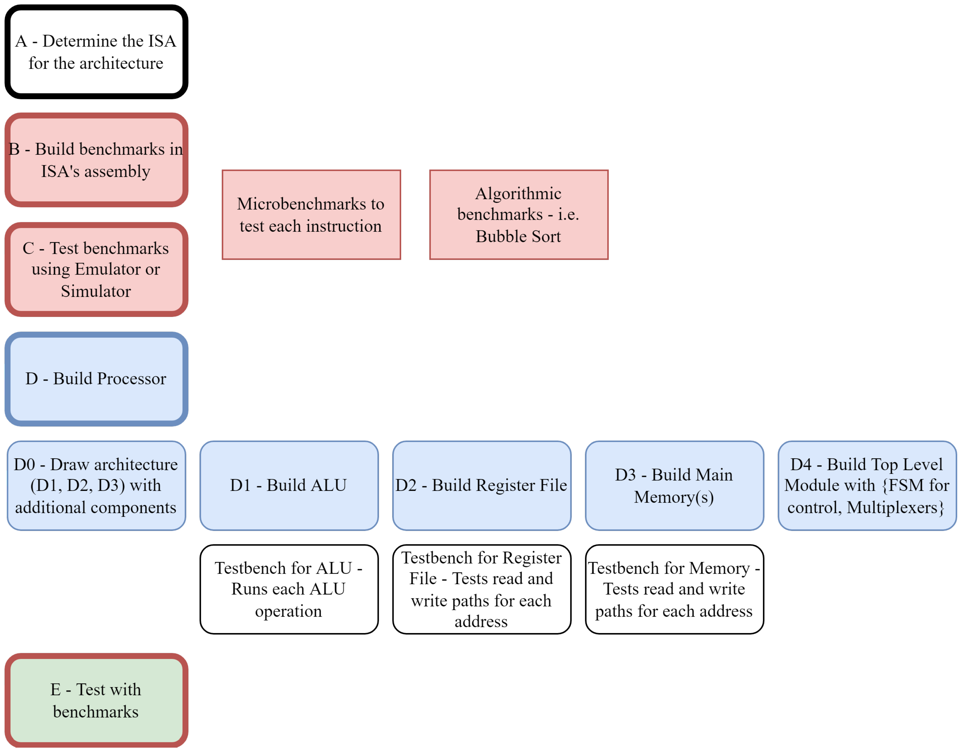
The overall activity follows the steps as shown in
Figure 1. We will reference the lettering in this diagram as they relate to the various steps.
In this section, we will cover:
Tools for creating and assembling benchmarks;
The specific FPGA tools and target FPGA;
Assumptions about the RISC-V architecture to make the design tractable;
Extensions that students have implemented to their base core RISC-V.
3.1. Simulator and Assembler for RISC-V Benchmarks
The most popular tools used to help understand an architecture are a simulator/emulator and an assembler. For example, our favorite tool for understanding MIPS-based architectures is the MARS [
12] emulator, which includes both the assembler and emulator together in one tool.
For RISC-V architectures, there is an ever growing set of tools available on the RISC-V site (
https://github.com/riscvarchive/riscv-software-list (accessed on 22 July 2022)). For our students, they either use Morten Petersen’s “Ripes” available at
github.com/mortbopet/Ripes or RARS available at
https://github.com/TheThirdOne/rars (accessed on 22 July 2022). Ripes is a simple tool that simulates a 5-stage pipelined RISC-V machine (not necessarily helpful for the actual design on the FPGA) and “Ripes” can easily generate machine code for a respective assembly program. Similarly, RARS is a version of MARS [
12], which is our favorite emulator tool for experiencing MIPS or RISC-V assembly programming. RARS provides compiled code and hexadecimal encoding of the RISC-V instructions after compilation.
Other SW tools such as a cross-compiler version of “gcc” and “gdb” are available to take high-level code and compile and debug the RISC-V architecture. These tools, though useful, are not necessary for the FPGA implementation and testing described for the first part of this work.
The above two assembler tools are used by students to create a set of two or three benchmarks that will exercise the RISC-V processor in testing (corresponds to
Figure 1 step B and C). Typically, we would expect these benchmarks to test each of the instructions available on the actual RISC-V processor including tests for basic C programming constructs such as “if”, “for”, and “while” statements and basic arithmetic and pointer statements. The culminating benchmark should be an implementation of a simple algorithm such as bubble sort.
3.2. FPGA Tools
The tools we use for our FPGA implementations of a RISC-V processor are all Intel based. Note, however, that any FPGA CAD flow can be used. Moreover, our HW implementation language is Verilog [
41], which is one of the common HDLs. This exercise can also be conducted in other HDLs, such as VHDL, in schematics, or in higher-level HW design languages such as High-Level Synthesis flows [
42]. We recommend using an HDL as a good compromise design approach for creating a processor as long as students have taken prerequisite digital design courses and have an understanding of what circuitry is described by their “synthesizable” HDL.
The Intel FPGA CAD flow is called, Quartus, and this flow synthesizes HDL designs for a targeted Intel FPGA. Miami’s labs have DE2-115 boards from Terasic, and these boards include a Cyclone FPGA. Quartus includes an FPGA programmer that allows the design to be synthesized and programmed to an FPGA on the prototyping board over a USB connection.
The Quartus tool can be set up to use ModelSim, which allows a student to simulate their digital design of the processor. For HW debugging, a tool called “SignalTap” allows the actual processor designer mapped to the FPGA to be analyzed where “SignalTap” is an on-chip logic analyzer. To debug digital designs, both simulation (via ModelSim) and the logic analyzer (via SignalTap) allows a student to observe system behavior. Also note, with the simulator alone, a student can complete most of this described exercise and demonstrate that their processor works without needing a physical FPGA (as was performed in the online COVID-19 year). When this course is taught in person, normally, we require that the processor design works on a real FPGA, which emphasizes other aspects of real digital system engineering including constraints such as the board’s clock frequency and limits of silicon area.
3.3. RISC-V Architecture Constraints
The RISC-V version 2.2 documentation has a frozen base ISA [
4] that has two variants—32-bit or 64-bit. For this work, we use the 32-bit RV32I as the base ISA. We further constrain this ISA by using Cornell’s Tiny RISC-V ISA (
www.csl.cornell.edu/courses/ece5745/handouts/ece5745-tinyrv-isa.txt (accessed on 22 July 2022)); the TinyRV2 described in this document is a simple processor that includes 34 instructions (corresponds to
Figure 1 step A) in the following instruction categories:
Control/Status Register Instructions;
Register-Register Arithmetic Instructions;
Register-Immediate Arithmetic Instructions;
Memory Instructions;
Unconditional Jump Instructions;
Conditional Branch Instructions.
The benefit of starting with this small ISA is students have a defined subset of the ISA that they can understand and implement, giving them a basic feel for how to design a computer.
3.4. Architecture Implementation Details
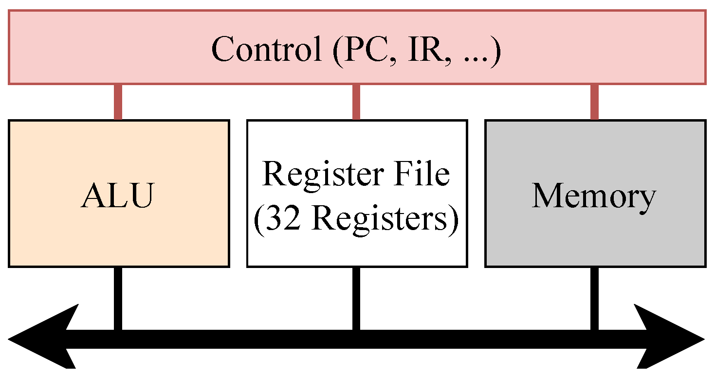
Figure 2 shows a simple block diagram of the four major components of most processors including the RISC-V processors designed here. In this section, we describe our methodology that allows students to create their architecture similar to these two images.
We recommend that a student follows the following design steps to create their version of a processor (corresponding to
Figure 1 step D0). First, we suggest that a student create their own block diagram that includes detailed control lines and HW components such as multiplexers (muxes), and additional registers such as the program counter (PC) and status register. There are two reasons for this. First, so the learner can demonstrate that they understand what the data path is in their architecture, including the control signals that will transport the data correctly for a given instruction. Second, this provides a useful high-level design that the teacher can examine to quickly assess if the learner understands their system design. For example, we suggest looking at a detailed architecture block diagram of a RISC-V processor in Patterson and Hennessy’s textbook [
27]. Note, however, the design depicted in their is designed as a single cycle processor with two memories for instruction and program data. Due to the realities of the Intel FPGAs available to our students, this architecture cannot be realized because of the on-chip memory (which has a minimum 2 cycle access). Therefore, each of the student’s processor is uniquely designed based on the following approach.
With the student’s diagram each of the major components, excluding the control, is created in HDL and can be tested independently (corresponding to
Figure 1 steps D1, D2, and D3). To achieve this, each component is implemented as a module in Verilog and tested with its own testbench. Generally, we recommend building these components in the order of arithmetic logic unit (ALU), the register file, and then the memory (a single memory for both program and data). A module’s inputs and outputs should correspond, directly, to signals in the designer’s initial diagram.
Instead of designing the memory module(s) directly in Verilog, we recommend that learners use Quartus’ “IP Catalog” tool that allows a designer to implement on-chip memory. The IP tool can create a memory using dialog menus, and as the memory is specified, it shows a schematic of the memory module including input and output signals. Using the IP tool, the designer can set up a memory initialization file (mif) that will read the data that the on-memory will be initialized with once the design is programmed onto the FPGA. Using the mif files, the designer can load their machine encoded assembly programs directly to the FPGAs memory, and for simplicity, we assume that all programs start at address 0 (PC = 0 × 00000000). More complex memories and bootloaders can be created for this system, such as off-chip SRAM memory chip available on the DE2-115, but to simplify the initial design, we use the on-chip, memory initialized approach. One key aspect of the on-chip memory IP is that it takes two clock cycles to load and store data, and this will need to be taken into account for when designing the control of instructions that read and write to memory including the fetching of the instruction.
The register file could also be created with the IP tool as simply a two read-port on-chip memory module. Instead, we recommend that students create a register file as a Verilog module that implements the registers as soft-logic on the FPGA, which includes sequential flip-flop bits. There are two reasons for this. First, the access time of the register file will be one clock cycle, which is more similar to a real ASIC design and this allows a demonstration of how a simple cache would improve performance of memory operations, and second, the design process of building a memory helps students understand the design of memories from both the write and read path.
When the ALU, memory, and register file are all created and tested, the final step is to integrate these components and design the control (corresponds to
Figure 1 step D4). Each of the three design components are integrated and instantiated in a top-level module that also contains a finite state machine (FSM) for the system control, mixing logic for some of the datapaths, and control signal generation from an instruction register to control the remainder of the processor. We assume that the architecture is a four-stage processor (fetch, decode, execute, and writeback) and this represents the starting model for the FSM. The exercise is to then determine the control signals needed at each stage of the FSM to move the data around, and this exercise is a function of understanding the control signals in the system and identifying which signals need to be set for each instruction. Branching and PC incrementing are the last part of the exercise that needs to be designed in the control during the writeback step.
3.5. Implementations and Extensions to the RISC-V Processors
Since 2019, five students chose to implement the RISC-V processor on an FPGA where some were completed during COVID-19 and in those cases, the students implemented a simulation of the processor as opposed to programming a real FPGA. All students who take this course have completed basic programming courses and have completed a second year digital systems course, which introduced them to either Verilog or VHDL. In each case, the above described tools were used to design the processors and map them to DE2-115 prototyping boards.
Table 1 provides basic information on the implementations. Column 1 shows the last name of the designer, column 2 shows the ISA, column 3 provides the URL to the code repository for the design files (if it exists; NA if it does not), and column 4 describes extensions to the architecture that students did to obtain an advanced badge in the course, where an NA means they did not pursue an advanced badge. Finally, all the processors created have no CSRR or CSRW instructions.
Extensions to the base HW can include extending the base system with a cache, pipelining, multicore system, or programming some operating system functionality [
43,
44,
45]. The extensions to the base processor include the following: McGrew implemented a simple cache and implemented the basics of an OS context switcher. The memory IP from Quartus takes two cycles to access the data from in load operations. The goal of the cache is to build HW to make loads only cost one cycle on cache hits. Both Schonauer and Qian implemented a multicore system with a fence for access to shared memory, where the multicore implementation demonstrates a simple shared memory parallel machine with two cores that uses an arbitrator to implement a fence synchronization operation.
3.6. Summary of Tools
We briefly summarize the SW and HW tools used by students to create their RISC-V processors and create the programs that run on their processors.
Table 2 presents a summary of the SW and HW tools used by the students to implement and test their designs. Note, that RARS is the preferred RISC-V emulator, as it also assembles the code into machine code that (with a few modifications) can be loaded into the internal FPGA memory as the benchmark programs.
4. Microcontroller Design on the FPGA for Arduino
Our next educational experience is the extension of a basic RISC-V processor to include microcontroller capabilities. In this section, we describe our experiences with one student group implementing these extensions.
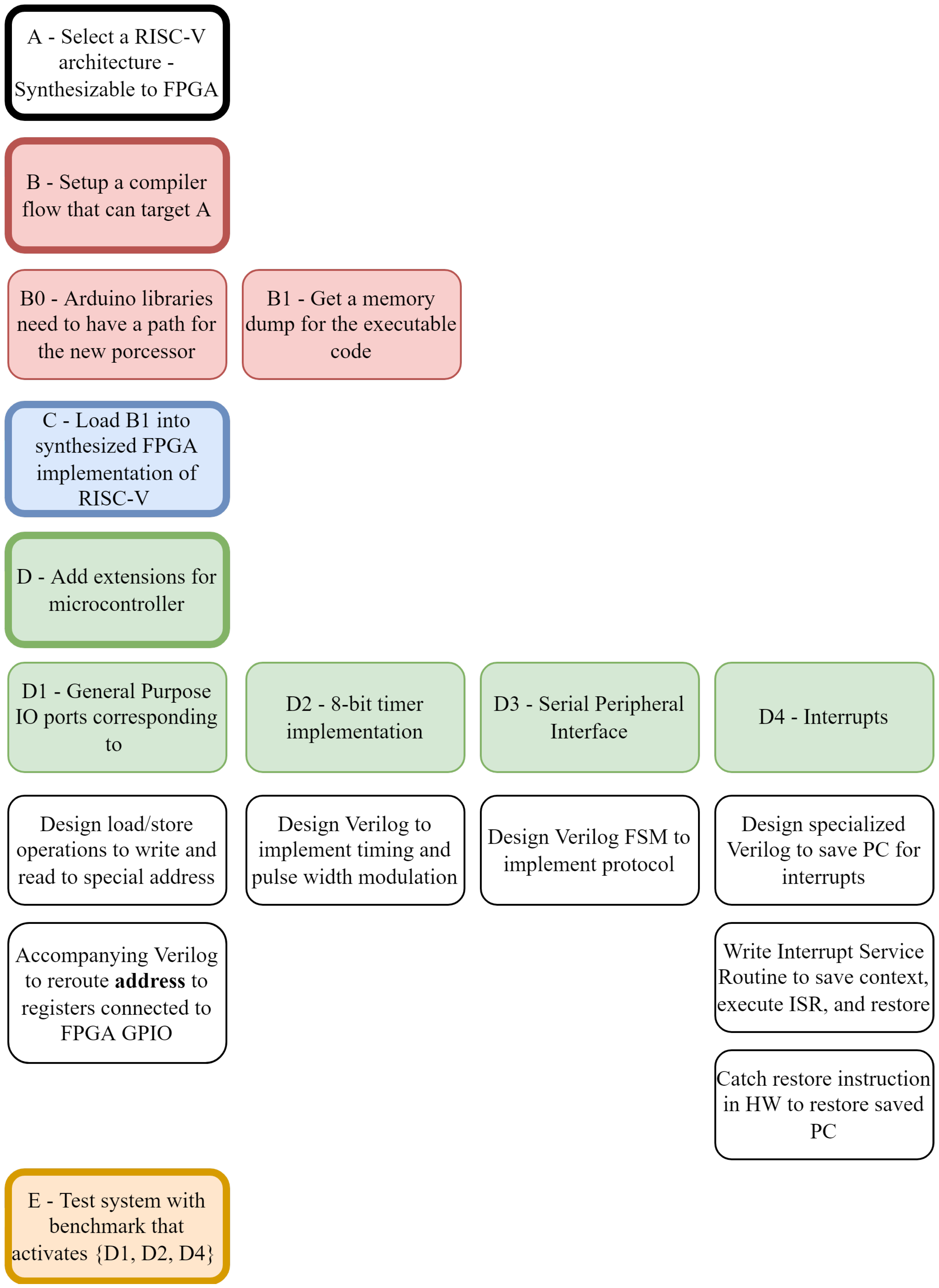
Figure 3 shows the tutorial steps followed to build the microcontroller and we will reference these boxes in the following text as it relates to the activity.
The two key design pieces for a microcontroller that can execute Arduino-like code is the implementation of the HW on an FPGA and the targeting compiler tool-flow. We will present each of these two aspects and provide a brief discussion in each section about what an undergraduate learns compared to just programming an embedded microcontroller.
Before looking at the choices and experience in designing the pieces of the microcontroller, we will first define some of our tools and starting points as these drive the final design.
As previously described, the FPGAs we have available for this work are the DE2-115 Terasic [
47] with an Intel Cyclone FPGA [
48]. To map HDL designs to this, we use the Quartus CAD flow, which is provided freely by Intel in the same process as above. Note that these tools and FPGAs can be substituted with any other flow.
Even though students have built RISC-V processors, we chose to start with a more mature RISC-V core called the Trireme Platform (corresponds to
Figure 3 step A). This RISC-V architecture is a single-core simple version of a RISC-V core derived from the work by Agrawal et al. [
49]. We note that this creates a disconnect between the two educational activities as the students are not using their own RISC-V processors in the second experience. However, the complexities of real compilation flows would require that in the creation of their RISC-V processors, significantly more details must be considered and a larger ISA is implemented. For this reason, we believe that instead of spending undergraduate time on implementing low-level details, we start with an existing RISC-V processor that works with a real compilation flow.
4.1. Tool-Flow and Software
The tool-flow to target the microprocessor consists of two overarching steps:
We will briefly describe both stages.
4.1.1. RISC-V Compilation for Arduino Behavior
As our goal is to have our microprocessor be targetable, such as an Arduino UNO, our first focus is on compiling the embedded system C code with support for common Arduino libraries (corresponds to
Figure 3 step B0). To update the Arduino libraries to target our RISC-V implementation means that the Arduino libraries are updated with C “#define” statements to support HW-specific processes for the RISC-V processor. For example, the function call “void _delay_ms (double __ms)” available in the “util/delay.h” header file for AVR microprocessors needs to be defined for the RISC-V processor at our clock frequency rate (50 MHz). Similarly, the “arduino/io.h” needs to be extended to include our RISC-V version with the appropriate port mappings.
With proper library implementations, the next key step is how to run the compiler flow and create the memory dump of the executable compiled code that will be loaded onto the FPGA (corresponds to
Figure 3 step B1). Trireme uses a standard RISC-V GNU toolchain with Newlib, and this needs to be installed onto a Linux distribution. Similar to the Arduino UNO microprocessor, the Trireme processor is a bare-metal microprocessor and the compilation needs to create an executable that specifies aspects of the actual processor address space including RAM size and stacksize, and the compiler outputs a Verilog Memory Hex (VMH) file that can then be processed to initialize the processor in either simulation with ModelSim or can be mapped into on-chip memories available on the FPGA. This VMH file represents the executable code (machine code) for the microcontroller.
4.1.2. FPGA Implementation and Execution
Once the embedded C code is compiled into a VMH file, the next step of the tool-flow is to load the program into an FPGAs on-chip memory, and either run or simulate the system (corresponds to
Figure 3 step C). For the sake of brevity, we will skip over many of the details for simulation of the microprocessor and will focus on the actual implementation on the FPGA, but note both flows are possible. In the case of simulation in ModelSim, the testbench needs to simulate input timing signals for aspects such as external interrupt signals and serial communication.
Trireme’s approach to dealing with byte-addressable word-aligned memory writes and reads in RISC-V is to split the memory across four individual RAM IP modules, each with 1-byte of a 4-byte word. Therefore, the first thing that must be conducted is to split the VMH file, which contains all the data for the executable program, written in words into four separate memory initialization files (splitting the word into 4 bytes). We wrote a Python script that automates this process and creates four different byte initialization memory files from the compiled VMH file.
Next, to execute the RISC-V microprocessor, the Quartus synthesis flow is invoked in Quartus and the resulting design is programmed to the FPGA, which includes the above memory initialization. Once the reset signal is sent, the microprocessor will execute the embedded system program at a specified starting address.
Additional tools are used for debugging the processor including SignalTap, which allows the FPGA to be observed as if it was connected to a logic analyzer. This tool is very useful in observing internal signals, registers, and control of the processor and is facilitated by bringing signals out through the top-level definition and instantiating SignalTap.
4.1.3. What Is the Importance of the Tool-Flow and Library Code?
Understanding and experiencing tool-flows is a fundamental skill in undergraduate CpE education. In many ways, being shown one IDE and tool-flow is detrimental to a student as they begin to assume tool-flows are magic, and usually, the early IDEs that are adopted in education are commercially mature tool-flows with millions of users. Examples of these flows include Eclipse for early programming, Arduino IDE for simple electronic control, and Matlab or Mathematica for numerical programming. The large user base for these IDEs means that these tools have been significantly revised and improved, which is not true for more experimental or smaller user base tool-flows that students will, likely, experience in their future careers. Additionally, for many undergraduates working with C libraries and updating them for a different architecture might be their only experience in working with the link between SW and HW, and these experiences will help them understand some aspects of HW/SW Co-Design.
Our approach to using the Arduino IDE at our university is to allow the IDE to be treated as a magical black box in early first and second year courses, but once a student reaches our course in embedded systems (in the third or fourth year), we begin to remove the magic and ask students to treat the AVR processor (ATmega328P [
50]) as a microcontroller that can be programmed in C and compiled for directly with a command line using the programs “avr-gcc”, “avr-objcopy”, and “avrdude” to compile, create an executable file, and finally, load the program to the ATmega328P with its bootloader.
Similarly, the tool-flow used for the bare-metal Trireme microprocessor system teaches students the complexity of tool-flows that are not heavily supported. Additionally, this process provides students with a deeper knowledge of Linux, and how to use the command line to install packages and get a tool-flow running. Students now can begin to explore questions such as:
How does an executable file get created and loaded into a processor’s memory?
What are bootloaders, and why do they help make systems easier to use?
How does a processor know where the different parts of a program goes in memory?
What is the file format for an executable of a program, and why are is this format needed?
Why is the open-source world of Linux so powerful?
4.2. Hardware Extensions of the RISC-V Microcontroller
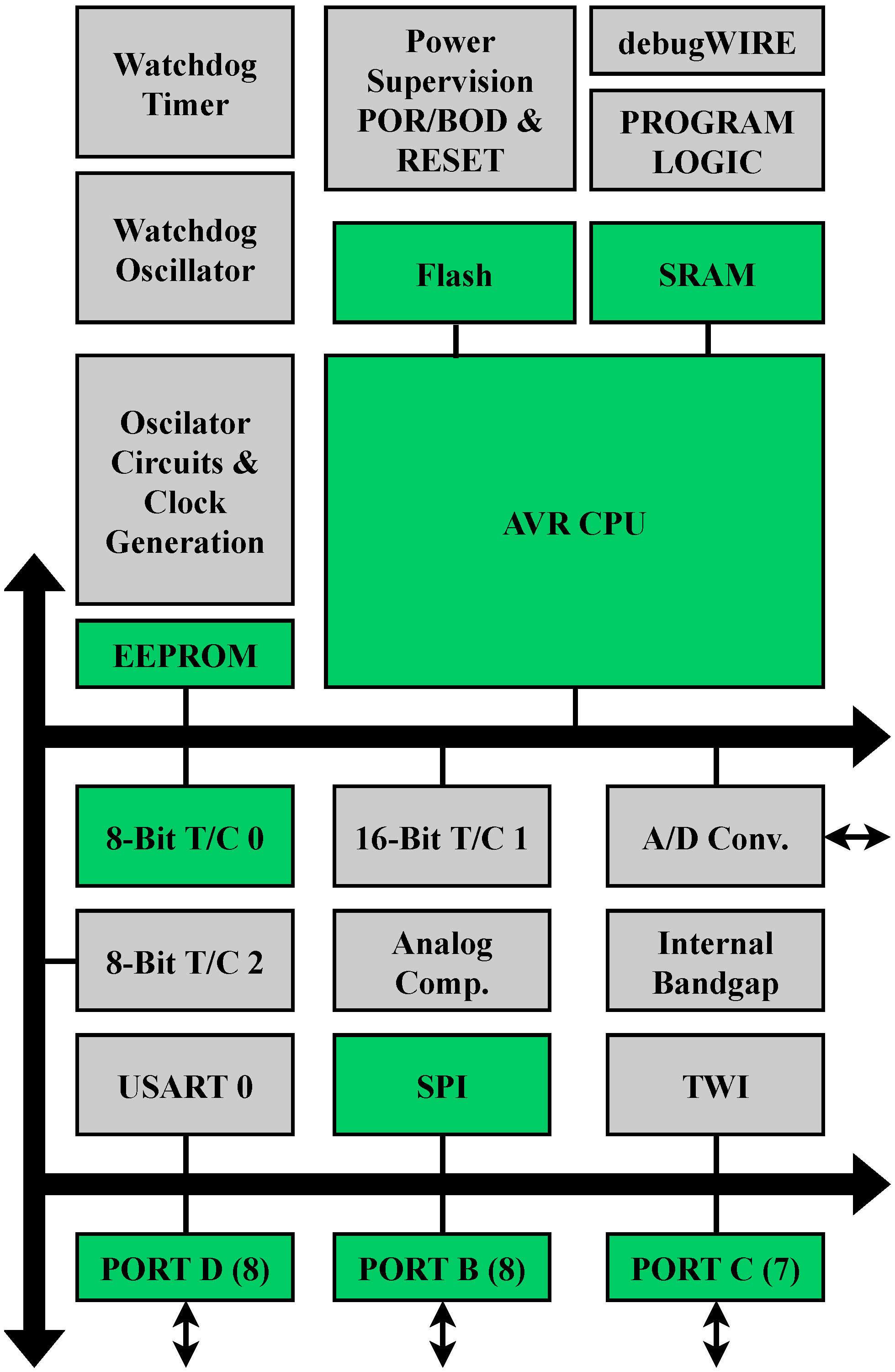
Figure 4 shows the block diagram of the ATmega328P [
50] microcontroller. In green, we show the blocks of the system that have been implemented in our design, and the blocks in grey are not implemented. Note the large AVR CPU box in the center is implemented as the RISC-V Trireme processor noted above. All of the other pieces of the design are implemented as individual pieces of HW designed in Verilog. However, the SRAM, Flash and EEPROM are just implemented as on-chip FPGA memory and are simple volatile memories.
We will briefly describe the HW (and related SW) designed for each of these green boxes, which include:
The input and output ports;
The 8-bit timer with Pulse-Width Modulation (PWM);
The Serial Peripheral Interface (SPI);
Subset of interrupts and interrupt service routine.
4.2.1. General Input/Output Ports
Ports B, C, and D are shown at the bottom of
Figure 4 (corresponds to
Figure 3 step D1). These general purpose digital I/O ports are used to control the pins of the microcontroller as either inputs or outputs and are controlled via three registers for each respective port. There is a data direction register, a port control register, and a pin register where the first two control how the pin register (on a per bit control) is used as either a read register or write register.
From the perspective of the RISC-V microprocessor, these three registers are treated as special addresses in the address space of the processor. Therefore, a standard store or load assembly operation is written in the embedded C code to access these registers. From a HW standpoint, we define these ports to have specific addresses in the address space, and we redesign the load and store instructions to these specific addresses to have specialized functionality when addressed by implementing multiplexed paths that allow these registers to be read and written from. This modification allows us to implement specialized I/O behavior for the pins with the exception of allowing the microcontroller to change the pin direction during execution time.
The reason we do not implement the full bi-directional functionality of the I/O pins is due to the complexities of the FPGA and implementing this with the Verilog “INOUT” ports. Instead, our solution is to force the microcontroller to select if the pin will be an input or output port at synthesis time and programming the GPIO of the FPGA in the chosen direction.
4.2.2. 8-Bit Timer with PWM
The 8-bit timer, as described in the ATmega328P documentation [
50] in chapter 15 is attached to Port B and has a number of features such as a comparator, PWM, and can drive an interrupts for the processor (corresponds to
Figure 3 step D2).
We implemented the 8-bit Timer counter-0 in Verilog using all the same names as appears in the ATmega documentation, and our implementation includes all the features available for the timer including PWM at a specified duty cycle. As there is no specialized digital HW, such as tristate buffers, this HW can be replicated exactly the same as how it operates on the ATmega328P in a Verilog module on the FPGA. We did not implement the second 8-bit timer or the 16-bit timer as this exercise is mainly copying the first timer and adding a few minor features to accommodate each of the timers’ slightly different capabilities. Registers of the timer are included in the address space so they can be accessed by the SW, in the same way, as we added the port registers.
4.2.3. Serial Peripheral Interface
Similar to the 8-bit timer, we also implemented a full Verilog version of the SPI HW module as described in chapter 19 of the ATmega328P documentation (corresponds to
Figure 3 step D3). This HW is a simple four-pin communication protocol, and the microcontroller can be put in either parent/master or child/slave mode with slightly different operations in each of the two modes. Depending on the mode, the HW follows the respective Finite State Machine to control the protocol operation and the appropriate registers are mapped into the address space.
4.2.4. Interrupts
The last piece of our microcontroller design is the implementation of interrupts that can be handled by interrupt service routines in the embedded SW (corresponds to
Figure 3 step D4). The complete ATmega328P interrupt vector table is described in 12.4 of the documentation, and for our implementation, we only implement a small subset of these vectors to demonstrate the idea.
From the interrupt service routine (ISR) SW standpoint, the main job of the ISR is to save existing context of the currently running program (save all registers onto the stack including the return address), then perform the service routine for the interrupt, restore context (restore all registers off the stack including the return address), and then send a special instruction to return from the ISR. Note, in our implementation we do not allow multiple interrupts to happen to simplify our implementation.
From a HW perspective, our interrupts are implemented in Verilog via an FSM that starts in a “wait for interrupt” state. In this state, the interrupts that have been turned on are checked for constantly via a comparator that checks for each of the signal conditions.
When a signal trigger is detected, then the FSM proceeds to “SAVE the PC” state to save the current PC of the running program, and the program is paused from continuing. This PC value is saved in a special interrupt-saved PC register, as the return address register can not be used as it may contain an important value with respect to the currently running embedded system code. Next, the PC is updated with the address of the ISR that needs to be run, and the program (or ISR) is allowed to continue execution on the processor. Finally, when a special return from ISR instruction is detected (note, we use “andi 0, 0, 0”) we restore the PC with the saved interrupted PC and restore the program execution, moving into the original “wait for interrupt” state in the FSM.
This implementation of interrupts is a deviation from how the RISC-V processor and its’ ISA was created to handle interrupts, but from an undergraduate perspective, this approach works well enough to implement the interrupt feature in both SW and HW.
4.2.5. What Is the Importance of Implementing the HW Design?
From an undergraduate CpE student perspective, the interesting ideas that are learnt in this process is how additional HW can be designed around the processor to alleviate the SW from having to perform all the actions of an embedded system. This additional functionality, however, comes with challenges of how to be integrated with the ISA.
Of key importance is the idea of the address space of the processor, and how the HW can be designed to allow specialized registers to be accessed with a simple extension to the memory path of the processor basically by using multiplexers to drive different data-paths depending on a chosen memory address.
Additionally, students have the opportunity to see how standard FSMs and counters can be used to implement simple communication protocols and timers. By implementing these functionalities in HW, the processors’ capabilities are greatly enhanced with the parallel capabilities only realizable in HW.
Finally, the idea of what an interrupt is and how it can be implemented with HW provides a student with a much deeper understanding of the benefit of saving and restoring system context. This knowledge can be easily leveraged to then help a student understand how the process switching aspect in an operating system can be implemented with a few simple HW constructs.
4.3. Demonstration of the Microcontroller
The students have an online repository at
https://github.com/qiany21/Arduino-on-RISC-V (accessed on 22 July 2022), noting that the project was not intended to be used by others, and, is, therefore, poorly documented and organized (corresponds to
Figure 3 step E). However, we provide the design there for others if interested.
Our main demonstration of the work was to get embedded C code running on the RISC-V microcontroller with code that would match the behavior of a design implemented on an Arduino UNO. Our demonstration for both platforms has [A] one light (LED) blinking on and off at a set rate. Additionally, another [B] light (LED) is set to maximum brightness and on. Then, [C] when a button is pressed then [D] the brightness of the second light is dimmed until it is completely off (the next press after off will set it back to full brightness).
The above demonstration includes activation of the following HW and SW on either platform noted by the associated letter:
The input and output ports—[A], [B], and [C];
The 8-bit timer with Pulse-Width Modulation (PWM)—[B] and [D];
Subset of interrupts and interrupt service routine—[C].
Note, we tested the SPI in simulation but did not include it in our final demonstration.
We implemented this on both the FPGA implementation of our RISC-V microcontroller and on the Arduino UNO to show how the two are equivalent systems.
4.4. Summary of Tools
We briefly summarize the tools, both HW and SW, used for the creation of our RISC-V microcontroller.
Table 3 presents a summary of the SW and HW tools used by the students to implement and test their design. All of these tools are freely available.
5. CpE Curriculum for RISC-V Architecture and Microcontroller Design
The question after describing our two experiences with implementing RISC-V processors and a RISC-V microcontroller and all the peripheral tool-flows is “how should these activities” be integrated into CpE undergraduate curriculum, if at all?” To do this, we will first ask what is the goal of the CpE curriculum, and then second, we will formulate a few learning objectives from our exercises that could be generally tied to the CpE undergraduate curriculum. Our learning objectives will be written using Bloom’s Taxonomy Verbs [
51].
To determine how important a learning objective is, we suggest classifying them in the three categories provided by Wiggins and McTighe’s filter for learning objectives [
52] into three categories of deepening importance:
- 1.
Worth being familiar with;
- 2.
Important to know and do;
- 3.
Enduring understanding.
This filter allows a teacher to consider their learning objectives and qualify how important it is. As it relates to this work, we argue that the time spent on this activity for a learning objective needs to be in category 3 to make the process of value to the standard CpE curriculum.
Next, we ask what is a computer engineering curriculum, and for this, we take a passage from CE2016 [
1]:
An important initial aspect of the engineering ethos relates to acquiring the background necessary to understand and reason about engineering concepts and artifacts. This background stems from fundamental ideas in areas such as computing, electronics, mathematics, and physics. An important role of the body of knowledge for computer engineering is to expose and develop these fundamental notions. In many ways, the core of the body of knowledge reflects a careful set of decisions about the selection of material that fulfills this role. This basic material then provides an underpinning for additional material whose ultimate expression is the building of better or novel computer-based systems. A blend of theory and practice, with theory guiding practice, appears to be the best approach to the discipline. The curriculum should accompany this blend with attention to a set of professional, ethical, and legal concerns that guide the activities and attitudes of the well-educated computer engineer. The curriculum should also foster familiarity with a considerable range of diverse applications.
Therefore, the CpE guiding document does not specify which aspects of the curriculum should be deeply explored; the document suggests a “MUST” need for digital system design and embedded systems labs and a “Supplemental” for computer architecture labs, but this is in the space of designing some digital circuits, using microcontrollers as opposed to designing processors and microcontrollers.
We state the following learning objectives from our above activities where the Bloom verb is in boldface and comes at the fifth level Synthesis (of six levels):
Build a simple computer architecture and show that this system can execute basic assembly benchmarks.
Establish the tool-flow to compile embedded C code and program that code to a microcontroller.
Construct an address space and the accompanying modules such that the address of a load or store in the processor can be redirected to a custom hardware component.
Design an interrupt controller unit that detects a changed input signal such that the processor is stopped, the current PC is saved, and software for the ISR is executed to save context, execute, and restore context after the ISR.
Design the hardware to implement either an 8-bit timer or protocol to handle a simple two- or three-wire serial communication protocol.
If we look at an undergraduate curriculum, we would argue that learning outcomes 1, 3 and 4 from the list above, likely, fit under a filter categorization of 2 or possibly even of 1. Learning objective 5 sits in filter category 3 and is, likely, covered in some detail in Digital System Design courses (CE-DIG-8 Control and datapath design). Finally, learning objective 2 is covered in a number of spaces in the curriculum, and this would be considered an additional activity in that space that overall is classified in category 3 (but as this is not the only time this should happen, the specified activities above are, arguably, not necessary).
In the case of learning objectives 1, 3 and 4, the verbs Build, Design and Construct likely are treated at a lower Bloom level as either Application or Analysis. In this case, the student would have a more shallow understanding of the concepts but should be able to describe the ideas. This is, likely, where current CpE curriculum treats these ideas.
This brings the philosophical question back, of whether a computer engineer should design a computer in their education. For many of us, it seems unfathomable to not learn about a computer and then want to build it. Yet, for others, computer engineering is beyond the computer as a machine that is designed, and instead, is in a larger space, in which the computer and computing is leveraged for various CpE applications to other problems. Additionally, we all sit at certain abstraction levels in our understanding of where magic begins and where our deep understanding of systems begins. For some CpEs, the magic is not the computer architecture or the microcontroller, but sits at how a transistor or logic gate works. For others, the computation substrate, whether it be an FPGA, a microcontroller, a CPU, or a GPU is simply a device that allows us to run our algorithms. The breadth of abstraction levels for CpEs means it is difficult to determine what an undergraduate should experience.
6. Conclusions
In this work, we describe two CpE educational experiences in building RISC-V processors and the experience of undergraduates taking a RISC-V core and setting up the tool-flow and additional HW to implement many of the aspects of a microcontroller. For all of these students, the experience was both rewarding and challenging and most of them have continued into interesting industrial careers or graduate school in related areas. As these activities are student chosen, we have no conclusive data to the impact of these activities, but we note that of the students that chose the above activities, three out of six of these students have gone into graduate studies in related fields.
From our experiences, we then examine how these experiences relate to learning outcomes, and ask the question how important are these learning objectives in a CpE undergraduate curriculum. From our discussion, we would argue that having every undergraduate perform these exercises is, likely, too focused for the students without providing them broad educational experiences. If anything, this suggests that when appropriate, self-directed learning along the lines of badge-based mastery type learning can allow those with interests in these spaces to pursue them while allowing others to pursue other related CpE projects.
Still, it might be better to look at a device such as the XLR8 prototyping board, build a set of learning objectives from the CE2016 curriculum and then design a set of exercises and projects that could incorporate the XLR8 as the main device in teaching: CE-CAO Computer Architecture and Organization (60 h), CE-DIG Digital Design (50 h), CE-ESY Embedded Systems (40 h), CE-SPE Systems and Project Engineering (35 h), and CE-SRM Systems Resource Management (20 h) in a holistic low-level approach. We believe this would be similar to the approach taken by Nisan and Schocken [
9] to create a full flow for a student to experience from a low-level design approach. In this attempt, we suggest that the RISC-V is an excellent choice of a microprocessor for these exercises, as we have demonstrated. This will be even more true because many tools are becoming available to implement the core and the SW tool-flow reasonably quickly. Additionally, a bare-metal system such as Trireme would allow all of the next aspects of a computer system to be observed by the student including the creation of a simple operating system. From this, point aspects of networking, cybersecurity, and algorithmic execution could be further added onto this system, resulting in an affordable and deep CpE educational experience.


 ,
, 


