
A Tree-Based Architecture for High-Performance Ultra-Low-Voltage Amplifiers

 ,
,  , , and
Abstract
:1. Introduction
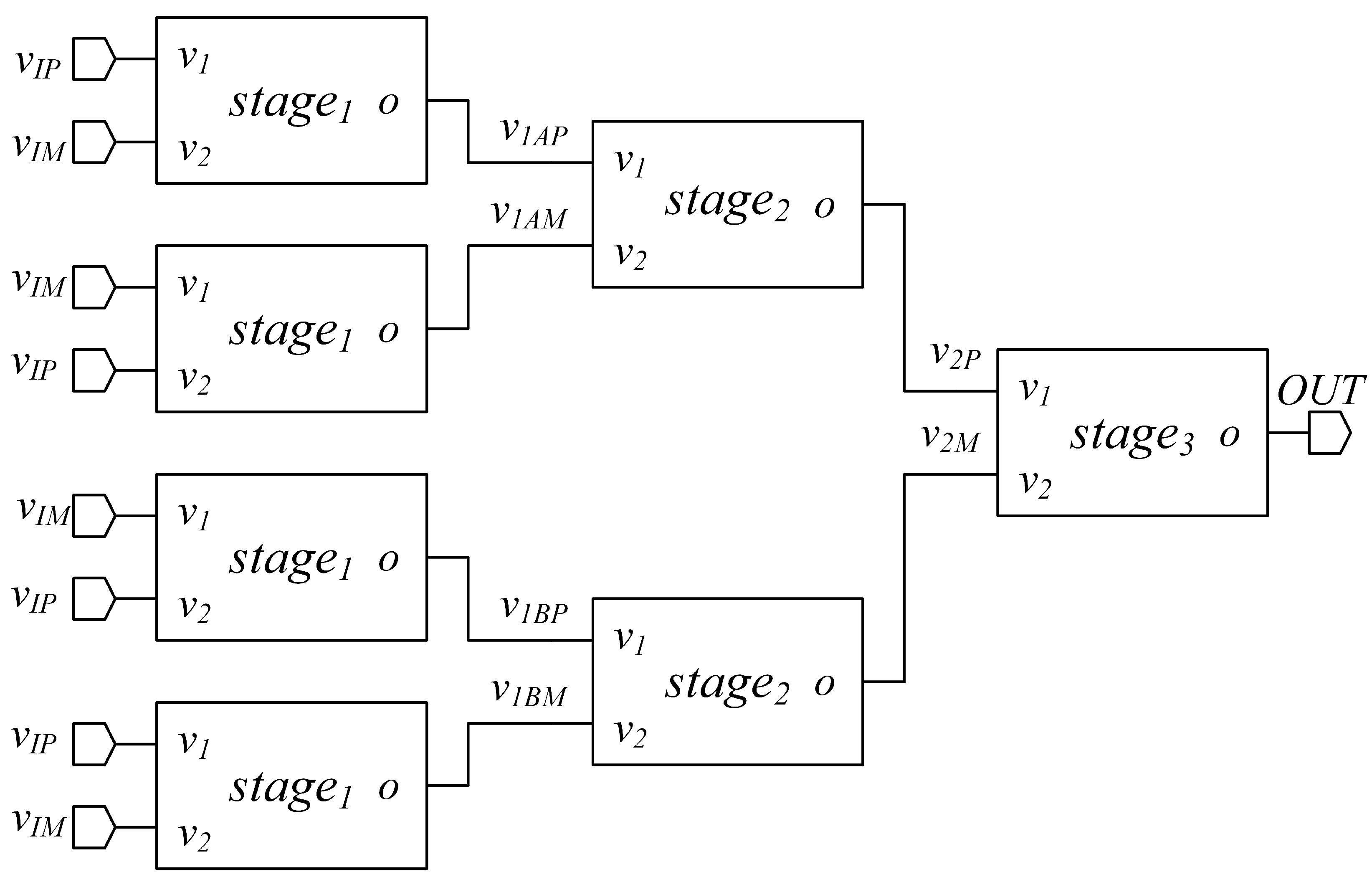
2. Proposed Topology
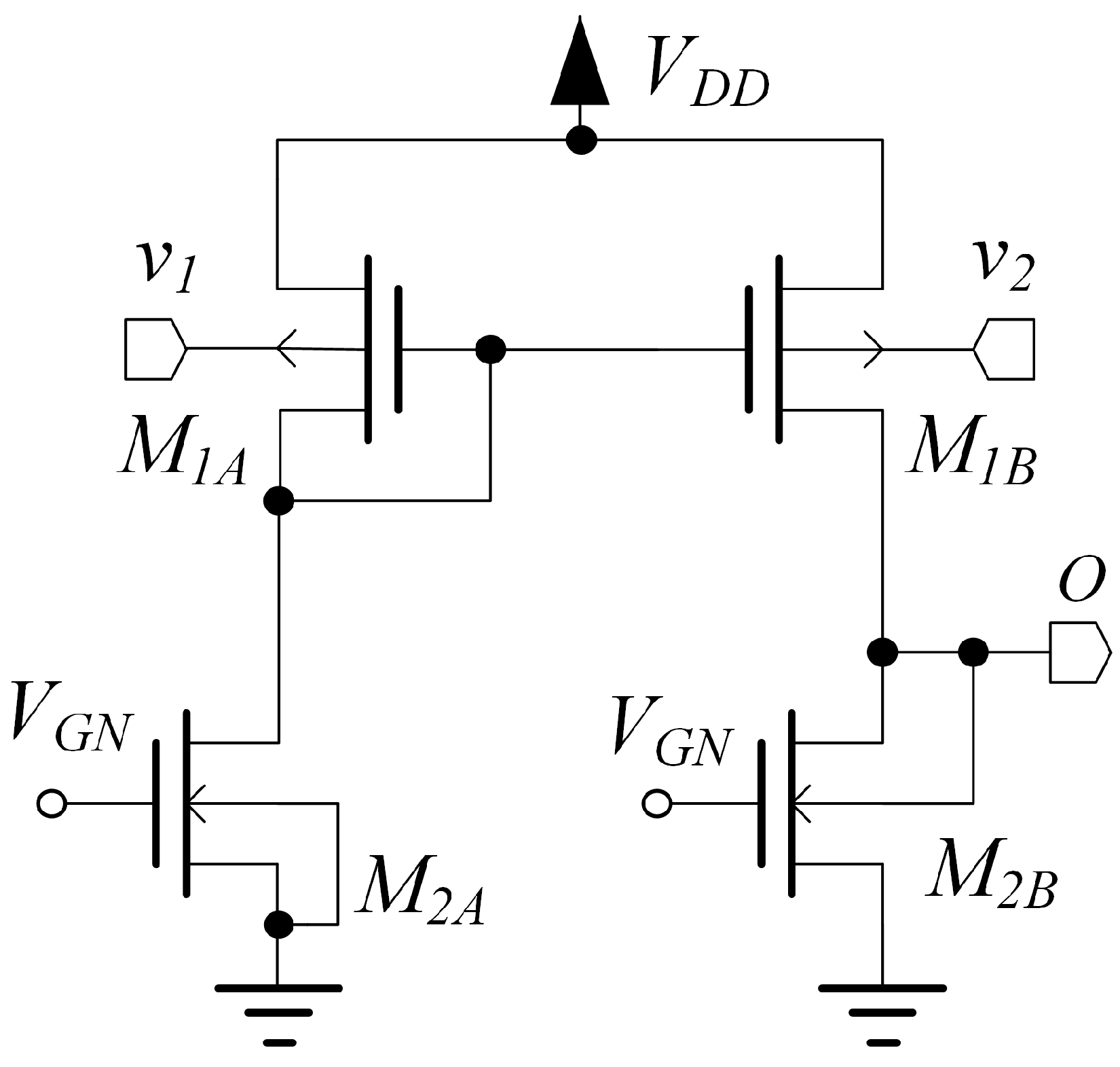
2.1. Stage
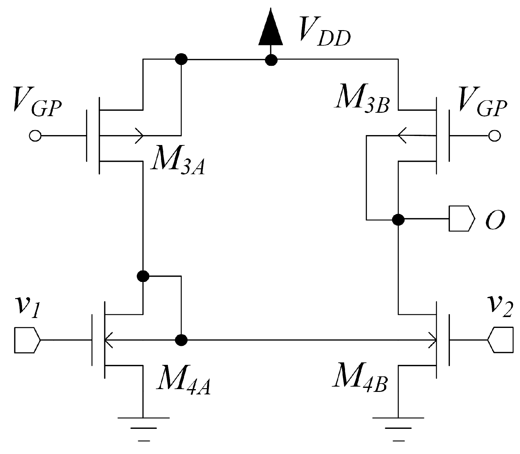
2.2. Stage
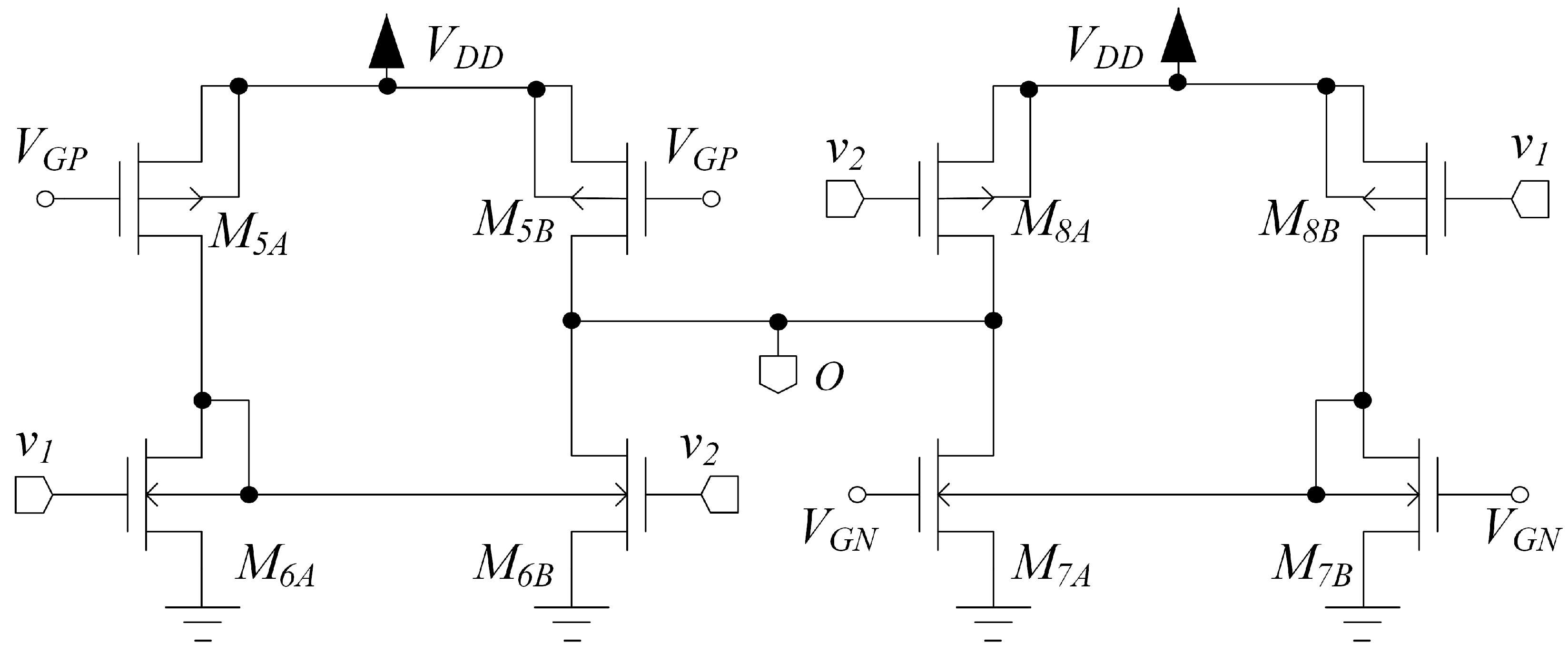
2.3. Stage
2.4. Architectural Considerations
3. Circuit Analysis
3.1. Differential Gain
3.2. Common Mode Gain
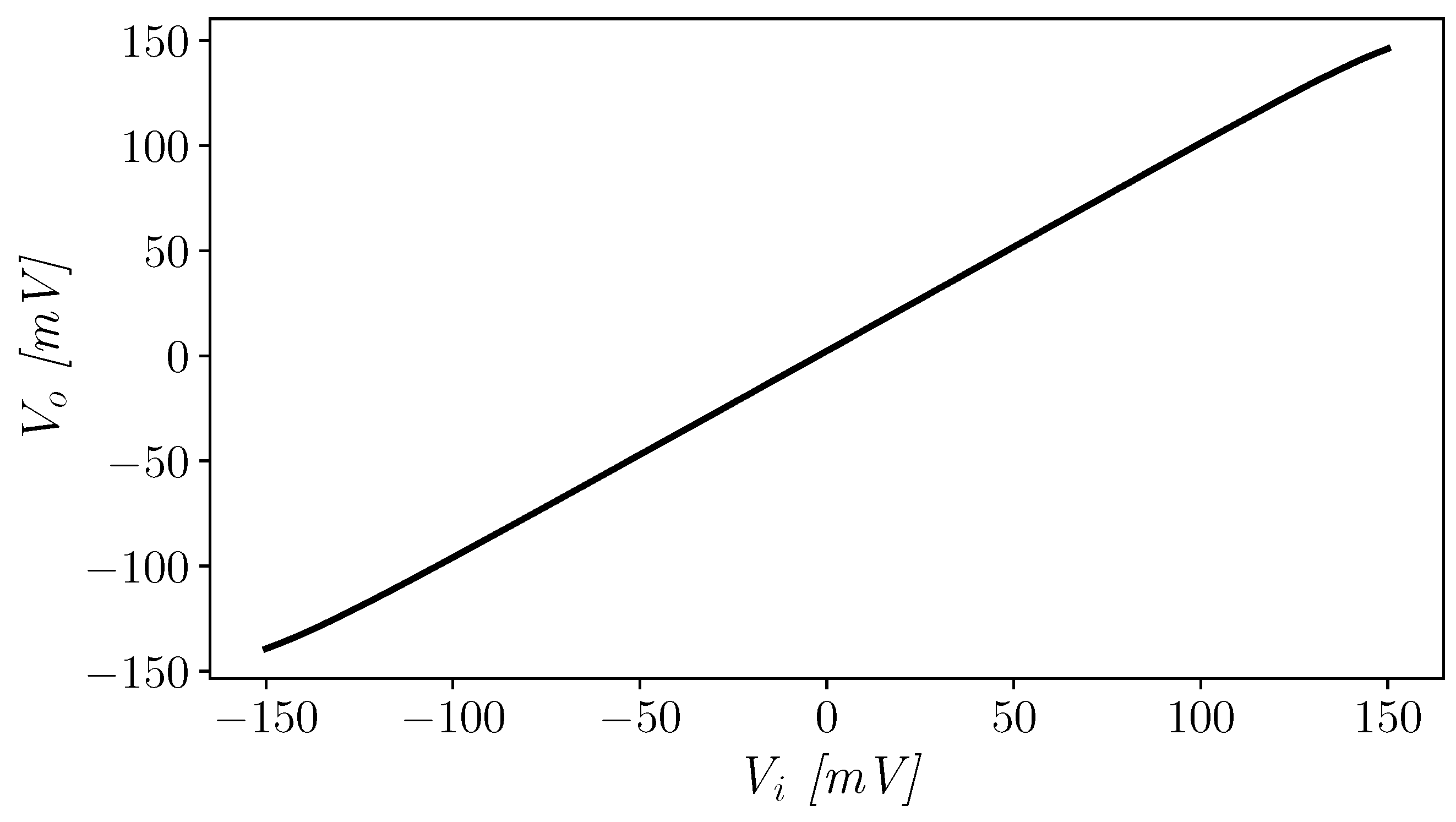
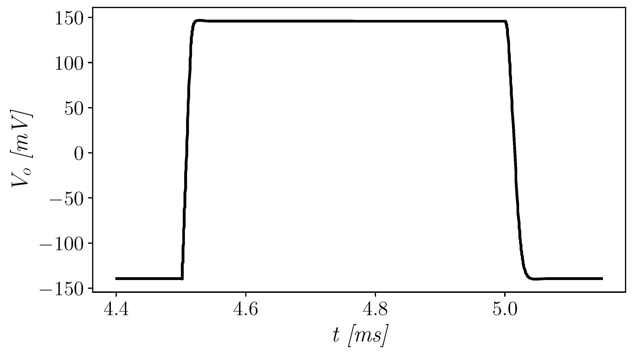
3.3. Large-Signal Performances
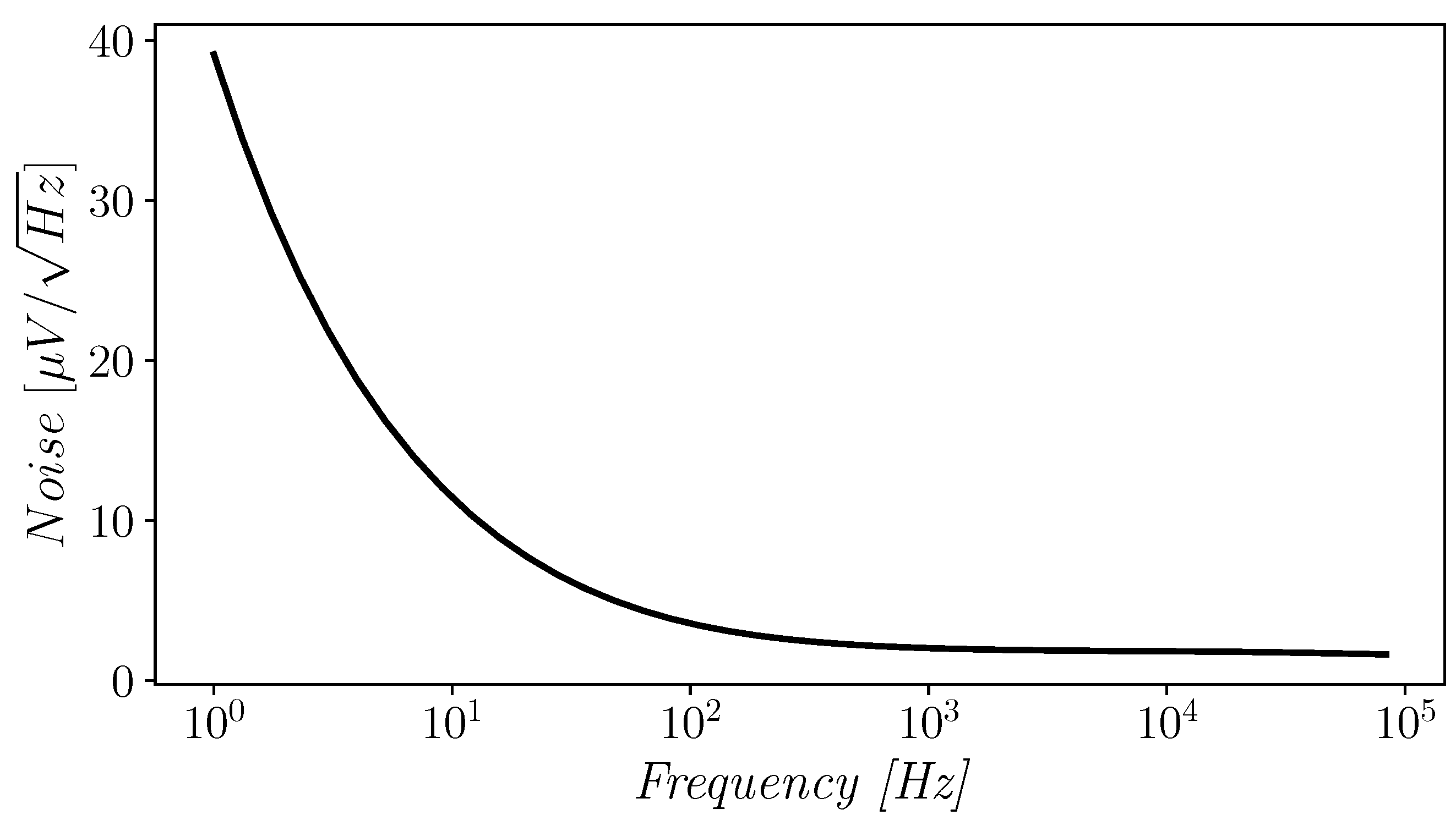
3.4. Noise Analysis
4. Amplifier Design and Simulation Results
4.1. Sizing
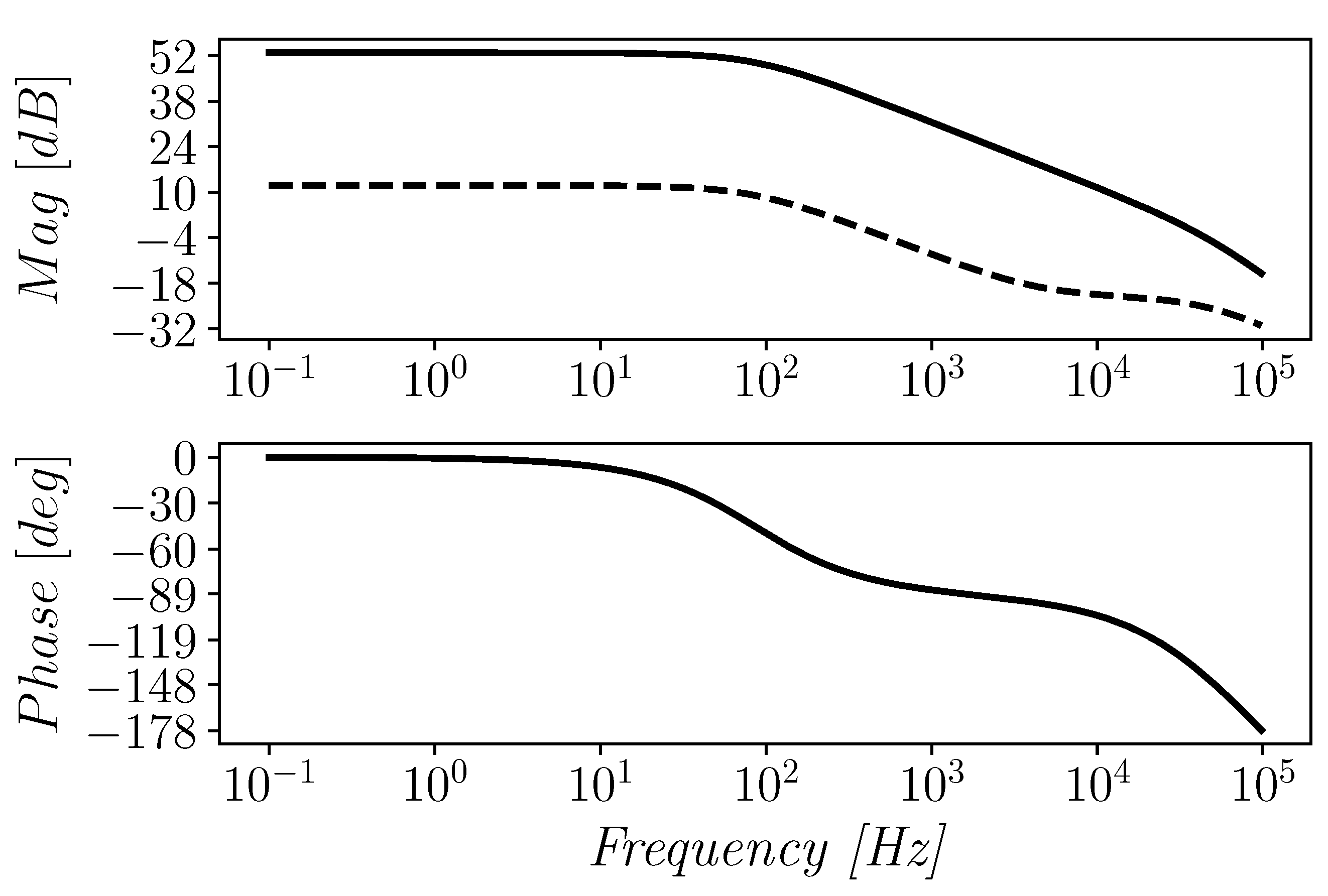
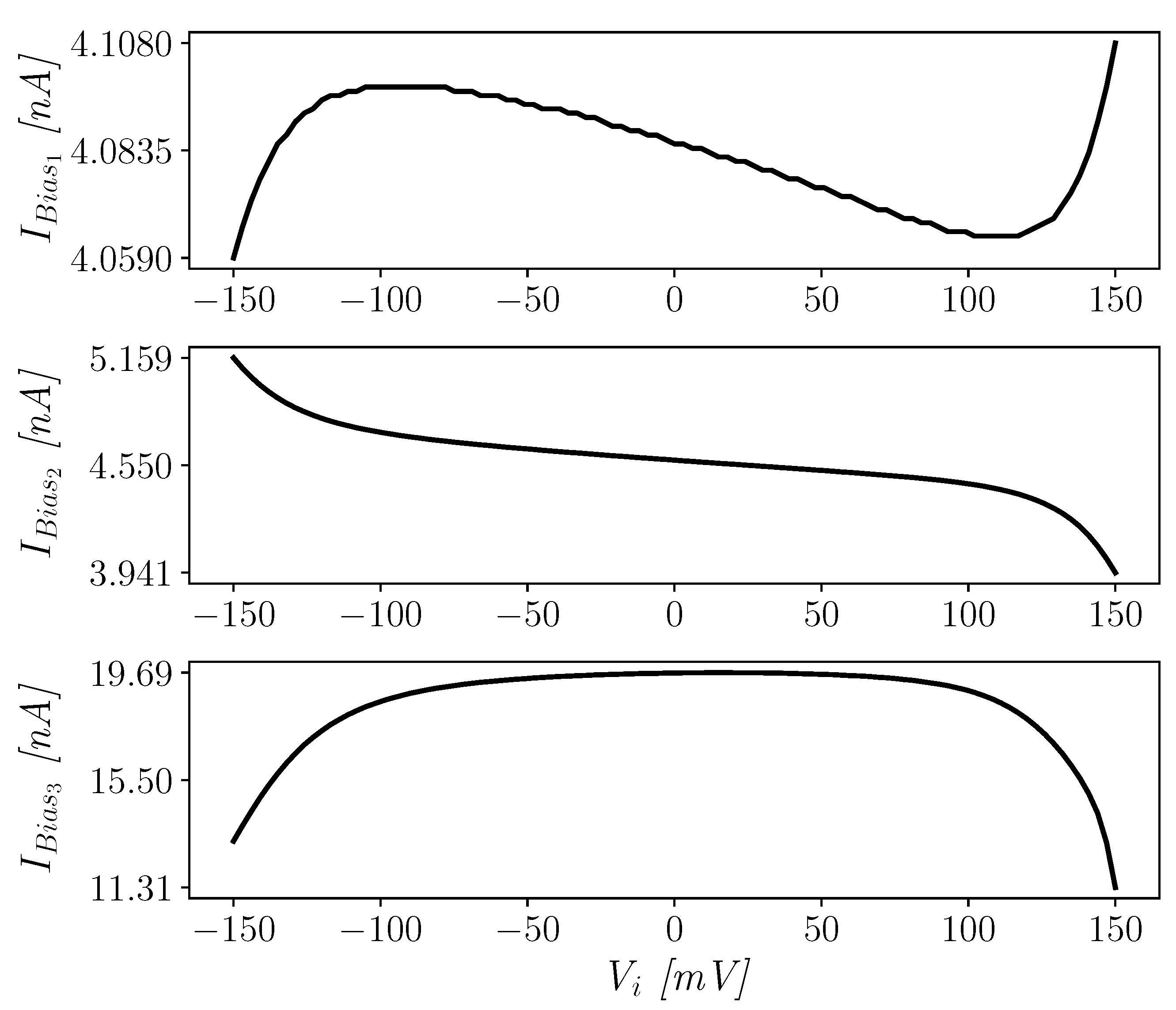
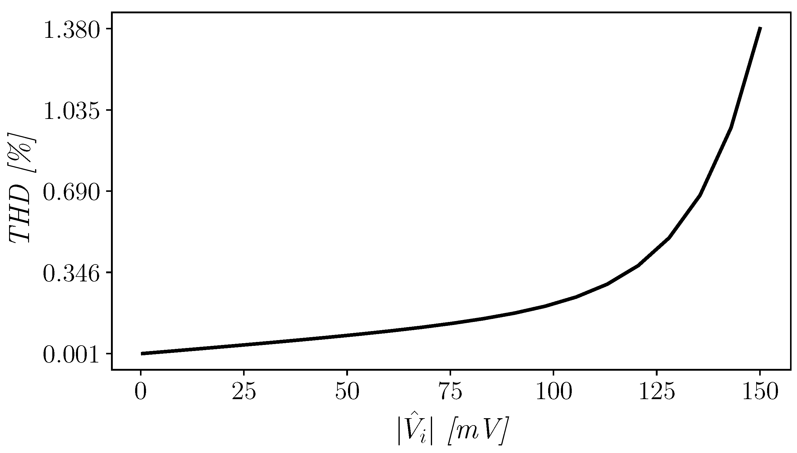
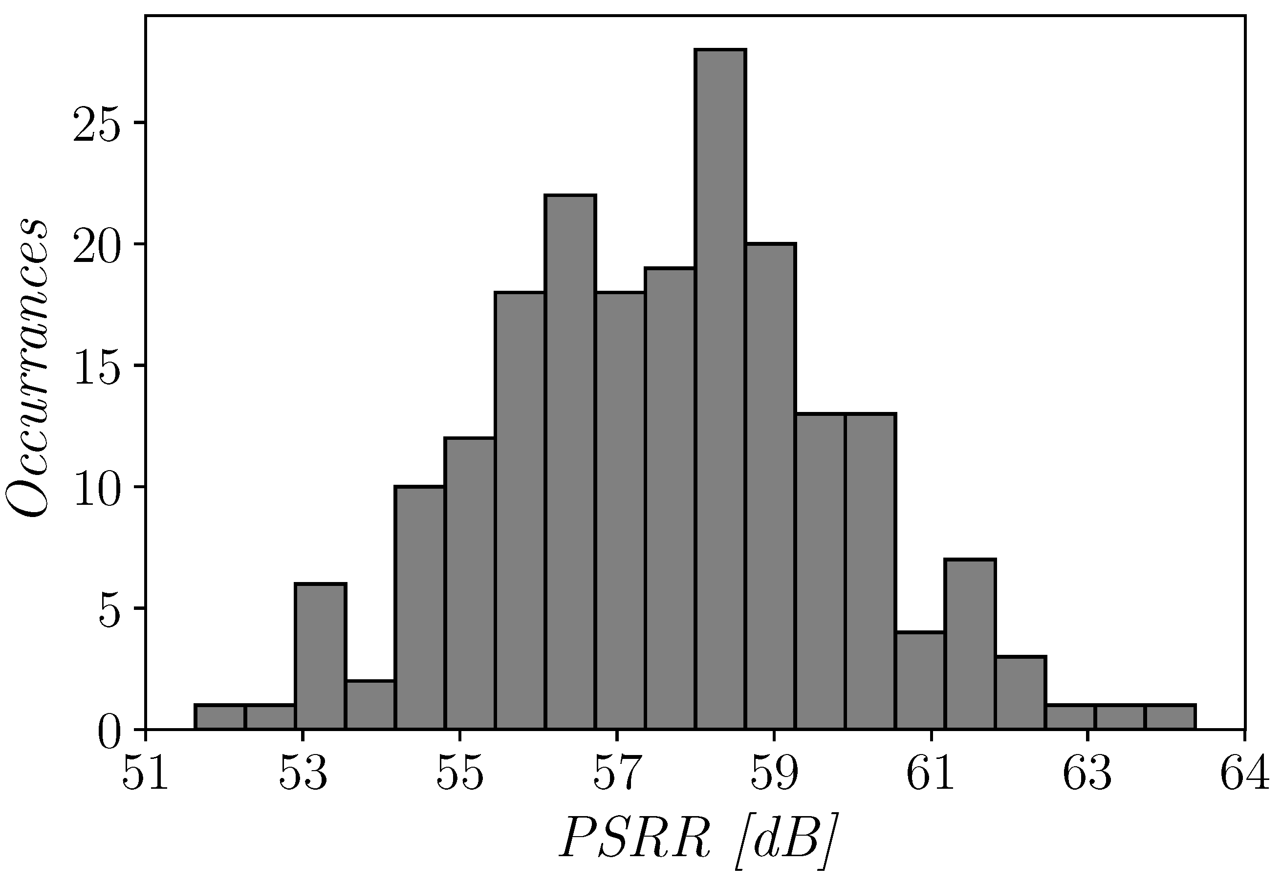
4.2. Circuit Simulations
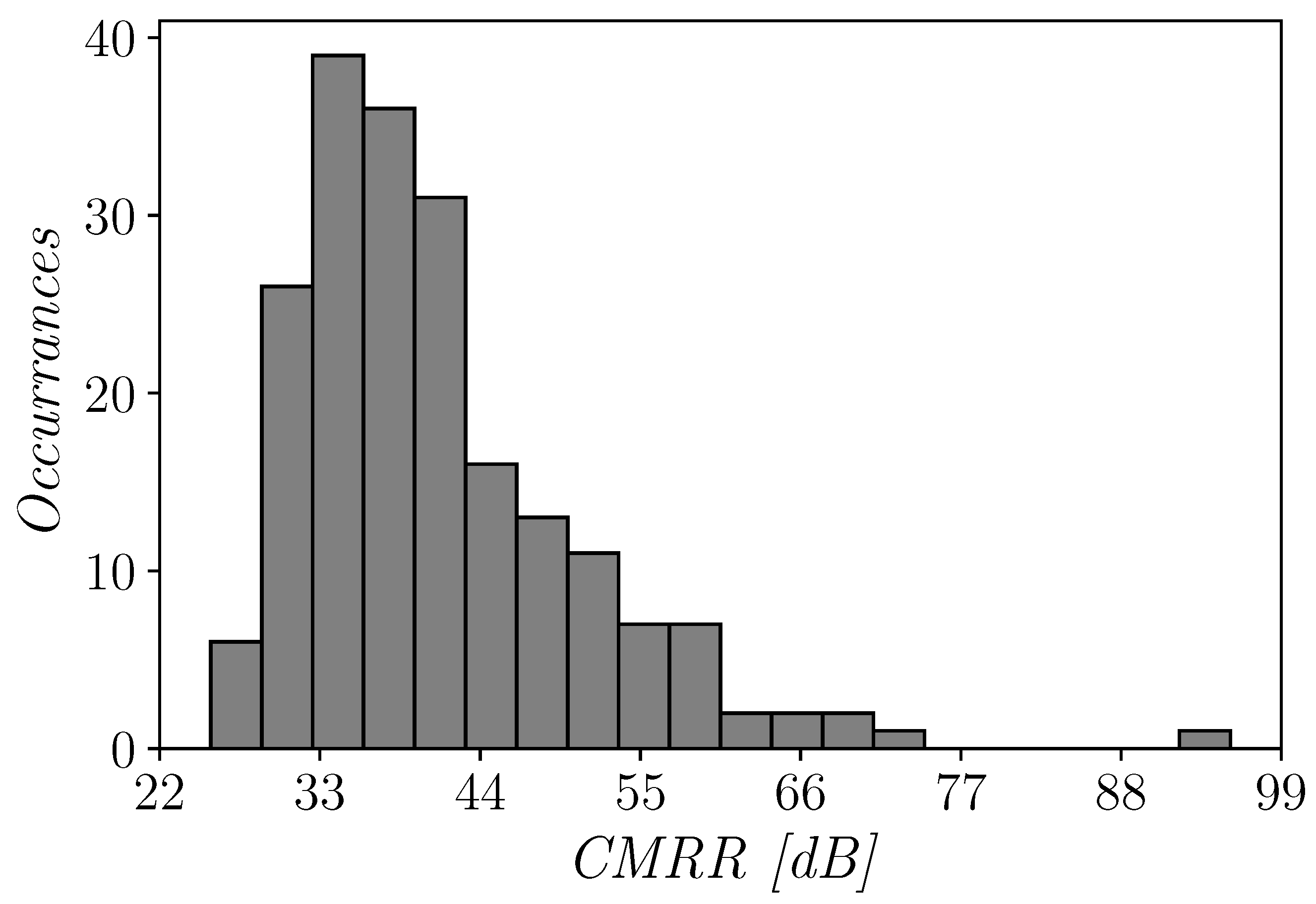
4.3. Robustness to Mismatch and PVT Variations
4.4. Discussion and Comparison with the Literature
5. Conclusions
Author Contributions
Funding
Conflicts of Interest
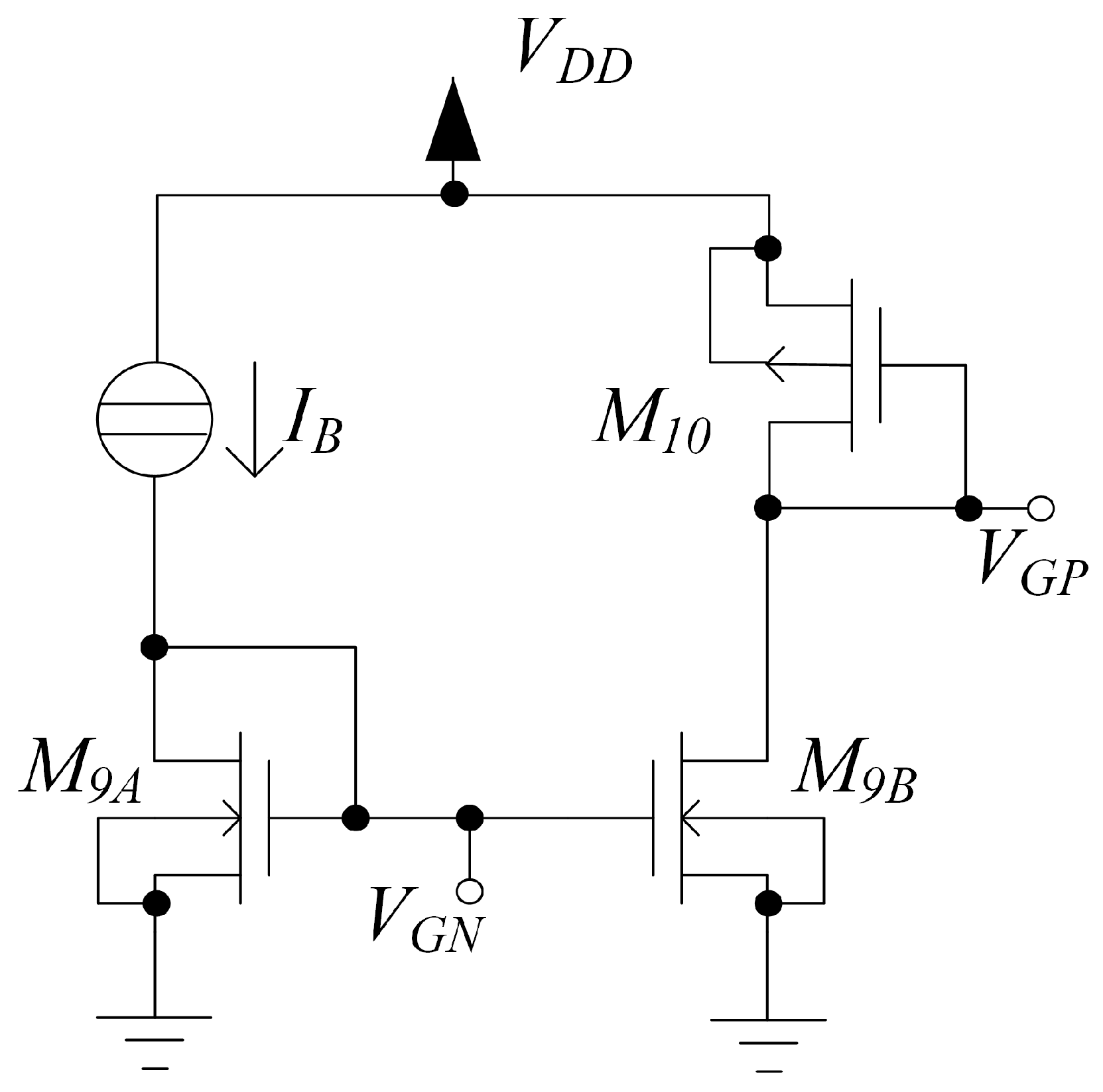
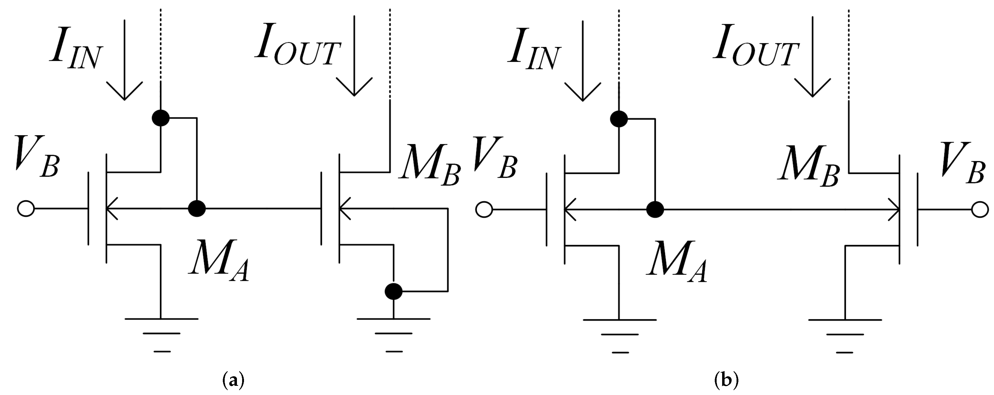
Appendix A. Body-to-Gate (B2G) Interface

Appendix B. Body-to-Body (B2B) Mirror
References
- Alioto, M. Enabling the Internet of Things—From Integrated Circuits to Integrated Systems; Springer: Berlin/Heidelberg, Germany, 2017. [Google Scholar]
- Sobin, C.C. A survey on architecture, protocols and challenges in IoT. Wirel. Pers. Commun. 2020, 112, 1383–1429. [Google Scholar] [CrossRef]
- Wu, T.; Wu, F.; Redouté, J.M.; Yuce, M.R. An autonomous wireless Body Area Network implementation towards IoT connected healthcare applications. IEEE Access 2017, 5, 11413–11422. [Google Scholar] [CrossRef]
- Lee, J.; Johnson, M.; Kipke, D. A tunable biquad switched-capacitor amplifier-filter for neural recording. IEEE Trans. Biomed. Circuits Syst. 2010, 4, 295–300. [Google Scholar] [CrossRef] [PubMed]
- Della Sala, R.; Monsurrò, P.; Scotti, G.; Trifiletti, A. Area-efficient low-power bandpass Gm-C filter for epileptic seizure detection in 130 nm CMOS. In Proceedings of the 26th IEEE International Conference on Electronics, Circuits and Systems (ICECS), Genoa, Italy, 27–29 November 2019; pp. 298–301. [Google Scholar]
- Liu, Z.; Tan, Y.; Li, H.; Jiang, H.; Liu, J.; Liao, H. A 0.5-V 3.69-nW complementary source-follower-C based low-pass filter for wearable biomedical applications. IEEE Trans. Circuits Syst. I Regul. Pap. 2020, 67, 4370–4381. [Google Scholar] [CrossRef]
- Swaroop, K.N.; Chandu, K.; Gorrepotu, R.; Deb, S. A health monitoring system for vital signs using IoT. Internet Things 2019, 5, 116–129. [Google Scholar] [CrossRef]
- Toledo, P.; Rubino, R.; Musolino, F.; Crovetti, P. Re-thinking analog integrated circuits in digital terms: A new design concept for the IoT era. IEEE Trans. Circuits Syst. II Express Briefs 2021, 68, 816–822. [Google Scholar] [CrossRef]
- Aiello, O.; Crovetti, P.; Alioto, M. Ultra-low power and minimal design effort interfaces for the Internet of Thing. In Proceedings of the ICSyS19IEEE International Circuits and Systems Symposium (ICSyS), Kuantan, Malaysia, 18–19 September 2019; pp. 1–4. [Google Scholar]
- Harpe, P.; Gao, H.; Dommele, R.; Cantatore, E.; van Roermund, A.H.M. A 0.20 mm2 3 nW signal acquisition IC for miniature sensor nodes in 65 nm CMOS. IEEE J. Solid-State Circuits 2016, 51, 240–248. [Google Scholar] [CrossRef] [Green Version]
- Chi, Q.; Yan, H.; Zhang, C.; Pang, Z.; Xu, L.D. A reconfigurable smart sensor interface for industrial WSN in IoT environment. IEEE Trans. Ind. Inform. 2014, 10, 1417–1425. [Google Scholar] [CrossRef]
- Grasso, A.D.; Pennisi, S. Ultra-low power amplifiers for IoT nodes. In Proceedings of the ICECS18 IIEEE International Conference on Electronics, Circuits and Systems (ICECS), Bordeaux, France, 9–12 December 2018; pp. 497–500. [Google Scholar]
- Richelli, A.; Colalongo, L.; Kovacs-Vajna, Z.; Calvetti, G.; Ferrari, D.; Finanzini, M.; Pinetti, S.; Prevosti, E.; Savoldelli, J.; Scarlassara, S. A survey of low voltage and low power amplifier topologies. J. Low Power Electron. Appl. 2018, 8, 22. [Google Scholar] [CrossRef] [Green Version]
- Khateb, F.; Dabbous, S.B.A.; Vlassis, S. A survey of non-conventional techniques for Low-voltage Low-power analog circuit design. Radioengineering 2013, 22, 415–427. [Google Scholar]
- Cabrera-Bernal, E.; Pennisi, S.; Grasso, A.D.; Torralba, A.; Carvajal, R.G. 0.7-V three-stage class-AB CMOS operational transconductance amplifier. IEEE Trans. Circuits Syst. I Regul. Pap. 2016, 63, 1807–1815. [Google Scholar] [CrossRef]
- Taherzadeh-Sani, M.; Hamoui, A.A. A 1-V process-insensitive current-scalable two-stage opamp with enhanced DC gain and settling behavior in 65-nm digital CMOS. IEEE J. Solid-State Circuits 2011, 46, 660–668. [Google Scholar] [CrossRef]
- Paul, A.; Ramirez-Angulo, J.; Lopez-Martin, A.J.; Carvajal, R.G.; Rocha-Perez, J.M. Pseudo-three-stage Miller op-amp with enhanced small-signal and large-signal performance. IEEE Trans. Very Large Scale Integr. (VLSI) Syst. 2019, 27, 2246–2259. [Google Scholar] [CrossRef]
- Riad, J.; Estrada-López, J.J.; Padilla-Cantoya, I.; Sánchez-Sinencio, E. Power-scaling output-compensated three-stage OTAs for wide load range applications. IEEE Trans. Circuits Syst. I Regul. Pap. 2020, 67, 2180–2192. [Google Scholar] [CrossRef]
- Wang, Y.; Zhang, Q.; Yu, S.S.; Zhao, X.; Trinh, H.; Shi, P. A robust local positive feedback based performance enhancement strategy for non-recycling folded cascode OTA. IEEE Trans. Circuits Syst. I Regul. Pap. 2020, 67, 2897–2908. [Google Scholar] [CrossRef]
- Centurelli, F.; Della Sala, R.; Monsurrò, P.; Scotti, G.; Trifiletti, A. A novel OTA architecture exploiting current gain stages to Boost bandwidth and slew-rate. Electronics 2021, 10, 1638. [Google Scholar] [CrossRef]
- Aguirre, P.C.D.; Susin, A.A. PVT compensated inverter-based OTA for low-voltage CT sigma-delta modulators. Electron. Lett. 2018, 54, 1264–1266. [Google Scholar] [CrossRef]
- Braga, R.A.; Ferreira, L.H.; Coletta, G.D.; Dutra, O.O. A 0.25-V calibration-less inverter-based OTA for low-frequency Gm-C applications. Microelectron. J. 2019, 83, 62–72. [Google Scholar] [CrossRef]
- Lv, L.; Zhou, X.; Qiao, Z.; Li, Q. Inverter-based subthreshold amplifier techniques and their application in 0.3-V ΣΔ-modulator. IEEE J. Solid-State Circuits 2019, 54, 1436–1445. [Google Scholar] [CrossRef]
- Manfredini, G.; Catania, A.; Benvenuti, L.; Cicalini, M.; Piotto, M.; Bruschi, P. Ultra-low-voltage inverter-based amplifier with novel common-mode stabilization loop. Electronics 2020, 9, 1019. [Google Scholar] [CrossRef]
- Rodovalho, L.H.; Aiello, O.; Rodrigues, C.R. Ultra-low-voltage inverter-based operational transconductance amplifiers with Voltage gain enhancement by improved composite transistors. Electronics 2020, 9, 1410. [Google Scholar] [CrossRef]
- Rodovalho, L.H.; Rodrigues, C.R.; Aiello, O. Self-biased and supply-voltage scalable inverter-based operational transconductance amplifier with improved composite transistors. Electronics 2021, 10, 935. [Google Scholar] [CrossRef]
- Baghtash, H.F. A 0.4 V, body-driven, fully differential, tail-less OTA based on current push-pull. Microelectron. J. 2020, 99, 104768. [Google Scholar] [CrossRef]
- Ghosh, S.; Bhadauria, V. An ultra-low-power near rail-to-rail pseudo-differential subthreshold gate-driven OTA with improved small and large signal performances. Analog. Integr. Circuits Signal Process. 2021, 109, 345–366. [Google Scholar] [CrossRef]
- Allen, P.E.; Blalock, B.J.; Rincon, G.A. 1 V CMOS opamp using bulk-driven MOSFETs. In Proceedings of the ISSCC’95-International Solid-State Circuits Conference, San Francisco, CA, USA, 15–17 February 1995; pp. 192–193. [Google Scholar] [CrossRef]
- Blalock, B.J.; Allen, P.E.; Rincon-Mora, G.A. Designing 1-V op amps using standard digital CMOS technology. IEEE Trans. Circuits Syst. II Analog. Digit. Signal Process. 1998, 45, 769–780. [Google Scholar] [CrossRef] [Green Version]
- Stockstad, T.; Yoshizawa, H. A 0.9-V 0.5-/spl mu/A rail-to-rail CMOS operational amplifier. IEEE J. Solid-State Circuits 2002, 37, 286–292. [Google Scholar] [CrossRef]
- Ferreira, L.; Sonkusale, S. A 60-dB gain OTA operating at 0.25-V power supply in 130-nm digital CMOS process. IEEE Trans. Circuits Syst. I Regul. Pap. 2014, 61, 1609–1617. [Google Scholar] [CrossRef]
- Colletta, G.D.; Ferreira, L.H.; Pimenta, T.C. A 0.25-V 22-nS symmetrical bulk-driven OTA for low-frequency G_m G m-C applications in 130-nm digital CMOS process. Analog. Integr. Circuits Signal Process. 2014, 81, 377–383. [Google Scholar] [CrossRef]
- Abdelfattah, O.; Roberts, G.W.; Shih, I.; Shih, Y.C. An ultra-low-voltage CMOS process-insensitive self-biased OTA with rail-to-rail input range. IEEE Trans. Circuits Syst. I Regul. Pap. 2015, 62, 2380–2390. [Google Scholar] [CrossRef]
- Akbari, M.; Hashemipour, O. A 63-dB gain OTA operating in subthreshold with 20-nW power consumption. Int. J. Circuit Theory Appl. 2017, 45, 843–850. [Google Scholar] [CrossRef]
- Veldandi, H.; Shaik, R.A. A 0.3-V pseudo-differential bulk-input OTA for low-frequency applications. Circuits Syst. Signal Process. 2018, 37, 5199–5221. [Google Scholar] [CrossRef]
- Kulej, T.; Khateb, F. A 0.3-V 98-dB Rail-to-Rail OTA in 0.18 μm CMOS. IEEE Access 2020, 8, 27459–27467. [Google Scholar] [CrossRef]
- Woo, K.C.; Yang, B.D. A 0.25-V rail-to-rail three-stage OTA with an enhanced DC gain. IEEE Trans. Circuits Syst. II Express Briefs 2020, 67, 1179–1183. [Google Scholar] [CrossRef]
- Centurelli, F.; Della Sala, R.; Scotti, G.; Trifiletti, A. A 0.3 V, rail-to-rail, ultralow-power, non-tailed, body-driven, sub-tThreshold amplifier. Appl. Sci. 2021, 11, 2528. [Google Scholar] [CrossRef]
- Centurelli, F.; Della Sala, R.; Monsurrò, P.; Scotti, G.; Trifiletti, A. A 0.3 V rail-to-rail ultra-low-power OTA with improved bandwidth and slew rate. J. Low Power Electron. Appl. 2021, 11, 19. [Google Scholar] [CrossRef]
- Fortes, A.; Quirino, F.A.; da Silva, L.A.; Girardi, A. Low power bulk-driven OTA design optimization using cuckoo search algorithm. Analog. Integr. Circuits Signal Process. 2021, 106, 99–109. [Google Scholar] [CrossRef]
- Centurelli, F.; Della Sala, R.; Monsurró, P.; Tommasino, P.; Trifiletti, A. An ultra-low-voltage class-AB OTA exploiting local CMFB and body-to-gate interface. AEU Int. J. Electron. Commun. 2022, 145, 154081. [Google Scholar] [CrossRef]
- Crovetti, P.S. A digital-based analog differential circuit. IEEE Trans. Circuits Syst. I Regul. Pap. 2013, 60, 3107–3116. [Google Scholar] [CrossRef]
- Toledo, P.; Crovetti, P.; Aiello, O.; Alioto, M. Fully digital rail-to-rail OTA with sub-1000-μm² area, 250-mV minimum supply, and nW power at 150-pF load in 180 nm. IEEE Solid-State Circuits Lett. 2020, 3, 474–477. [Google Scholar] [CrossRef]
- Toledo, P.; Crovetti, P.; Aiello, O.; Alioto, M. Design of digital OTAs with operation down to 0.3 V and nW power for direct harvesting. IEEE Trans. Circuits Syst. I Regul. Pap. 2021, 68, 3693–3706. [Google Scholar] [CrossRef]
- Toledo, P.; Crovetti, P.; Klimach, H.; Bampi, S.; Aiello, O.; Alioto, M. 300mV-supply, sub-nW-power digital-based operational transconductance amplifier. IEEE Trans. Circuits Syst. II Express Briefs 2021, 68, 3073–3077. [Google Scholar] [CrossRef]
- Toledo, P.; Crovetti, P.; Klimach, H.; Bampi, S. Dynamic and static calibration of ultra-low-voltage, digital-based operational transconductance amplifiers. Electronics 2020, 9, 983. [Google Scholar] [CrossRef]
- Fiorelli, R.; Arnaud, A.; Galup-Montoro, C. Series-parallel association of transistors for the reduction of random offset in non-unity gain current mirrors. In Proceedings of the ISCAS04 IEEE International Symposium on Circuits and Systems, Vancouver, BC, Canada, 23–26 May 2004; Volume 1, pp. 881–884. [Google Scholar]
- Narasimman, N.; Kim, T.T. A 0.3 V, 49 fJ/conv.-step VCO-based delta sigma modulator with self-compensated current reference for variation tolerance. In Proceedings of the ESSCIRC Conference 2016: 42nd European Solid-State Circuits Conference, Lausanne, Switzerland, 12–15 September 2016; pp. 237–240. [Google Scholar] [CrossRef]
- Kulej, T.; Khateb, F. A compact 0.3-V class AB bulk-driven OTA. IEEE Trans. Very Large Scale Integr. (VLSI) Syst. 2020, 28, 224–232. [Google Scholar] [CrossRef]
- Kulej, T.; Khateb, F. Design and implementation of sub 0.5-V OTAs in 0.18-μm CMOS. Int. J. Circuit Theory Appl. 2018, 46, 1129–1143. [Google Scholar] [CrossRef]


| Transistor | Stage | Width [m] | Length [m] | I [nA] |
|---|---|---|---|---|
| M, M | 1 | 4.465 | 1.000 | 4 |
| M, M, M, M | 1 | 0.375 | 3.000 | 4 |
| M, M, M | 2 | 4.465 | 1.000 | 4 |
| M, M | 2 | 0.375 | 3.000 | 4 |
| M, M, M, M | 3 | 13.390 | 1.000 | 19.67 |
| M, M, M, M | 3 | 1.125 | 3.000 | 19.67 |
| Mean | StdDev | Min | Max | |
|---|---|---|---|---|
| P (nW) | 20.85 | 1.44 | 16.6 | 24.34 |
| Idiss (nA) | 69.50 | 4.80 | 55.33 | 81.13 |
| Offset (mV) | 3.84 | 15.46 | −30 | 50 |
| SR (V/ms) | 18.54 | 0.30 | 17.84 | 19.42 |
| SR (V/ms) | 11.63 | 0.34 | 10.82 | 12.52 |
| Gain (1 Hz) (dB) | 51.48 | 1.22 | 49.59 | 56.49 |
| CMRR (dB) | 42.11 | 10.44 | 27.84 | 98.85 |
| PSRR (dB) | 56.13 | 2.12 | 48.05 | 56.39 |
| Mphi (deg) | 53.08 | 6.27 | 38.25 | 74.98 |
| GBW (kHz) | 32.72 | 8.42 | 11.54 | 49.33 |
| THD (%) | 0.74 | 0.57 | 0.51 | 2.61 |
| Temp (°C) | 0.00 | 16.67 | 27.00 | 43.33 | 50.00 | 70.00 |
|---|---|---|---|---|---|---|
| P (nW) | 21.48 | 21.93 | 21.89 | 20.40 | 20.54 | 21.35 |
| I (nW) | 71.59 | 73.10 | 72.98 | 68.00 | 68.46 | 71.18 |
| SR (V/ms) | 11.44 | 15.66 | 18.61 | 23.55 | 25.60 | 31.76 |
| SR (V/ms) | 10.11 | 10.99 | 11.51 | 12.47 | 12.84 | 13.65 |
| Gain (1Hz) (dB) | 58.65 | 57.61 | 52 | 50.07 | 48.87 | 46.72 |
| CMRR (dB) | 64.45 | 57.56 | 44.96 | 34.31 | 32.03 | 26.66 |
| Mphi (deg) | 48.63 | 46.26 | 52.40 | 54.54 | 52.86 | 48.88 |
| GBW (kHz) | 32.85 | 39.45 | 35.16 | 30.80 | 32.16 | 37.95 |
| Noise (/) | 0.60 | 0.85 | 1.60 | 3.42 | 3.91 | 4.85 |
| THD (%) | 0.45 | 0.51 | 0.67 | 0.72 | 0.84 | 1.23 |
| V (mV) | 270.0 | 285.0 | 300.0 | 315.0 | 330.0 |
|---|---|---|---|---|---|
| P (nW) | 21.710 | 21.980 | 21.890 | 20.500 | 20.240 |
| Idiss (nA) | 72.370 | 73.270 | 72.980 | 68.350 | 67.460 |
| SR (V/ms) | 8.532 | 12.750 | 18.610 | 26.500 | 36.790 |
| SR (V/ms) | 7.147 | 9.161 | 11.510 | 14.230 | 17.210 |
| Gain (1 Hz) (dB) | 54.34 | 53.22 | 52.93 | 52.84 | 53.07 |
| CMRR (dB) | 60.340 | 53.720 | 44.960 | 38.740 | 35.450 |
| Mphi (deg) | 47.530 | 50.230 | 52.920 | 53.550 | 49.570 |
| GBW (kHz) | 34.830 | 35.230 | 35.160 | 33.470 | 36.980 |
| Noise (/) | 0.869 | 1.011 | 1.595 | 2.485 | 3.161 |
| THD (%) | 0.50 | 0.37 | 0.29 | 0.23 | 0.19 |
| Corner | TYP | FF | SS | SF | FS |
|---|---|---|---|---|---|
| P (nW) | 21.89 | 20.32 | 21.68 | 21.98 | 26.60 |
| Idiss (nA) | 72.97 | 67.73 | 72.27 | 73.27 | 88.67 |
| SR (V/ms) | 18.61 | 27.32 | 12.18 | 28.77 | 11.63 |
| SR (V/ms) | 11.51 | 15.47 | 8.62 | 9.00 | 14.43 |
| Gain (1 Hz)(dB) | 52.92 | 50.41 | 57.90 | 55.72 | 49.93 |
| CMRR (dB) | 44.96 | 33.72 | 63.31 | 53.26 | 35.5 |
| PSRR (dB) | 56.40 | 48.26 | 73.31 | 64.93 | 47.52 |
| Mphi (deg) | 52.40 | 51.37 | 48.59 | 42 | 58.59 |
| GBW (kHz) | 35.16 | 34.43 | 37.19 | 49.626 | 27.55 |
| Noise (/) | 1.60 | 3.03 | 3.03 | 3.21 | 5.16 |
| THD (%) | 0.67 | 0.25 | 0.43 | 0.95 | 0.46 |
| This Work * | [42] * | [45] | [40] * | [39] * | [25] * | [37] | [50] | [23] | [36] * | [51] | |
|---|---|---|---|---|---|---|---|---|---|---|---|
| Year | 2021 | 2021 | 2021 | 2021 | 2021 | 2020 | 2020 | 2019 | 2019 | 2018 | 2018 |
| Technology (m) | 0.13 | 0.13 | 0.18 | 0.13 | 0.13 | 0.18 | 0.18 | 0.18 | 0.13 | 0.065 | 0.18 |
| (V) | 0.3 | 0.3 | 0.3 | 0.3 | 0.3 | 0.3 | 0.3 | 0.3 | 0.3 | 0.3 | 0.3 |
| 0.86 | 0.86 | 0.6 | 0.86 | 0.86 | 0.6 | 0.6 | 0.6 | 0.86 | - | 0.6 | |
| (dB) | 52.92 | 38.07 | 30 | 40.80 | 64.6 | 39 | 98.1 | 64.7 | 49.8 | 60 | 65.8 |
| (pF) | 50 | 50 | 150 | 40 | 50 | 10 | 30 | 30 | 2 | 5 | 20 |
| GBW (kHz) | 35.16 | 24.14 | 0.25 | 18.65 | 3.58 | 0.9 | 3.1 | 2.96 | 9100 | 70 | 2.78 |
| (deg) | 52.40 | 60.15 | 90 | 51.93 | 53.76 | 90 | 54 | 52 | 76 | 53 | 61 |
| 18.61 | 20.02 | - | 10.83 | 1.7 | - | 14 | 1.9 | - | 25 | 6.44 | |
| 11.51 | 8.44 | - | 32.37 | 0.15 | - | 4.2 | 6.4 | - | 25 | 7.8 | |
| 15.06 | 14.23 | 0.085 | 21.60 | 0.93 | - | 9.1 | 4.15 | 3.8 | 25 | 7.12 | |
| THD (%) | 0.673 | 1.635 | 2 | 1.4 | 0.84 | 1 | 0.49 | 1 | - | - | 1 |
| % of input swing | 90 | 80 | 90 | 80 | 100 | 23 | 83.33 | 85 | - | - | 93.33 |
| CMRR (dB) | 42.11 | 54.88 | 41 | 67.49 | 61 | 30 | 60 | 110 | - | 126 | 72 |
| PSRR (dB) | 56.13 | 51.05 | 30 | 45 | 26/28 | 33 | 61 | 56 | - | 90/91 | 62 |
| spot-noise | 1.60 | 3.16 | - | 2.12 | 2.69 | 0.81 | 1.8 | 1.6 | 0.035 | 2.82 | 1.85 |
| @freq (Hz) | 1000 | 1000 | - | 1000 | 100 | 1000 | - | - | 100,000 | 1000 | 36 |
| Power (nW) | 21.89 | 59.88 | 2.4 | 73 | 11.4 | 0.6 | 13 | 12.6 | 1800 | 51 | 15.4 |
| Mode | BD | BD | DIGITAL | BD | BD | GD | BD | BD | GD | BD | BD |
| 80.29 k | 20.16 k | 15.89 k | 10.20 k | 15.72 k | 15.00 k | 7.15 k | 7.05 k | 10.11 k | 6.86 k | 3.61 k | |
| 34.40 k | 11.88 k | 5.40 k | 11.82 k | 4.08 k | - | 21.00 k | 9.88 k | 4.67 k | 2.45 k | 9.25 k | |
| 26.30 k | 7.04 k | - | 5.93 k | 4.52 k | - | 6.30 k | 4.52 k | - | 2.45 k | 8.36 k | |
| Area | 0.0052 | 0.0027 | 0.000982 | 0.0036 | 0.0036 | 0.00047 | 0.0098 | 0.0085 | - | 0.003 | 0.0082 |
Publisher’s Note: MDPI stays neutral with regard to jurisdictional claims in published maps and institutional affiliations. |
© 2022 by the authors. Licensee MDPI, Basel, Switzerland. This article is an open access article distributed under the terms and conditions of the Creative Commons Attribution (CC BY) license (https://creativecommons.org/licenses/by/4.0/).
Share and Cite
Centurelli, F.; Della Sala, R.; Monsurrò, P.; Scotti, G.; Trifiletti, A. A Tree-Based Architecture for High-Performance Ultra-Low-Voltage Amplifiers. J. Low Power Electron. Appl. 2022, 12, 12. https://doi.org/10.3390/jlpea12010012
Centurelli F, Della Sala R, Monsurrò P, Scotti G, Trifiletti A. A Tree-Based Architecture for High-Performance Ultra-Low-Voltage Amplifiers. Journal of Low Power Electronics and Applications. 2022; 12(1):12. https://doi.org/10.3390/jlpea12010012
Chicago/Turabian StyleCenturelli, Francesco, Riccardo Della Sala, Pietro Monsurrò, Giuseppe Scotti, and Alessandro Trifiletti. 2022. "A Tree-Based Architecture for High-Performance Ultra-Low-Voltage Amplifiers" Journal of Low Power Electronics and Applications 12, no. 1: 12. https://doi.org/10.3390/jlpea12010012