1. Introduction
Over the past decade, low temperature polycrystalline silicon thin film transistors (poly-Si TFTs) fabricated on glass substrates have attracted a great deal of attention in active-matrix organic light emitting (AMOLED) display and active-matrix liquid crystal (AMLCD) display applications, as well as peripheral driving circuits, because of their high electron mobility and large driving current [
1,
2]. The main problem for poly-Si TFT is that it experiences a very high drain electric field near the channel/drain area, resulting in a very serious leakage current and a profound kink effect in its I-V characteristics, which limits the device’s performance in circuit applications [
3,
4,
5]. The main approach to lower the leakage current and suppress the kink effect is to reduce the device drain side electric field. Several designs have been proposed and studied to reduce the drain electric field and improve device performance, including offset gate [
6,
7], lightly-doped drain (LDD) [
8,
9], and field-induced drain (FID) [
10,
11] TFTs. However, offset gate TFT sacrifices the On-state current, due to an increased parasitic resistance, and FID design often needs an extra mask and one more field bias, which complicates the device biasing scheme. In the same vein, the LDD structure has higher On-state current than the offset one and the LDD design often needs additional implantation process and suffers ion implantation damage and difficulty in controlling the doping in grain boundary [
7,
8,
12]. A raised source/drain (RSD) structure is an alternative approach to lower device leakage current and drain side electric field effectively, without degrading On-state current seriously [
4,
12]. However, conventional RSD TFTs, which have thicker source/drain regions with a thin channel, are usually not a self-aligned structure and need an extra mask [
13]. Although a self-aligned RSD device can be produced by a damascene process method, it involves more complex fabrication steps, including more chemical mechanical polishing (CMP) processes [
12].
Our previous studies have proposed a drain-extended field plate structure (DFPTFT) to provide a different option to suppress the kink effect [
14]. This drain field plate design constructs a low impact ionization rate (IIR) device featuring a high current density and high electric field apart structure to dampen the kink effect. However, the device shown in [
14] has a bottom gate frame with an additional mask, making it difficult to be compatible with the present top gate structure, which is adopted in most popular poly-Si TFTs fabrications applied in industrial production. Furthermore, as a result of the almost unreduced electric field in the previous structure [
14], the leakage current is hardly reduced.
This study puts forth new current and electric field split TFT (CES-TFT) with partial thicker channel RSD [
15] and bottom field plate (BFP) designs which do not require an extra mask and CMP process. The BFP connected to the drain can allure the electron and change the electron current path away from the high electric field area in the gate/drain region, thereby alleviating the impact ionization phenomenon. In addition, the partial thicker channel RSD structure in use is also conducive to reducing the drain electric field that contributes to the lowering of leakage current and suppression of the kink effect [
15].
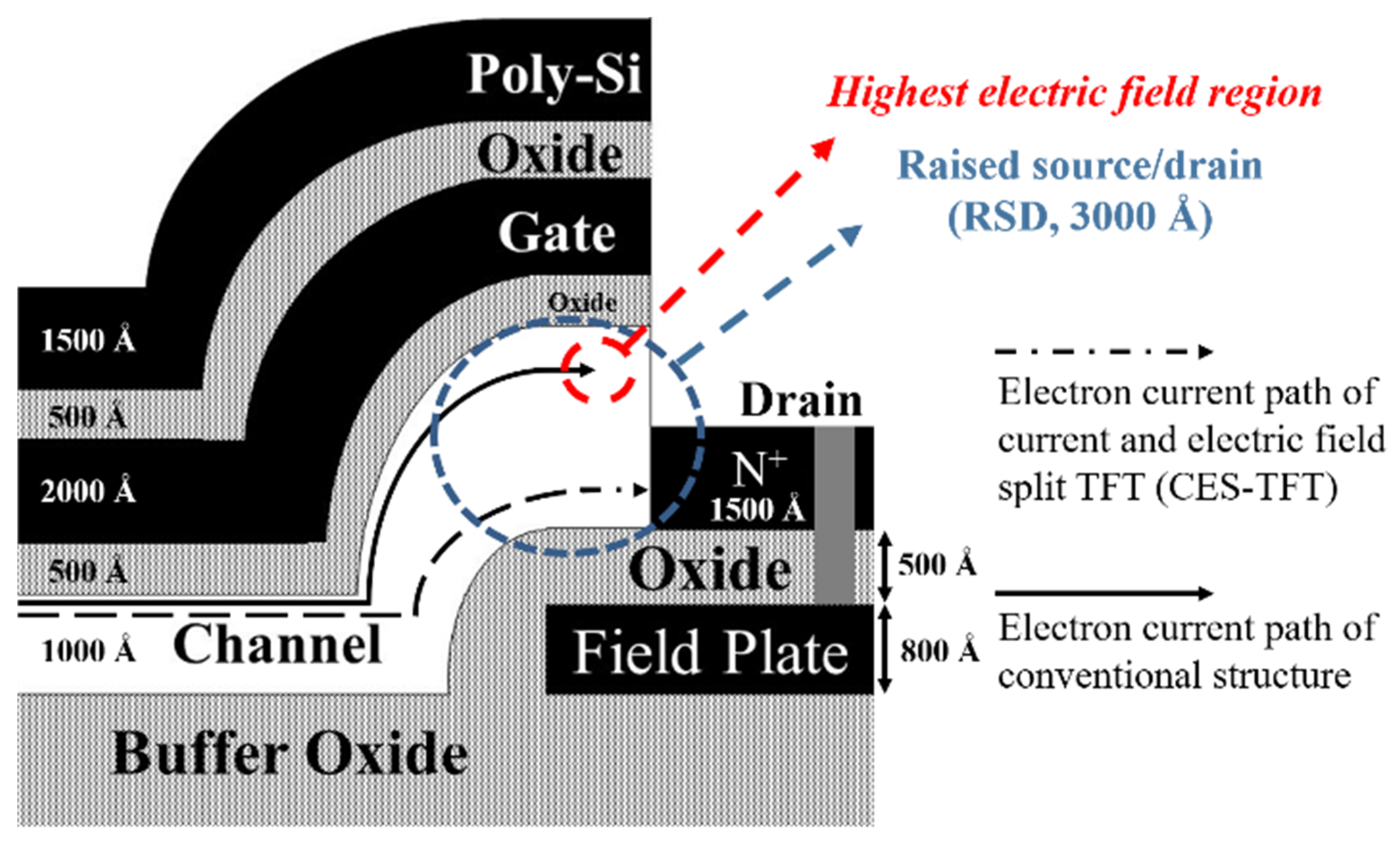
Figure 1 shows the design information and half cross section of the proposed structure. When the drain voltage (
Vds) is lower than the gate voltage (
Vgs), the current path will flow along the gate side channel. The current path will be changed once
Vds is higher than
Vgs owing to a smaller channel resistance near the top area of the field plate.
2. Device Fabrication
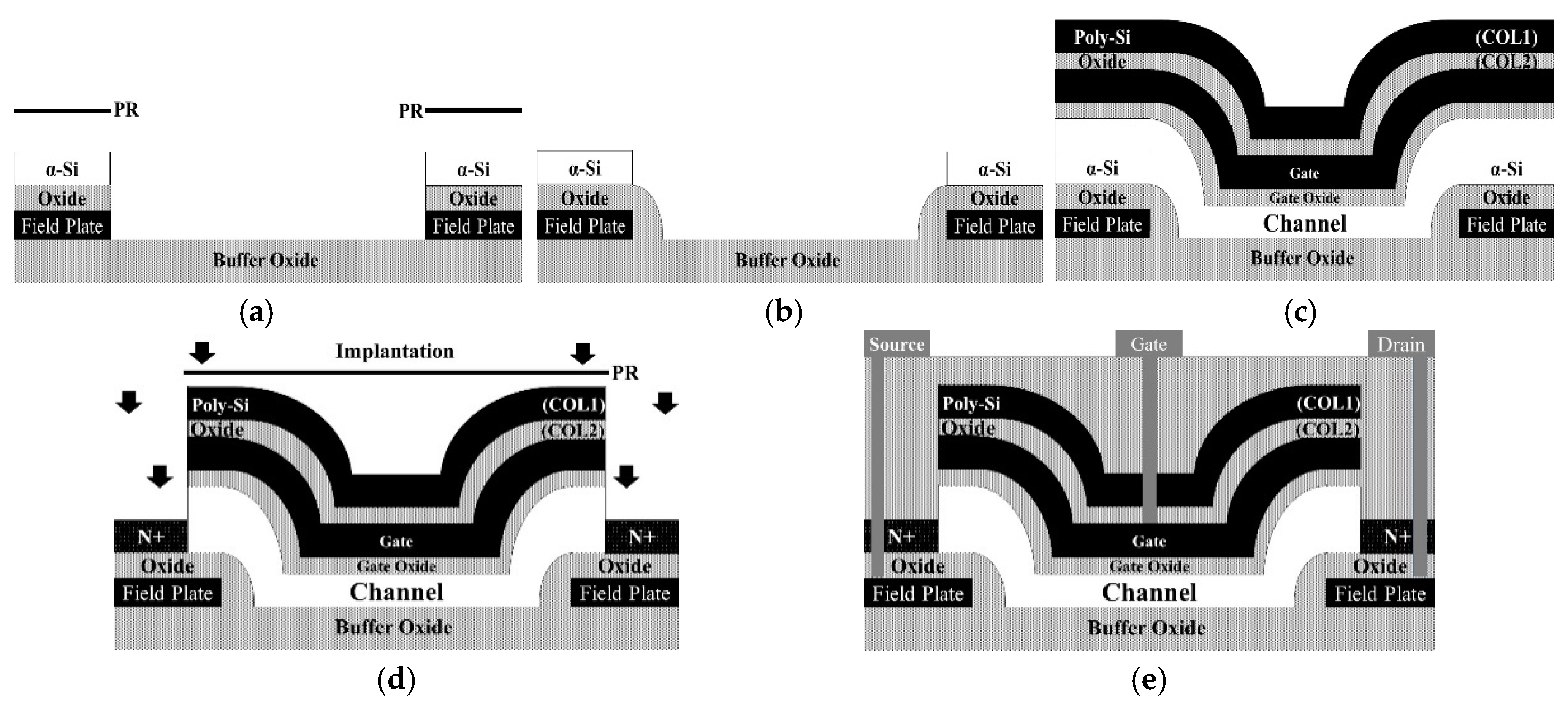
To fabricate the device, a heavy doped poly-Si layer with 800 Å was first deposited to be the BFP on an oxidized silicon wafer. Then, an oxide (500 Å) and a 2000 Å undoped amorphous silicon (α-Si) were grown, in turn, forming a raised source/drain structure.
Figure 2 illustrates the key fabrication processes of this CES device. After the FP region was defined, an oxide spacer was made before depositing a 1000 Å undoped α-Si channel layer. This α-Si layer and RSD structures were then transferred into the poly-Si together via solid-phase crystallization with 24 h 600 °C treatment. Then, an oxide (500 Å), an in situ doped poly-Si (2000 Å), an oxide (500 Å), and a poly-Si layer (1500 Å) were deposited, functioning as gate oxide, gate electrode, contact open layer (COL) 2, and (COL) 1, respectively. The thickness of (COL) 2 is designed to be the same as for the oxide above the field plate. The contact open layers in use here can make the gate electrode and drain one, respectively, metal-connect to their corresponding layer in the subsequent process. First, the gate area was defined and all layers were etched until the RSD layer was removed to 1500 Å. Then, source/drain areas were formed via phosphorous implantation. A 300-nm-thick oxide was then fabricated to serve as a passivation layer, and contact holes were opened and etched from the top layer to the gate and FP layers simultaneously. Finally, an Al-Si-Cu layer was grown and defined as metal pads. There were four CES-TFT masks, fewer than in the DFPTFT [
14] proposed previously. A traditional top gate device was implemented at the same time for comparison purposes.
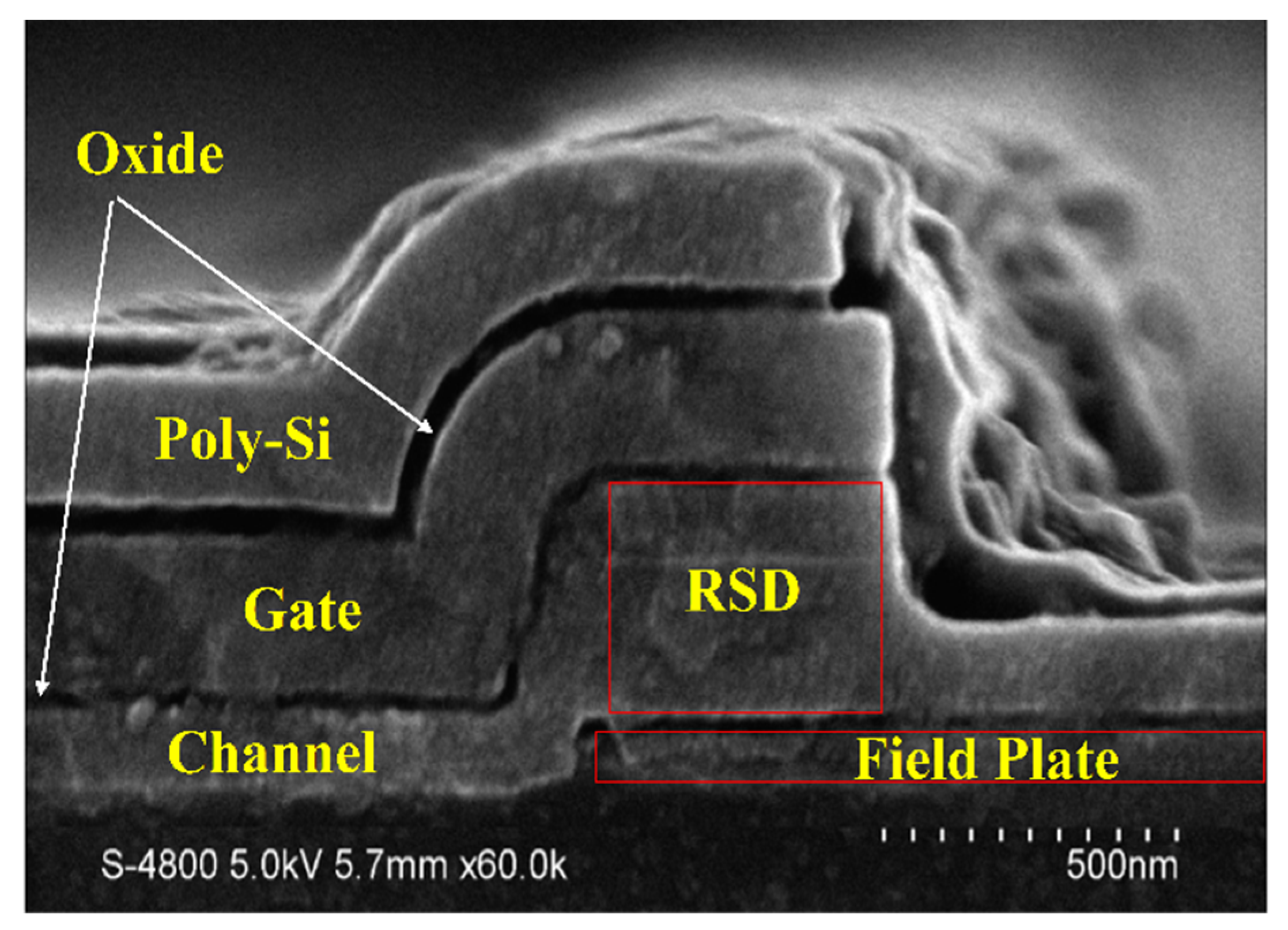
Figure 3 shows the scanning electron microscope picture of the proposed CES-TFT.
3. Structure Simulation, Device Measurement, and Discussion
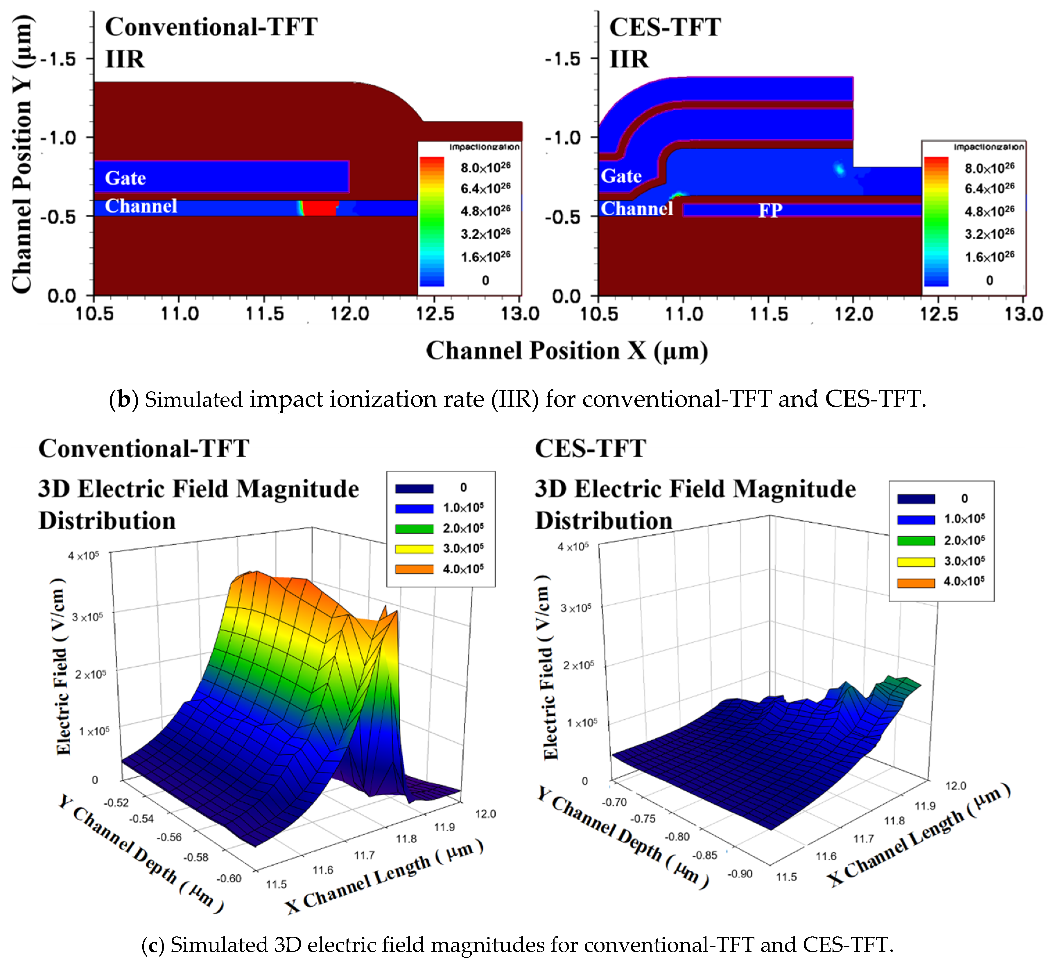
Before evaluating the device’s performance, ISE-TCAD was employed to gauge the difference between the conventional device and CES-TFT in the current path, drain electric field, and IIR [
13,
14,
15,
16]. The device IIR can be derived by a Chynoweth model and expressed [
14] as
where
Jn is the electron current density of an n-type device and the parameters
An and
Bn are the electron ionization coefficients; these values can be found in our previous publication [
14] and are used widely to model impact ionization rate [
16,
17,
18]. If device current can be designed to be far away from the highest electrical field region at a higher drain bias, a low IIR device, and a highly reliable TFT is achievable.
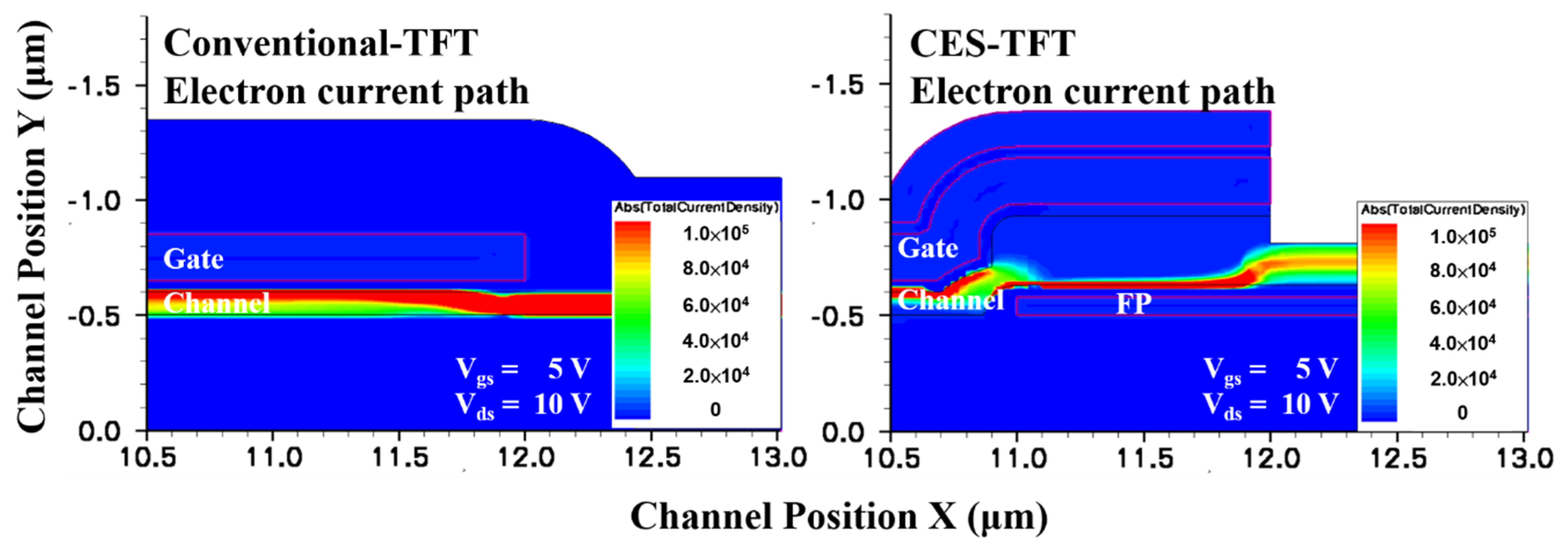
Figure 4 demonstrates the electron current path of both structures at
Vds = 10 V and
Vgs = 5 V. In
Figure 4, it can be observed that in BFP design, the electron current path is altered.
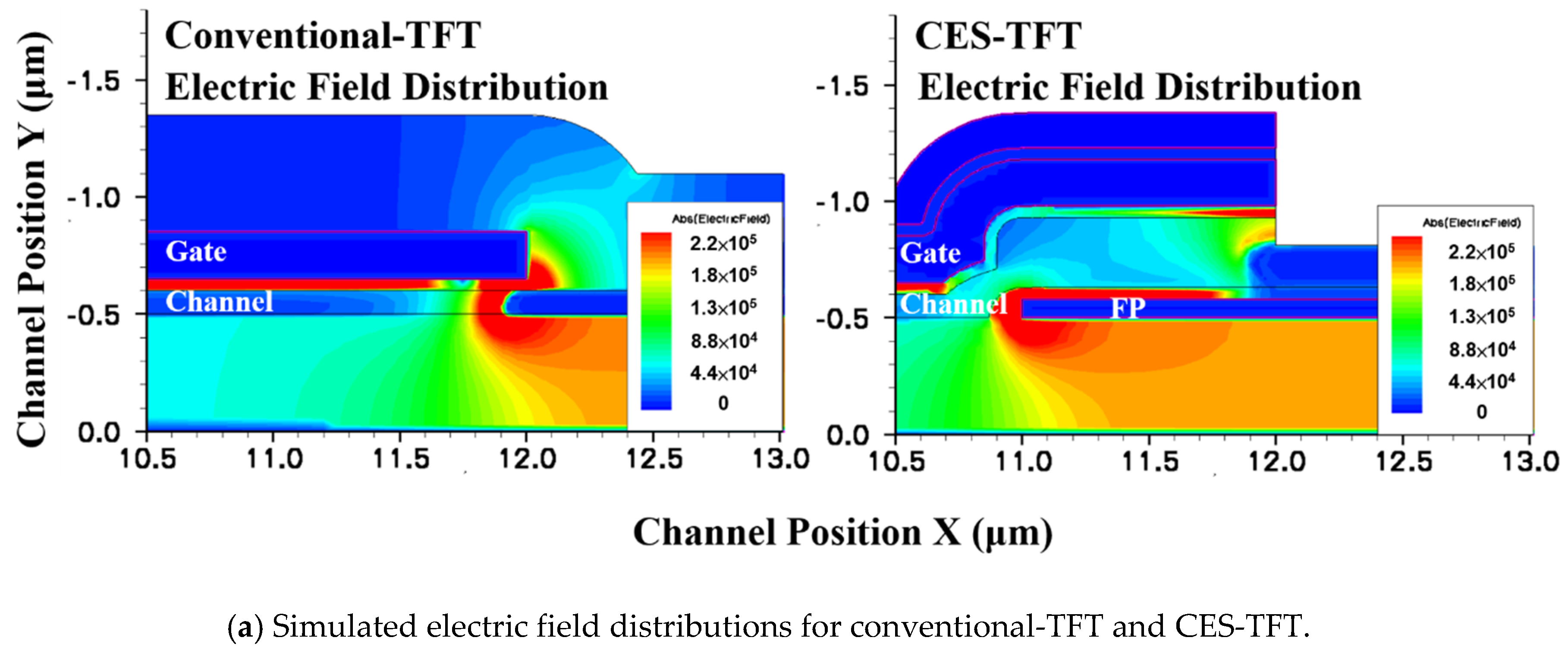
Figure 5a,b depict the simulated drain side electric field and IIR distributions of both structures as
Vds = 10 V and
Vgs = 5 V. A more clear comparison can be shown by redrawing the magnitudes of the simulated electric field near the gate/drain areas in a 3D plot.
Figure 5c shows the simulated 3D electric field for both structures. The maximum electric field (IIR) is 2.17 × 10
5 V/cm (4.54 × 10
25 cm
−3/s) for CES-TFT and 3.45 × 10
5 V/cm (2.06 × 10
28 cm
−3/s) for the conventional structure. It is clear that in the CES structure with a partial thicker channel RSD design, both the electric field and IIR can be reduced because the structure can lower the drain side electric field and the BFP design can change the current path, thereby improving the IIR significantly. From
Figure 4 and
Figure 5 it is obvious that the current path of CES-TFT can detour the highest drain electric field area and therefore reduce the IIR (over two orders of improvement). A lower IIR will be conducive to alleviate the kink effect.
Unlike the conventional CES structure mentioned in [
14], where the electric field is almost the same as the conventional device, the proposed CES-TFT with an RSD design can effectively lower the device electric field.
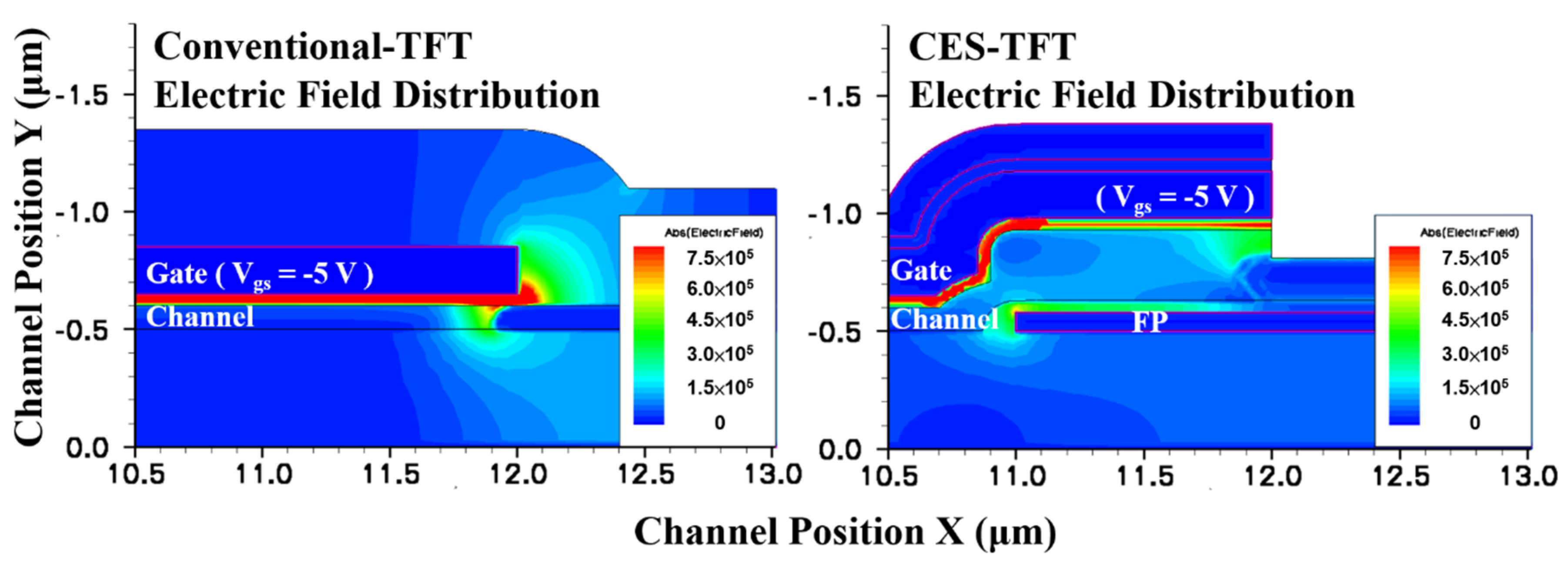
Figure 6 shows the simulated drain side electric field distributions for both structures at
Vds = 5 V and
Vgs = −5 V. The leakage characteristics for both structures can be predicted by a negative gate bias simulation. The lower negative gate bias electric field helps this structure lower the leakage current [
13,
15].
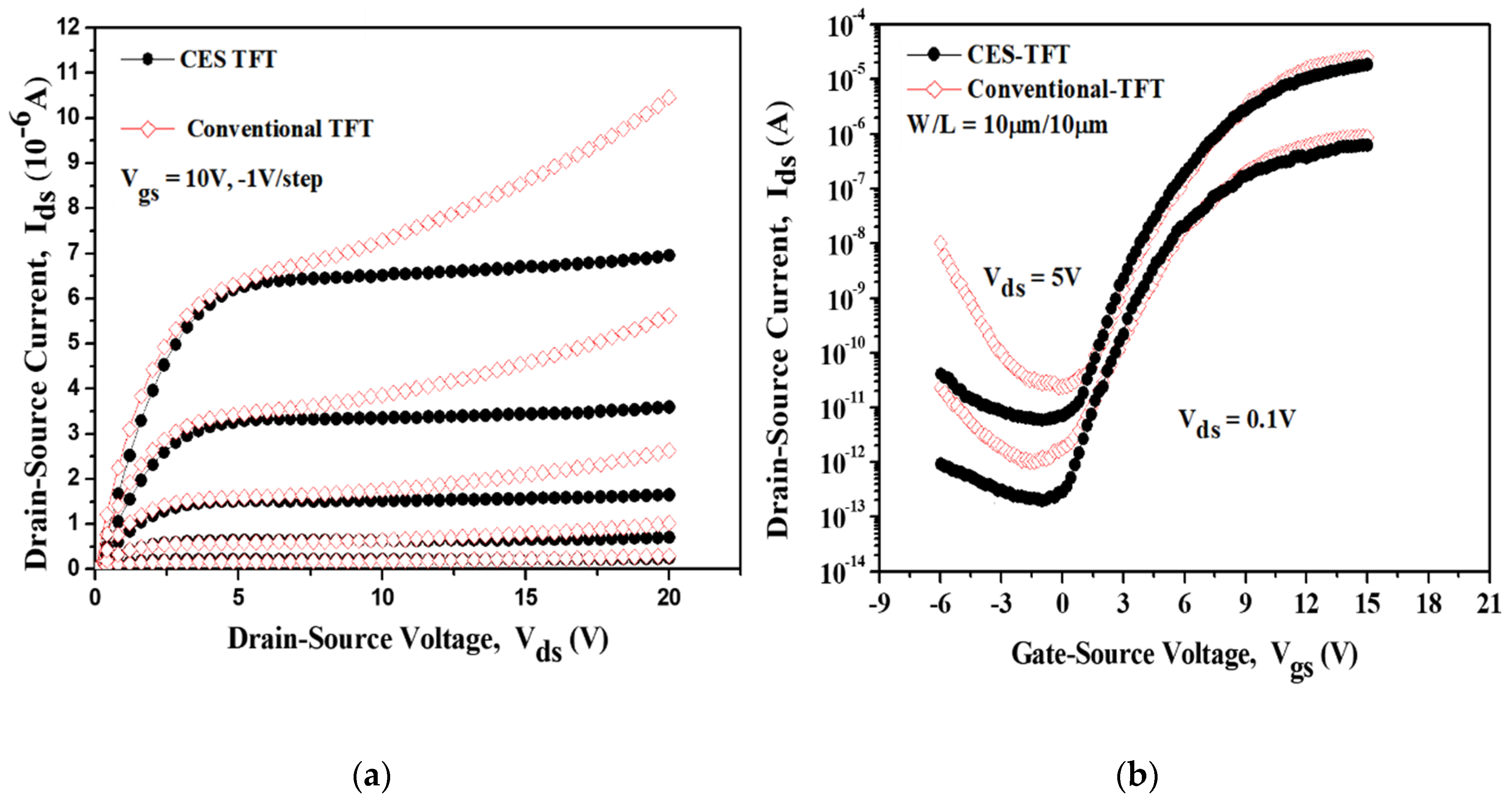
Figure 7a,b depict the measured transfer curves and device output characteristics for both structures. The leakage currents measured at
Vgs = −6 V and
Vds = 5 V for CES-TFT and conventional TFT are found to be 4.13 × 10
−11 A and 1.01 × 10
−8 A, respectively. The threshold voltages (extracted at
Vds = 0.1 V) for both devices are 5.4 V (CES-TFT) and 5.2 V (conventional TFT), those values being defined as the
Vgs at
Ids = 10 nA × (channel width (W)/channel length (L)) [
13]. It can be observed that the kink effect of the CES device is significantly mitigated because its electron current route circumvents the highest drain electric field region [
14]. The ON/OFF current ratio (defined by maximum current over minimum current) of the CES structure is 2.61 × 10
6, compared with the corresponding value of 1.03 × 10
6 for the conventional device. The improved ON/OFF current ratio stems from the reduced device electric field, which facilitates a lower leakage current.
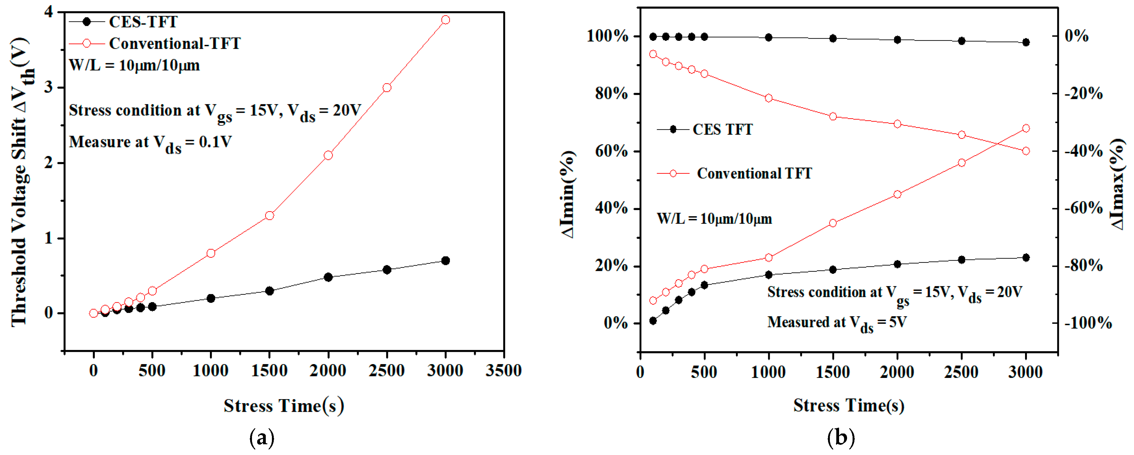
The hot-carrier stress was also carried out at
Vgs = 15 V and
Vds = 20 V with a 3000 s test to gauge the electrical reliability for both fabricated devices.
Figure 8a shows the threshold voltage (
Vth) shift of both structures after bias testing. It can be observed that the
Vth shift of the CES structure remains almost unchanged after stress. However, there is a significant change in the
Vth shift of the conventional device.
Figure 8b shows the drop in the maximum ON-current (
△Imax ) and increase in minimum drain current (
△Imax) after hot-carrier stress. Both
△Imax and
△Imin for the conventional device exhibit much higher variations than those of the CES structure after reliability stress. The
△Imax and
△Imin are 2.1% and 34.12%, respectively, for the proposed CES structure compared with the corresponding values of 39.9% and 68% for the conventional device. The experimental results show that the CES-TFT has better hot-carrier stress endurance than the conventional device thanks to the partial thicker channel RSD and CES design.

 ,
, 


