Article

Study on Local Residual Stress in a Nanocrystalline Cr2O3 Coating by Micro-Raman Spectroscopy

1
Tianjin Key Laboratory of High Speed Cutting and Precision Machining, School of Mechanical Engineering, Tianjin University of Technology and Education, Tianjin 300222, China
2
Department of Electrical and Computer Engineering, University of Delaware, Newark, DE 19716, USA
*
Authors to whom correspondence should be addressed.
Coatings 2019, 9(8), 500; https://doi.org/10.3390/coatings9080500
Submission received: 6 July 2019 / Revised: 2 August 2019 / Accepted: 5 August 2019 / Published: 7 August 2019
(This article belongs to the Special Issue Stress in Thin Films and Coatings)

Abstract

:
Residual stress in coatings often affects the service performance of coatings, and the residual stresses in some local areas even lead to premature failure of coatings. In this work, we characterized the residual stress of local micro-areas of a nanocrystalline Cr2O3 coating deposited on a Si wafer through micro-Raman spectroscopy, including the depositional edge zone where the electrode was placed, the micro-area containing Cr2O3 macroparticles, and other micro-areas vulnerable to cracks. To accurately measure the thickness of the coating, we combined optical interferometry and direct measurement by a profilometer. The results indicate the existence of in-plane tensile residual stress on the Cr2O3 coating. In thick coatings, the residual stress is independent of the coating thickness and is stable between 0.55 GPa and 0.75 GPa. As the coating thickness is less than 0.8 μm, the residual stress is directly related to the coating thickness. This in-plane tensile stress is considered as the origin of the observed microcrack, which can partially release the stress.

1. Introduction

Chromium trioxide (Cr2O3), also known as chromium oxide, is used as a functional coating in many fields for its excellent properties such as high hardness, wear resistance, corrosion resistance and low coefficient of friction [1,2,3,4]. Cr2O3 coatings are usually prepared by gas phase deposition. Along with the formation of thin films, residual stress is often introduced into the Cr2O3 coating [5], exerting a strong influence on the interface toughness, adhesion, and carrying capacity of the coating [6], thus affecting functionalities. The correlation between the film thickness and its residual strain can contribute to the understanding of the origin of the residual stress, and thus provide clues to improve the preparation method to minimize these undesired strains, as well as offer benefits to the design, manufacturing, and service performance prediction of the Cr2O3 coating.
The residual stress in the coating generally includes growth stress (caused by volume expansion or epitaxial growth) and thermal residual stress (caused by differences in thermal expansion coefficients of the substrate and the coating) [7]. In most cases, growth stress in the Cr2O3 obtained during the oxidation process is compressed; however, there have been some instances where growth stress was negligible [8]. According to an X-ray diffraction (XRD) study and a calculation of the thermal expansion coefficient mismatch between Cr2O3 and its alloy substrate, compressive thermal residual stress was observed upon cooling [8,9]. XRD, one of the most commonly used methods for measuring residual stress within a coating, obtains the residual stress based on changes in interplanar spacing detected by Bragg’s law. Since the spatial resolutions along the in-plane and thickness directions of the XRD method are greater than 100 μm and 20 μm [10], respectively, the XRD method can detect the average stress in the coating but is unable to obtain the stress distribution characteristics in tiny local areas. Also, thin coatings and uneven micro-strains in the material can lead to large measurement errors [11]. The XRD method using a synchrotron radiation source with a smaller beam diameter [12] can be used as a stress distribution measurement tool with higher spatial resolution, but obviously cannot be used at a laboratory scale. The curvature method is also commonly used to measure the residual stress on a coating [13,14,15]. It calculates the residual stress using the method reported by Stoney [16] based on changes in the curvature of the substrate before and after coating preparation. The curvature method can measure the in-plane average residual stress of the coating, but not the local residual stress. The cantilever method is also used to measure the average residual stress [17]. However, the destruction of a coating often begins with a region with a localized defect or special topography areas [18,19]. Therefore, the stress in such local areas should be fully understood. This goal can be achieved by the Focused Ion Beam (FIB)-Digital Image Correlation (DIC) method [20]. Unfortunately, the fundamental aspect of the FIB-DIC method lies in the use of FIB for the material removal process, which determines the destructive nature of this method. In the measurement of microstructure mechanics, micro-Raman spectroscopy has unique advantages for it is not only non-contact, but also requires no special sample preparation. Especially due to the small probe of the incident beam and modern scanning ability, micro-Raman spectroscopy serves as an excellent tool for nondestructive characterization of local stress [5,21]. Kang et al. [22] previously used micro-Raman spectroscopy to study the local residual stresses in film structures, and they obtained the residual stress distribution in the etched transitional region and the cracked area of the porous silicon film. Qiu et al. [23] obtained the distribution characteristics of residual stresses along the depth of the multi-layer semiconductor heterostructure, within a few microns, through Raman mapping. Kemdehoundja et al. [24] used Raman spectroscopy to study the geometrical shapes of bubbles in a Cr2O3 film and the distribution of residual stress along with the bubbles in the film, concluding that the flaking of the Cr2O3 coating was related to the morphology and residual stress of the bubbles. In this study, micro-Raman spectroscopy was applied to measure the local residual stress of the micro-area in the Cr2O3 coating on the silicon substrate where arc ion plating grew, including the depositional edge zone where the electrode was placed, the micro-area containing large macroparticles, and the micro-area containing the crack.

2. Materials and Methods

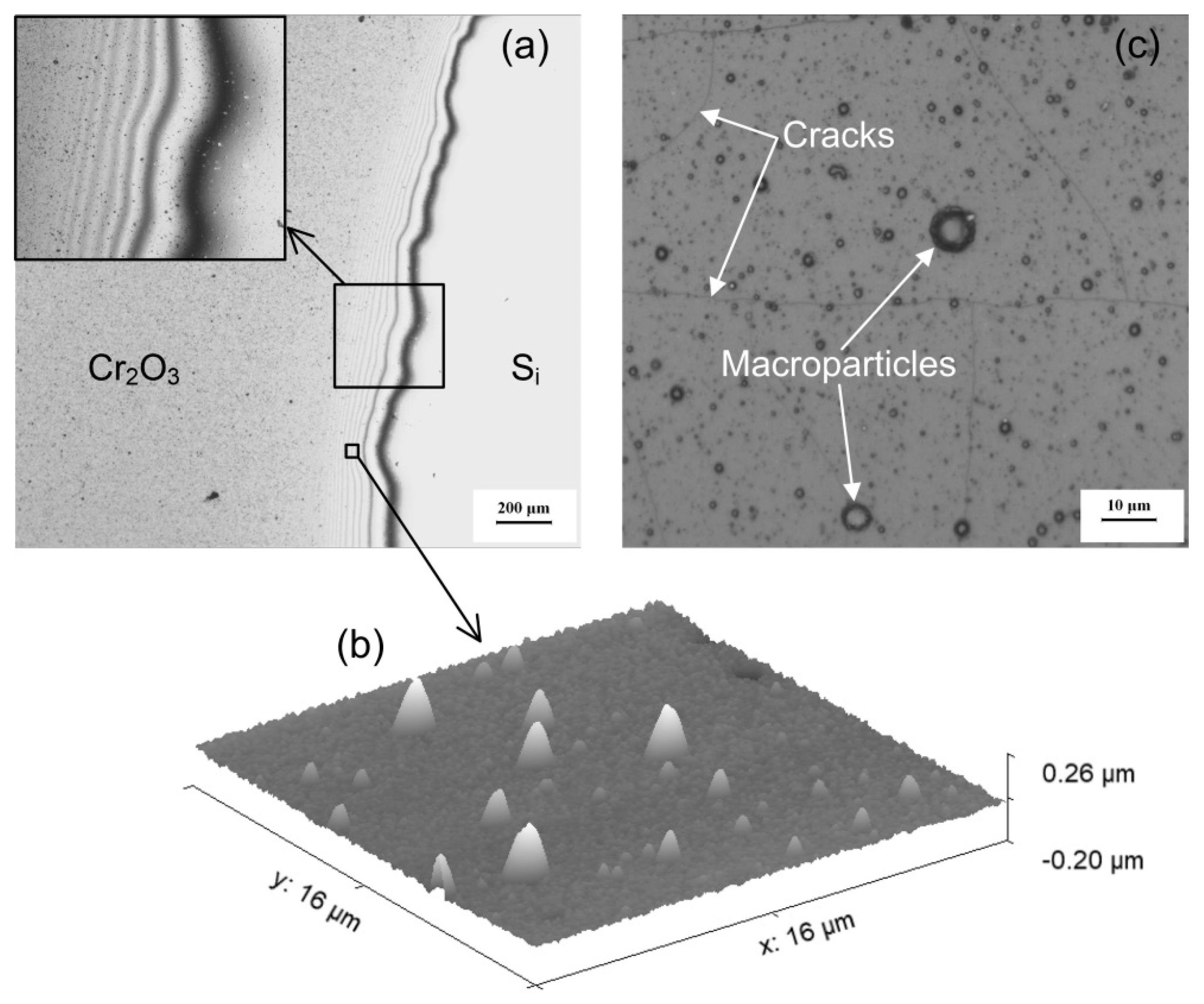
2.1. Cr2O3 Coating Material

The Cr2O3 coating was deposited on the silicon wafer through arc ion plating [25]. By controlling the deposition time, coating thickness was controlled to be about 3.5 μm. The temperature was 300 °C during the deposition process. As observed by the scanning electron microscope (SEM), the columnar grains of Cr2O3 were randomly arranged along the thickness direction, and the cross-sectional shape of the columnar grains was polygonal with an average size of 34.6–38.4 nm. More detailed information about the coating can be found in reference [25].
It can be seen from the optical microscope that the Cr2O3 coating exhibits many interference fringes in the depositional edge zone where the electrode was placed, as shown in Figure 1a. The closer the Cr2O3 coating is to the edge, the clearer the interference fringes are. According to the images obtained by the atomic force microscope at the interference fringes (Figure 1b), there is no step-like mutation in the height of the coating at the interference fringes. Additionally, there are many hill-like macroparticles with different heights and diameters on the surface of the coating. As indicated by the observation results gained by the optical microscope with a higher magnification (Figure 1c), the diameters of the macroparticles range from dozens of nanometers to several micrometers. It can also be seen from Figure 1c that there are many fine cracks on the surface of the coating. These cracks begin to appear about 400 μm away from the depositional edge. The local residual stress was investigated by conducting measurements on the location of the depositional edge and the micro-areas containing large macroparticles and cracks.

2.2. Experimental Test

The micro-Raman spectral information was collected using a Renishaw InVia Reflex laser Raman spectrometer (Wotton-under-Edge, Gloucestershire, UK), with a 532 nm laser, backscattering, 50× objective lens, 2400 lines/mm grating, a laser spot diameter of less than 2 μm on the sample surface, and a spectral resolution smaller than 1 cm−1. The automatic line mapping function of the instrument was applied to conduct the measurement. In the depositional edge zone, the measurement was conducted from the silicon substrate along the direction perpendicular to the interference fringes. The measurement step size was 2 μm in the area densely distributed with interference fringes. After measuring for a length of 150 μm, the step size was changed to 10 μm, and another 150 μm was measured (there were no cracks in the whole measuring area). For the micro-area with the large macroparticle, with the macroparticle as the center, a length of 40 μm was measured at a step size of 2 μm. Similarly, for the micro-area with a crack, at a step size of 2 μm and with the crack as the center, a length of 40 μm was measured along the direction perpendicular to the crack.
The thickness of the Cr2O3 coating in the depositional edge zone was obtained using a Bruker DektakXT profilometer (Karlsruhe, Baden-Württemberg, Germany).

3. Results and Discussions

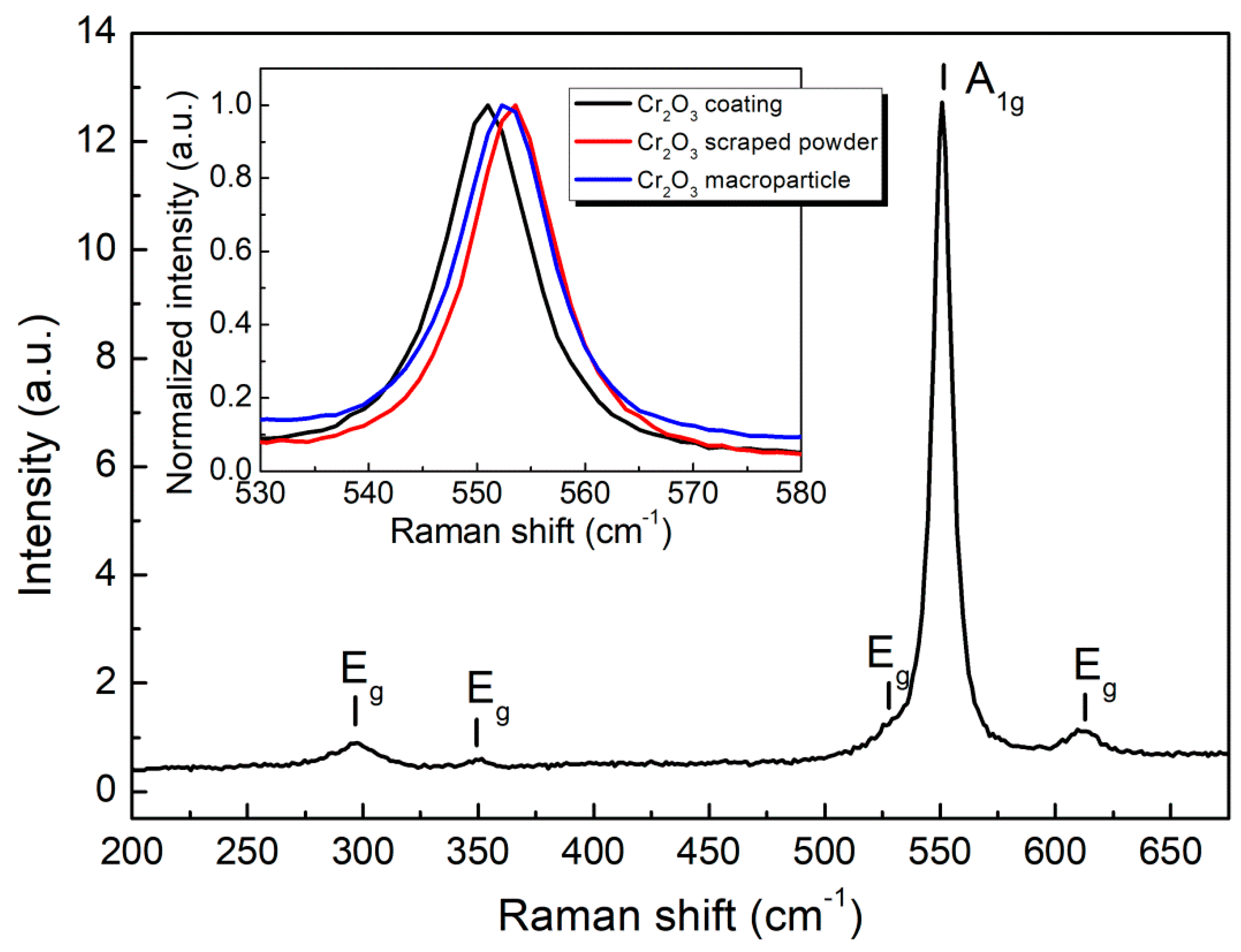
3.1. Raman Peaks of the Cr2O3 Coating

The typical Raman spectrum of the Cr2O3 coating measured in the experiment is shown in Figure 2. Cr2O3 has four Eg modes (~296 cm−1, ~350 cm−1, ~525 cm−1, and ~612 cm−1) and one A1g mode (~551 cm−1), which is consistent with the measurement results in reference [26,27,28]. Based on the measurements, the Raman spectrum of the large macroparticles on the surface of the coating also had the same Raman mode, indicating that the large macroparticles were Cr2O3 aggregates. Among all the peaks of Cr2O3, the A1g mode corresponded to the strongest peak, so it was used in this study to analyze stress. To determine the Raman peak position of the zero-stress state, the Raman spectrum of the Cr2O3 powder scraped off from the coating was measured. The average peak position of the A1g mode of the powder obtained through Lorentz fitting was about 553 cm−1, which is consistent with the results calculated in reference [27,29]. Hence, 553 cm−1 was used as the unstressed reference peak position of the A1g mode in this study. The illustration in Figure 2 shows the comparison of the Raman A1g mode of powder scraped off the Cr2O3 coating and the Raman A1g mode of Cr2O3 macroparticles on the surface of the coating, as well as its comparison with the A1g mode of the coating. It was found that, compared with the powder scraped off the coating, the A1g mode of the Cr2O3 macroparticles on the surface of the coating was significantly wider on the left side, which may have been caused by the presence of more defects in the Cr2O3 macroparticles [30].

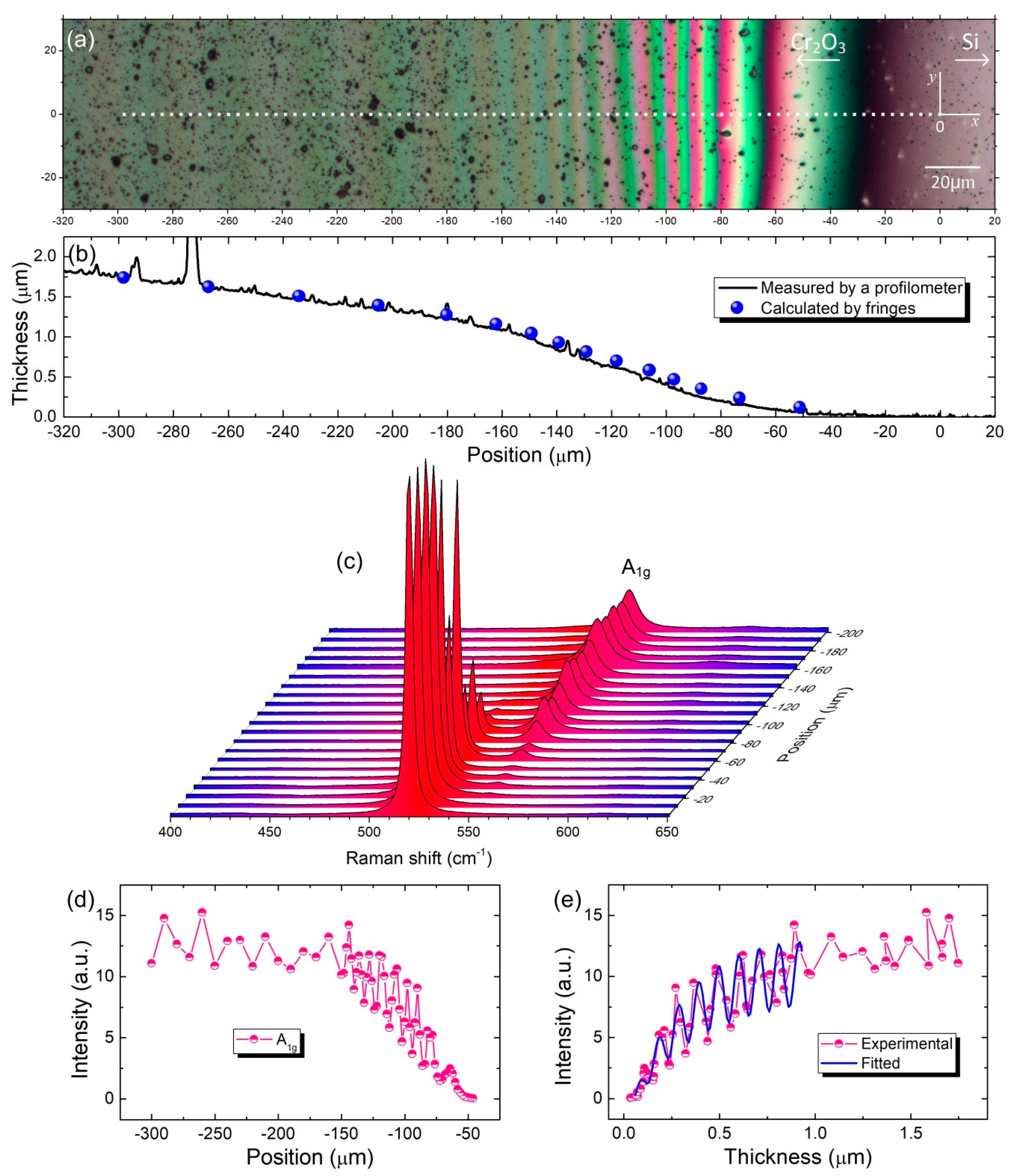
3.2. Thickness of Coatings in the Depositional Edge Zone and Penetration Depth of the Raman Spectrum

The interference fringes in the depositional edge zone observed by the eyepiece of the optical microscope were colored, as shown in Figure 3a, which was a result of equal thickness interference produced by the white light for illumination on the upper and lower surfaces of the Cr2O3 coating. The difference in thickness between the coatings, corresponding to the adjacent interference fringes, was calculated using the following equation:
Δ h = λ 2 n ,
where λ is the wavelength of light and n is the refractive index of the light with a wavelength of λ in Cr2O3. For example, with a yellow light wavelength (λ) of 589 nm and a refractive index (n) of 2.551 [31], the calculated result was about 0.1154 μm. Based on this, the thickness of the Cr2O3 coating at any level of the interference fringes could be determined. Considering that the center of the interference fringe corresponding to yellow light was at the junction of the red fringe and the green fringe, the thickness of the Cr2O3 coating was calculated as shown by the blue sphere in Figure 3b. The discovered thickness was in good agreement with the coating thickness measured by the profilometer (solid black line in Figure 3b), indicating that sparse interference fringes corresponded to slowly varying thicknesses, while dense ones corresponded to rapidly varying thicknesses. The farther from the edge of the coating, the more blurred the interference fringes, because as the coating gets thicker, the light reaching the lower surface of the coating and the light reflected by the lower surface decreases in intensity.
The penetration depth of the Raman spectrum in the Cr2O3 coating could be inferred from the coating thickness and the variation of the Raman peak intensity at different positions of the coating. Figure 3c shows the morphology of the Raman spectrum at different locations in the depositional edge zone. From the edge to the inside of the Cr2O3 coating, the intensity of the 520 cm−1 peak of the substrate single crystal silicon was gradually reduced, while the intensity of the A1g peak of the Cr2O3 coating gradually increased. Figure 3d shows how the intensity of the A1g peak changes specifically with its position. Since the intensity of the A1g peak at the edge was too small to be fitted, it is not shown here. After about −46 μm, the intensity of the A1g peak gradually increased. Figure 3e shows the variation of the intensity of the Raman peak with coating thickness. The high order of the interference indicated a relevant intensity of reflected light. Therefore, the Raman signal of the Cr2O3 layer needs to consider the multiple reflections inside the layer. The effect on the Raman signal of films due to multiple reflections has been addressed by Wang et al. [32] and Camerlingo et al. [33]. Considering the attenuation effect and the multiple reflection effect at the interface, the Raman scattering intensity of the Cr2O3 coating can be fitted by the following Equation (2). The detailed derivation process can be found in reference [33].
I | t 1 1 r 1 r 2 e 2 h ( b + i γ ) | 2 { 1 e 4 b h 4 b + 1 e 2 b h b e b h [ Re ( r 2 ) cos ( 2 γ h ) + Im ( r 2 ) sin ( 2 γ h ) ] + e 4 b h | r 2 | 2 h }
where
t 1 = 2 n 0 n 0 + n 1 + i k 1 ,   r 1 = n 0 n 1 i k 1 n 0 + n 1 + i k 1 ,   r 2 = n 1 + i k 1 n 2 i k 2 n 1 + i k 1 + n 2 + i k 2 ,   b = 2 π k 1 λ ,   γ = 2 π n 1 λ
n 0 = 1 is the refractive index of the light in the air, n 1 and k 1 denote the real and imaginary parts of the complex refractive index of the light in Cr2O3, respectively, and n 2 and k 2 indicate the real and imaginary parts of the complex refractive index of the light in the substrate, respectively. Equation (2) was obtained by assuming that the variation of the complex refractive index of the light in Cr2O3 with λ was negligible, when the wavelength of Raman scattered light (λ ≈ 548 nm) was considered instead of that of the laser (λ = 532 nm). After Equation (3) was substituted into Equation (2), Equation (2) was used to fit the variation of the intensity of the Raman peak with coating thickness. We used n 1 , k 1 , n 2 , k 2 and the scale amplitude of signal intensity as free fitting parameters, obtaining k 1 0.073 . We only fitted the data of the small step Raman measurement area due to the dense data points. The corresponding laser penetration depth was λ / ( 4 π k 1 ) 0.58   μ m . The penetration depth discovered was consistent with the penetration depth (~0.6 μm) of a 632.817nm He-Ne laser in a Cr2O3 coating reported in reference [26], and the penetration depth (0.5 μm) of a 514.5-nm argon ion laser in a Cr2O3 coating reported in reference [27].

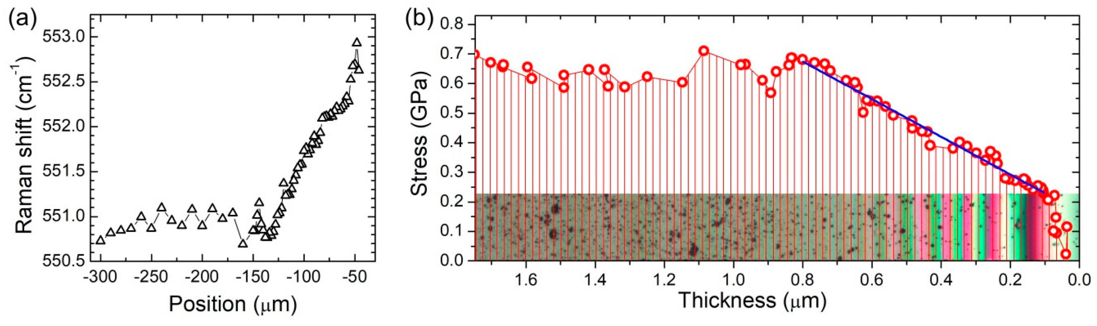
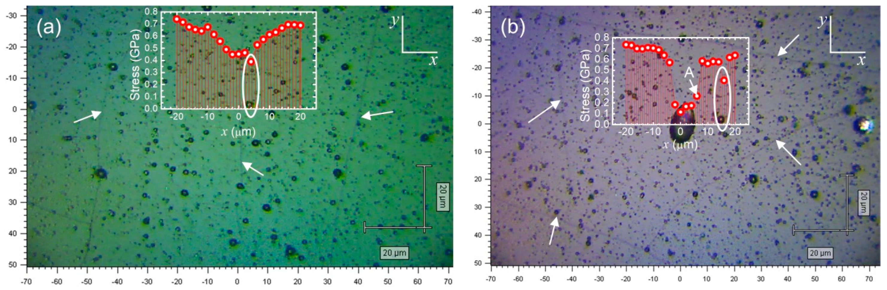
3.3. Residual Stress Analysis in the Local Micro-Area

The variation of the Raman shift of the A1g peak in the depositional edge zone with the position is shown in Figure 4a. From the figure, the Raman shift moved to a low wave number within −132 μm (corresponding to a thickness of 0.8 μm of the Cr2O3 coating), as the change was quite slight. Δ w ( = w w 0 , w is the experimentally obtained Raman shift with stress, and w 0 is the unstressed Raman shift), the Raman shift change of the A1g peak, was used to infer the corresponding stress. The relationship between stress and Δ w can be expressed by the following equation [28,34]:
σ = Δ w × 0.307 ± 0.005   ( GPa ) ,
where the unit of Δ w is cm−1. Thus, when Δ w was positive, the stress was compressive stress, and when Δ w was negative, it was tensile stress. The above equation represents the stress-Raman shift calibration relationship established under the application of hydrostatic pressure. The column microstructures in the thickness direction of the samples we used allowed us to consider the biaxial stress state within the thin layer of the laser test. To apply this calibration relationship in a biaxial stress state, the following three conditions must be met [27,28,34]:
  • The size of the Cr2O3 crystalline grains should be smaller than that of the laser spot. In our experiment, the size of the Cr2O3 crystalline grains (34.6–38.4 nm) was much smaller than that of the laser spot (2 μm).
  • The crystalline grains should be arbitrarily oriented. In our experiment, the Cr2O3 crystalline grains were randomly arranged in the measurement plane.
  • There should be no stress gradient in the thickness of the Cr2O3 coating penetrated by the laser. Huntz et al. [8] demonstrated that the stress gradient in the Cr2O3 coating is negligible. In addition, if there was a noticeable stress gradient in the Cr2O3 coating, a corresponding noticeable broadening of the peaks in Raman spectra was to be expected. In all our experiments, the A1g peaks used were narrow, and there was no noticeable broadening compared with the peaks of powder samples (see inserts in Figure 2), which suggested that the stress gradient was weak.
Because the above three conditions did not seem to impose sufficient limits, the relational expression between stress and Raman shift was used in this study (Equation (4)). With w 0 = 553 cm−1, previously obtained by the powder sample test, we calculated the variation of stress in the depositional edge zone with coating thickness, as shown in Figure 4b. It should be noted that the calculated residual stress σ is one half of the sum of two components, σ x x and σ y y , i.e., σ = 0 . 5 ( σ x x + σ y y ) [35]. Due to the random arrangement of the Cr2O3 crystalline grains in the measurement plane, we considered that the residual stress in the depositional edge zone was equibiaxial, i.e., σ = σ x x = σ y y . According to the figure, the residual stress was tensile; when the thickness of the Cr2O3 coating was less than 0.8 μm, the residual stress increased as the coating thickness increased, and when the thickness of the Cr2O3 coating was greater than 0.8 μm, the residual stress was stable between 0.55 GPa and 0.75 GPa, which is consistent with the measurement results in reference [26]. Specifically, for the thickness in the range of 0.1–0.8 μm, the residual stress increased linearly with the thickness, at a rate of 0.637 GPa/μm. It is worth noting that since the depth for analysis is less than 0.92 μm, the determined stress only involved the upper layer of the coating when the thickness of the coating was greater than 0.92 μm.
Thermal residual stress caused by a mismatch in the thermal expansion coefficient is one of the main sources of residual stress [7]. In this experiment, the thermal expansion coefficient of the silicon substrate was smaller than that of the Cr2O3 coating. During the cooling process, after the high-temperature deposition of the coating, the silicon substrate with less shrinkage limited the shrinkage of the Cr2O3 coating, thereby introducing tensile thermal residual stress in the coating. This thermal residual stress could be calculated based on the following equation [36]:
σ t h = E C O Δ T ( γ S U γ C O ) 1 ν C O ,
where Δ T = T f T i ( T f and T i stand for the final and initial temperatures), γ S U and γ C O denote the expansion coefficients of the substrate and coating, respectively, and E C O and ν C O represent the Young’s modulus and Poisson’s ratio of the coating, respectively. The parameters measured in reference were used to estimate the thermal residual stress in the Cr2O3 coating. The expansion coefficient of Cr2O3, γ C O , = 7.85 × 10⁻⁶ K−1 [37], the expansion coefficient of silicon, γ S U = 2.56 × 10⁻⁶ K−1 [38], the Young’s modulus and Poisson’s ratio of Cr2O3 are E C O = 314 GPa and ν C O = 0.28 [8], and ∆T = (293.15 − 573.15) K = −280 K, so the calculated σ t h was 0.65 GPa. This value accounted for almost all of the residual stress in the Cr2O3 coating measured experimentally in this study, indicating that the contribution to residual stress made by growth stress was negligible, which is consistent with the measurement results obtained in reference [8]. Therefore, the tensile residual stress measured in the Cr2O3 coating could be attributed to the following factor: the thermal expansion coefficient of the silicon substrate was smaller than that of the Cr2O3 coating. The tensile residual stress was the cause of cracks on the surface of the coating. Furthermore, the property of the thermal residual stress that we measured was opposed to the thermal residual stress measured in reference [8] and reference [26], as the thermal expansion coefficient of the metal substrate they used was greater than that of the Cr2O3 coating.
The tensile residual stress measured was the in-plane stress that was perpendicular to the thickness of the coating. This stress led to a decrease in the lattice constant along the thickness direction of the coating due to Poisson contraction, agreeing with the measurement results in reference [25]. Through XRD-based measurement, reference [25] found that the lattice constant of the Cr2O3 coating, prepared using the same method, was smaller than the reference value of the standard lattice constant; additionally, the value they obtained was exactly equal to the lattice constant along the thickness direction. This was similar to the finding that “the tensile in-plane stress measured by the curvature method agrees with the compressive out-of-plane strain measured by XRD”, mentioned in reference [14].
The Raman shifts of the micro-area with Cr2O3 macroparticles and the micro-area with a crack were also obtained, and the stress obtained according to Equation (4) is shown in Figure 5. In the area with a high mutation of the Cr2O3 macroparticle edge, the stress was at an incomplete biaxial stress state, but the stress value was still given based on Equation (4) to correlate the stress measurements in the central area of the macroparticle and the surrounding coatings. However, the stress obtained from these localized areas is not used in the follow-up discussion. At the edges of macroparticles and cracks, the stress in the coating was not equibiaxial. For the crack edge, if the crack penetrated the coating completely along the thickness direction, the stress at the crack edge was expected to be σ y y / 2 , i.e., in the range of 0.275–0.375 GPa (it can be assumed that the σ x x at the crack edge approached zero, while σ y y was almost unaffected). However, the measured stress at the crack edge (about 0.45 GPa) was larger than these values, as shown in Figure 5a, indicating that the crack did not penetrate the entire coating thickness and that σ x x was not completely released. The stress gradually increased with larger distance from the crack, until the equibiaxial stress state was restored. For the macroparticle area, except point A on the right side of the macroparticle (Figure 5b), the measured stress in the coating ranged from 0.55 GPa to 0.75 GPa, indicating that the region with a non-equibiaxial stress state around the macroparticle was very small. In other words, the effect of the Cr2O3 macroparticle on the residual stress in the coating of its surrounding area was very small. This conclusion was further confirmed by the fact that the residual stresses on both sides of the smaller Cr2O3 macroparticles were equivalent (marked by the hollow ellipse in Figure 5). The stress towards the top of Cr2O3 macroparticle was relatively small, indicating that the Cr2O3 macroparticles on the Cr2O3 coating were less affected by the silicon substrate during the process when the coating was prepared and cooled to room temperature.

4. Conclusions

In this study, the thickness of the depositional edge zone of a Cr2O3 coating on a silicon substrate was measured, and the variation of residual stress with thickness was explored. The thickness of the coating was calculated based on the fringes observed in the depositional edge zone and was exactly the same as the thickness measured using a profilometer. The Raman spectrum information in this area was collected, and the penetration depth of a 532 nm laser in the Cr2O3 coating was determined according to variation of intensity of the Raman spectrum. The relationship between the residual stress and the coating thickness was established according to the Raman shift. Based on the data, it was found that there was in-plane tensile residual stress on the Cr2O3 coating, which is a major cause for the formation of microcracks on the coating surface. In the depositional edge zone, towards the inside of the coating from the edge, the coating thickness gradually increased. When the coating thickness was less than 0.8 μm, the residual stress was directly related to the thickness. Conversely, when the thickness was greater than 0.8 μm, the residual stress was stable in the range of 0.55–0.75 GPa. Moreover, the residual stresses in the micro-area with cracks and the micro-area with Cr2O3 macroparticles were also measured. It was discovered that the effect of Cr2O3 macroparticles on the residual stress in the coating of the surrounding area was very small. The residual stress was only partially released at the crack.

Author Contributions

Conceptualization, Q.L.; Investigation, Q.L., Q.Y. and L.W.; Methodology, Q.L.; Project administration, Q.L. and T.G.; Resources, Q.L., T.-G.W. and T.G.; Validation, Q.L., Y.G., Q.Y. and L.W.; Writing—original draft, Q.L. and Y.G.; Writing—review & editing, T.-G.W. and T.G.

Funding

This research was funded by the National Natural Science Foundation of China (No. 11772227 and No. 11772223), the Science and Technology Special Commissioner Program of Tianjin (No. 18JCTPJC64500), the Tianjin Major Science and Technology Project of Military-Civil Integration (No. 18ZXJMTG00050), and the Science Research and Development Foundation of Tianjin University of Technology and Education (No. KJ1809). This research was also partially supported by the University of Delaware Research Foundation.

Acknowledgments

We acknowledge Darren Wu for editing the grammar of the paper.

Conflicts of Interest

The authors declare no conflict of interest.

References

  1. Pang, X.; Gao, K.; Luo, F.; Yang, H.; Qiao, L.; Wang, Y.; Volinsky, A.A. Annealing effects on microstructure and mechanical properties of chromium oxide coatings. Thin Solid Film. 2008, 516, 4685–4689. [Google Scholar] [CrossRef]
  2. Mohammadtaheri, M.; Yang, Q.; Li, Y.; Corona-Gomez, J. The effect of deposition parameters on the structure and mechanical properties of chromium oxide coatings deposited by reactive magnetron sputtering. Coatings 2018, 8, 111. [Google Scholar] [CrossRef]
  3. Huang, K.; Li, L.; Wang, L.; Li, G.; Xu, Y. Effect of DC bias and RF self-bias on the structure and properties of chromium oxide coatings prepared by vacuum cathodic arc deposition. Vacuum 2019, 164, 325–331. [Google Scholar] [CrossRef]
  4. Lodesani, A.; Picone, A.; Brambilla, A.; Giannotti, D.; Jagadeesh, M.S.; Calloni, A.; Bussetti, G.; Berti, G.; Zani, M.; Finazzi, M.; et al. Graphene as an Ideal Buffer Layer for the Growth of High-Quality Ultrathin Cr2O3 Layers on Ni (111). ACS Nano 2019, 13, 4361–4367. [Google Scholar] [CrossRef] [PubMed]
  5. Hou, P.Y.; Ager, J.; Mougin, J.; Galerie, A. Limitations and advantages of Raman spectroscopy for the determination of oxidation stresses. Oxid. Met. 2011, 75, 229–245. [Google Scholar] [CrossRef]
  6. Sebastiani, M.; Bemporad, E.; Carassiti, F. On the influence of residual stress on nano-mechanical characterization of thin coatings. J. Nanosci. Nanotechnol. 2011, 11, 8864–8872. [Google Scholar] [CrossRef] [PubMed]
  7. Withers, P.J.; Bhadeshia, H.K.D.H. Residual stress. Part 2–Nature and origins. Mater. Sci. Technol. 2001, 17, 366–375. [Google Scholar] [CrossRef]
  8. Huntz, A.M.; Piant, A.; Lebrun, J.L.; Daghigh, S. Evidence of stress relaxation in thermally grown oxide layers-experiments and modelling. Mater. Sci. Eng. A-Struct. Mater. Prop. Microstruct. Process. 1998, 248, 44–55. [Google Scholar] [CrossRef]
  9. Goedjen, J.G.; Stout, J.H.; Guob, Q.; Shores, D.A. Evaluation of stresses in Ni-NiO and Cr-Cr2O3 during high temperature oxidation by in situ X-ray diffraction. Mater. Sci. Eng. A-Struct. Mater. Prop. Microstruct. Process. 1994, 177, 115–124. [Google Scholar] [CrossRef]
  10. Tanaka, M.; Kitazawa, R.; Tomimatsu, T.; Liu, Y.F.; Kagawa, Y. Residual stress measurement of an EB-PVD Y2O3-ZrO2 thermal barrier coating by micro-Raman spectroscopy. Surf. Coat. Technol. 2009, 204, 657–660. [Google Scholar] [CrossRef]
  11. Xu, K.W.; He, J.W. Microstrain-induced additional peak shift and method for determining macrostress in plasma-assisted CVD coatings. Surf. Coat. Technol. 1994, 70, 115–120. [Google Scholar] [CrossRef]
  12. Jäger, N.; Klima, S.; Hruby, H.; Julin, J.; Burghammer, M.; Keckes, J.F.; Mitterer, C.; Daniel, R. Evolution of structure and residual stress of a fcc/hex-AlCrN multi-layered system upon thermal loading revealed by cross-sectional X-ray nano-diffraction. Acta Mater. 2019, 162, 55–66. [Google Scholar] [CrossRef]
  13. Gilardi, E.; Fluri, A.; Lippert, T.; Pergolesi, D. Real-time monitoring of stress evolution during thin film growth by in situ substrate curvature measurement. J. Appl. Phys. 2019, 125, 082513. [Google Scholar] [CrossRef]
  14. Fluri, A.; Pergolesi, D.; Roddatis, V.; Wokaun, A.; Lippert, T. In situ stress observation in oxide films and how tensile stress influences oxygen ion conduction. Nat. Commun. 2016, 7, 10692. [Google Scholar] [CrossRef] [Green Version]
  15. Fluri, A.; Pergolesi, D.; Wokaun, A.; Lippert, T. Stress generation and evolution in oxide heteroepitaxy. Phys. Rev. B 2018, 97, 125412. [Google Scholar] [CrossRef] [Green Version]
  16. Stoney, G.G. The tension of metallic films deposited by electrolysis. Proc. R. Soc. Lond. Ser. A Contain. Pap. Math. Phys. Character 1909, 82, 172–175. [Google Scholar] [CrossRef] [Green Version]
  17. Schöngrundner, R.; Treml, R.; Antretter, T.; Kozic, D.; Ecker, W.; Kiener, D.; Brunner, R. Critical assessment of the determination of residual stress profiles in thin films by means of the ion beam layer removal method. Thin Solid Film. 2014, 564, 321–330. [Google Scholar] [CrossRef] [Green Version]
  18. Bolelli, G.; Righi, M.G.; Mughal, M.Z.; Moscatelli, R.; Ligabue, O.; Antolotti, N.; Sebastiani, M.; Lusvarghi, L.; Bemporad, E. Damage progression in thermal barrier coating systems during thermal cycling: A nano-mechanical assessment. Mater. Des. 2019, 166, 107615. [Google Scholar] [CrossRef]
  19. Tao, S.; Liang, B.; Ding, C.; Liao, H.; Coddet, C. Wear characteristics of plasma-sprayed nanostructured yttria partially stabilized zirconia coatings. J. Therm. Spray Technol. 2005, 14, 518–523. [Google Scholar] [CrossRef]
  20. Salvati, E.; Romano-Brandt, L.; Mughal, M.Z.; Sebastiani, M.; Korsunsky, A.M. Generalised residual stress depth profiling at the nanoscale using focused ion beam milling. J. Mech. Phys. Solids 2019, 125, 488–501. [Google Scholar] [CrossRef]
  21. Qiu, W.; Kang, Y.L. Mechanical behavior study of microdevice and nanomaterials by Raman spectroscopy: A review. Chin. Sci. Bull. 2014, 59, 2811–2824. [Google Scholar] [CrossRef]
  22. Kang, Y.; Qiu, Y.; Lei, Z.; Hu, M. An application of Raman spectroscopy on the measurement of residual stress in porous silicon. Opt. Lasers Eng. 2005, 43, 847–855. [Google Scholar] [CrossRef]
  23. Qiu, W.; Cheng, C.L.; Liang, R.R.; Zhao, C.W.; Lei, Z.K.; Zhao, Y.C.; Ma, L.L.; Xu, J.; Fang, H.J.; Kang, Y.L. Measurement of residual stress in a multi-layer semiconductor heterostructure by micro-Raman spectroscopy. Acta Mech. Sin. 2016, 32, 805–812. [Google Scholar] [CrossRef]
  24. Kemdehoundja, M.; Grosseau-Poussard, J.L.; Dinhut, J.F. Raman microprobe spectroscopy measurements of residual stress distribution along blisters in Cr2O3 thin films. Appl. Surf. Sci. 2010, 256, 2719–2725. [Google Scholar] [CrossRef]
  25. Wang, T.G.; Jeong, D.; Kim, S.H.; Wang, Q.; Shin, D.W.; Melin, S.; Iyengar, S.; Kim, K.H. Study on nanocrystalline Cr2O3 films deposited by arc ion plating: I. composition, morphology, and microstructure analysis. Surf. Coat. Technol. 2012, 206, 2629–2637. [Google Scholar] [CrossRef]
  26. Kemdehoundja, M.; Dinhut, J.F.; Grosseau-Poussard, J.L.; Jeannin, M. High temperature oxidation of Ni70Cr30 alloy: Determination of oxidation kinetics and stress evolution in chromia layers by Raman spectroscopy. Mater. Sci. Eng. A-Struct. Mater. Prop. Microstruct. Process. 2006, 435, 666–671. [Google Scholar] [CrossRef]
  27. Birnie, J.; Craggs, C.; Gardiner, D.J.; Graves, P.R. Ex situ and in situ determination of stress distributions in chromium oxide films by Raman microscopy. Corros. Sci. 1992, 33, 1–12. [Google Scholar] [CrossRef]
  28. Mougin, J.; Le Bihan, T.; Lucazeau, G. High-pressure study of Cr2O3 obtained by high-temperature oxidation by X-ray diffraction and Raman spectroscopy. J. Phys. Chem. Solids 2001, 62, 553–563. [Google Scholar] [CrossRef]
  29. Calvarin, G.; Huntz, A.M.; Le Goff, A.H.; Joiret, S.; Bernard, M.C. Oxide scale stress determination by Raman spectroscopy application to the NiCr/Cr2O3 system and influence of yttrium. Scr. Mater. 1998, 38, 1649–1658. [Google Scholar] [CrossRef]
  30. Sahoo, S.; Sharma, G.L.; Katiyar, R.S. Raman spectroscopy to probe residual stress in ZnO nanowire. J. Raman Spectrosc. 2012, 43, 72–75. [Google Scholar] [CrossRef]
  31. Weast, R.C.; Astle, M.J.; Beyer, W.H. CRC Handbook of Chemistry and Physics, 69th ed.; CRC press: Boca Raton, FL, USA, 1988. [Google Scholar]
  32. Wang, Y.Y.; Ni, Z.H.; Shen, Z.X.; Wang, H.M.; Wu, Y.H. Interference enhancement of Raman signal of graphene. Appl. Phys. Lett. 2008, 92, 043121. [Google Scholar] [CrossRef]
  33. Camerlingo, C.; Lisitskiy, M.P.; De Stefano, L.; Rea, I.; Delfino, I.; Lepore, M. Evaluation of thin metal film thickness from light attenuation and multi-reflection effects on micro-Raman response. Thin Solid Film. 2013, 536, 142–146. [Google Scholar] [CrossRef]
  34. Mougin, J. Tenue mécanique de couches d’oxyde thermiques générées sur le chrome et sur quelques aciers inoxydables ferritiques: Étude des contraintes et de d’adhérence. Ph.D. Thesis, INP, Grenoble, France, 3 July 2001. [Google Scholar]
  35. Tolpygo, V.K.; Clarke, D.R. Spalling failure of α-alumina films grown by oxidation: I. Dependence on cooling rate and metal thickness. Mater. Sci. Eng. A-Struct. Mater. Prop. Microstruct. Process. 2000, 278, 142–150. [Google Scholar] [CrossRef]
  36. Sarrazin, P.; Galerie, A.; Fouletier, J. Les Mécanismes de la Corrosion Sèche: Une Approche Cinétique; EDP Sciences: Paris, France, 2000. [Google Scholar]
  37. Kudielka, H. Die thermische Ausdehnung der isotypen Mischreihen-Endglieder Cr2O3 und α-Al3O2, ermittelt mit einer neuen, lichtstarken Seemann–Bohlin-Kammer. Mon. für Chem. Chem. Mon. 1972, 103, 72–80. [Google Scholar] [CrossRef]
  38. Becker, P.; Seyfried, P.; Siegert, H. The lattice parameter of highly pure silicon single crystals. Z. für Phys. B Condens. Matter 1982, 48, 17–21. [Google Scholar] [CrossRef]
Figure 1. (a) Microscope image showing the morphology of the depositional edge zone of the Cr2O3 coating; (b) Atomic force microscope image showing the morphology of the depositional edge zone of the Cr2O3 coating; and (c) Microscope image showing macroparticles and cracks on the surface of the Cr2O3 coating.
Coatings 09 00500 g001
Figure 2. Raman spectrum of the Cr2O3 coating. The inserts show amplified A1g modes of the coating (black line), the scraped powder (red line) and Cr2O3 macroparticles on the surface of the coating (blue line).
Coatings 09 00500 g002
Figure 3. (a) Optical microscope images of the depositional edge zone of the Cr2O3 coating, with the white dashed line indicating the position scanned by the Raman line; (b) Variation of coating thickness with the position in the depositional edge zone, where the solid black line denotes the results measured by the profilometer and the blue sphere denotes the results calculated according to the series of the interference fringes; (c) Variation of intensity of the Raman peak with the position in the depositional edge zone; (d) Variation of integral intensity of the A1g mode of Cr2O3 with position; (e) Variation of integral intensity of the A1g mode with the thickness of the Cr2O3 coating (circle) and the fitted curve by Equation (2) (blue line).
Coatings 09 00500 g003
Figure 4. Variation of Raman shift and stress in the depositional edge zone of the Cr2O3 coating. (a) Variation of Raman shift with the measurement position; (b) Variation of residual stress with coating thickness.
Coatings 09 00500 g004
Figure 5. Distribution of residual stress in the micro-area with a crack (a) and the micro-area with Cr2O3 macroparticles (b). The white arrows indicate the position of the cracks.
Coatings 09 00500 g005

