Article

Influence of Sputtering Power on the Electrical Properties of In-Sn-Zn Oxide Thin Films Deposited by High Power Impulse Magnetron Sputtering

1
School of Space Science and Physics, Shandong Provincial Key Laboratory of Optical Astronomy and Solar-Terrestrial Environment, Shandong University at Weihai, Weihai 264209, China
2
Shenzhen Key Laboratory of Quantum Science and Engineering, Southern University of Science and Technology, Shenzhen 518055, China
3
Department of Materials Engineering and Center for Plasma and Thin Film Technologies, Ming Chi University of Technology, Taipei 243, Taiwan
4
College of Engineering, Chang Gung University, Taoyuan 333, Taiwan
5
Department of Mechanical Engineering, National Taiwan University, Taipei 106, Taiwan
6
The Key Lab of Guangdong for Modern Surface Engineering Technology, National Engineering Laboratory for Modern Materials Surface Engineering Technology, Guangdong Institute of New Materials, Guangzhou 510651, China
*
Authors to whom correspondence should be addressed.
Coatings 2019, 9(11), 715; https://doi.org/10.3390/coatings9110715
Submission received: 28 September 2019 / Revised: 28 October 2019 / Accepted: 29 October 2019 / Published: 31 October 2019
(This article belongs to the Special Issue Magnetron Sputtering Deposited Thin Films and Its Applications)

Abstract

:
In-Sn-Zn oxide (ITZO) thin films have been studied as a potential material in flat panel displays due to their high carrier concentration and high mobility. In the current work, ITZO thin films were deposited on glass substrates by high-power impulse magnetron sputtering (HiPIMS) at room temperature. The influence of the sputtering power on the microstructures and electrical performance of ITZO thin films was investigated. The results show that ITZO thin films prepared by HiPIMS were dense and smooth. There were slight variations in the composition of ITZO thin films deposited at different sputtering powers. With the sputtering power increasing from 100 W to 400 W, the film’s crystallinity was enhanced. When the sputtering power was 400 W, an In2O3 (104) plane could be detected. Films with optimal electrical properties were produced at a sputtering power of 300 W, a carrier mobility of 31.25 cm2·V−1·s−1, a carrier concentration of 9.11 × 1018 cm−3, and a resistivity of 2.19 × 10⁻⁴ Ω·m.

1. Introduction

Transparent conducting oxides (TCOs) have recently received much attention because of several of their advantages, such as high transmittance in the visible light range, good chemical stability, good electrical conductivity, compatibility, and adhesion to typical glass substrates [1,2,3]. Because of their unique and excellent properties, they have been adopted in numerous applications. Flat panel displays, energy-efficient windows, transparent semiconductor components (thin film transistors and memories), solar cells, and organic light emitting diodes are some of the application examples of TCOs [4,5,6]. Nowadays, in order to satisfy demand for a constantly updated display technique, issues regarding the smoothness, optical, and electrical properties of TCOs are attracting immense attention [7].
Recently, significant interest has emerged around oxide semiconductor film materials which can be applied in optoelectronic devices, such as panel displays and solar cells. These kinds of materials can possess excellent optical and electrical properties [8,9,10,11]. One material in particular, indium-tin-zinc oxide (ITZO), has received attention because of its high carrier mobility and high carrier concentration [12]. The bottom of the conduction band of ITZO is composed of In5s and Sn5s orbitals, which are divergent and symmetrical. The direct spatial overlap of these orbitals is beneficial to the carrier transportation [13]. Besides this, the substitution of In3+ ions by Zn2+/Sn4+ pairs leads to lattice distortion, the existence of ZnIn (i.e. the substitution of In3+ by Zn2+) is beneficial in forming VO (oxygen vacancies), and SnIn (i.e. the substitution of In3+ by Sn4+) donor defects, which improve the carrier concentration [14,15].
Spin coating [16,17] and magnetron sputtering [18,19] are the most widely used technologies for the fabrication of ITZO thin films. Of the various magnetron sputtering methods, high-power impulse magnetron sputtering (HiPIMS) is superior for the preparation of oxide films [20,21,22] due to its higher ionization degree of the sputtered species [23,24]. Thin films grown by this process feature a dense, smooth, and uniform surface [25,26]. Rezek et al. successfully prepared indium-gallium-zinc-oxide (IGZO) thin films with high optical and electrical properties using HiPIMS technology in 2018 [27]. They found that strong target peak power density could result in the formation of a very dense structure with reduced defect content, which leads to an increase in carrier movement and Hall mobility. It is therefore reasonable to expect that ITZO thin films with enhanced electrical properties can be achieved through the HiPIMS deposition method. In the current work, the influence of sputtering power on the microstructural and electrical properties of ITZO thin films was investigated.

2. Materials and Methods

ITZO thin films were deposited on glass and silicon substrates (7 mm × 7 mm) by HiPIMS using a ceramic ITZO target (99.9% purity, Φ76.2 mm, In:Sn:Zn:O = 18.46:10.77:10.77:60.00 at %, Zhongnuoxincai (Beijing) Technology Co., Ltd., Beijing, China) at room temperature. The deposition system (MGS-500, Junsun Tech. Co., Ltd., New Taipei) as shown in Figure 1) was pre-pumped to a base pressure below 7 × 10⁻⁴ Pa. The working pressure and Ar (purity of 99.99%) flow rate were maintained at 0.7 Pa and 20 mL/min, respectively. The magnetron was fabricated by Junsun Tech. Co., Ltd. and the target was powered by SPIK2000A pulse supply (Shen Chang Electric Co., New Taipei) with a constant power of 300 W. The pulse on-time (ton) and the pulse off-time (toff) were 50 μs and 500 μs, respectively. The duty cycle, which is defined as the ratio between the ton and the sum of ton plus toff, was maintained at 9.09% during the deposition. One-hundred-nanometer-thick ITZO thin films were prepared at different sputtering powers of 100, 200, 300, and 400 W.
I-V characteristics of HiPIMS power output were monitored using an oscilloscope (Rigol DS5202CA, Rigol Technologies. Inc., Beijing, China). The films’ thicknesses were measured using a step profiler (KosakaSurfcoder, Kosaka Laboratory Ltd., Tokyo, Japan). The chemical compositions were analyzed by an electron probe X-ray microanalyzer (EPMA, JEOL JXA-8200, JEOL, Tokyo, Japan). The phase structure was characterized using an X-ray diffractometer (XRD, X’Pert PRO MPD, Philips PANalytical Almelo, Netherlands). The films’ morphology and roughness were observed using a field emission scanning electron microscope (FE-SEM, JEOL JSM-6701F, JEOL, Tokyo, Japan) and via atomic force microscopy (AFM, DI-Dimension 3100, Digital Instruments, Bresso, Italy), respectively. The films’ electrical properties were obtained using a Hall effect measurement system (AHM-800B, Agilent Technologies, Santa Clare, CA, USA).

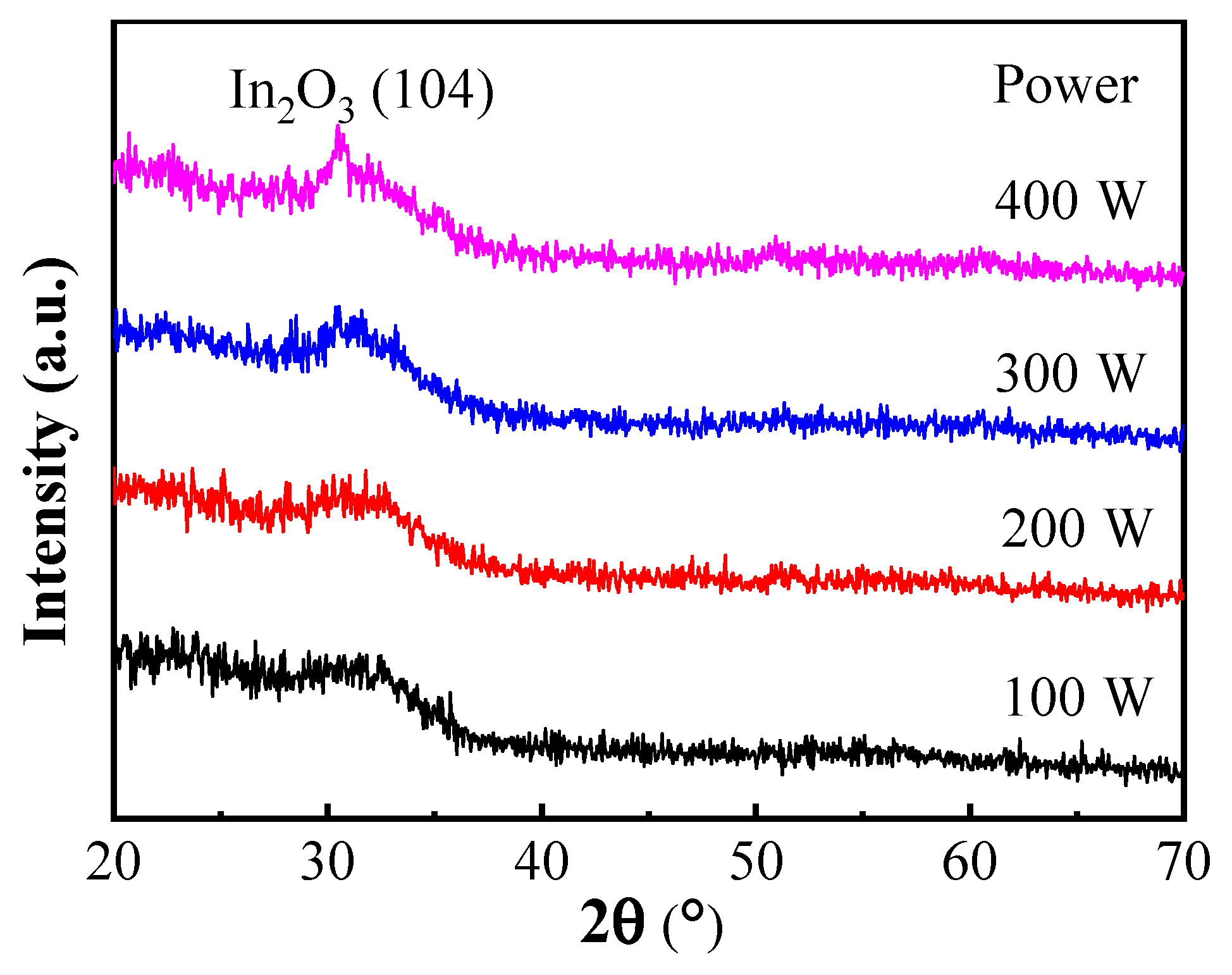
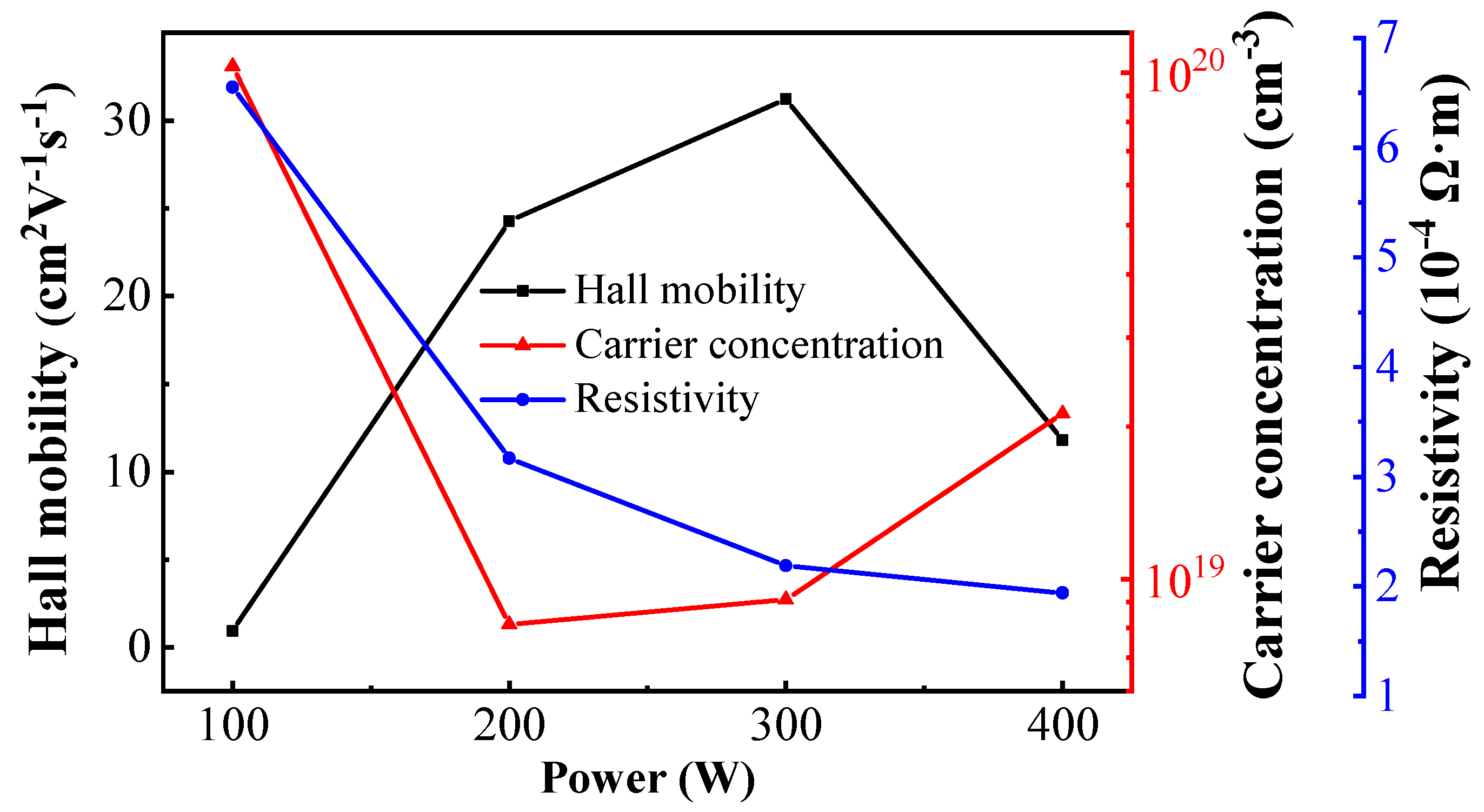
3. Results and Discussion

ITZO thin films were deposited by HiPIMS with a duty cycle of 9.09%. Figure 2 shows the target current and voltage under different sputtering powers. The peak power densities are calculated and compared in Figure 3. When the sputtering power increases from 100 to 400 W, the instantaneous target peak current increases, resulting in the target peak power density rising from 50.0 to 270.1 W·cm−2. The improvement in the deposition rate is due to the enhanced sputtering power providing more energy to Ar ionization, which causes more atoms to be sputtered from the target.
Table 1 shows the relationship between the sputtering power and the film’s composition. With an increase in sputtering power, the concentration of In, Sn, Zn, and O changes slightly. The results indicate that the sputtering power does not much affect the atomic concentration of ITZO thin films deposited by HiPIMS. Meanwhile, all the films are oxygen deficient, under which condition oxygen vacancies are easily formed, contributing to the film’s conductivity.
An X-ray diffractogram of the ITZO thin films fabricated at various sputtering powers is shown in Figure 4. For the ITZO thin films deposited at sputtering powers between 100 and 300 W, there is no obvious diffraction peak that can be detected, indicating the amorphous nature of the films. As the sputtering power increases to 400 W, a crystallization peak emerges at around 30.97° (JCPDS: 22-0336), which we believe comes from In2O3 (104). As detected by EPMA analysis, In content is much higher than that of Sn and Zn. As the sputtering power increases, the atom migration ability is enhanced and In2O3 tends to precipitate to form a crystal phase. As a result, the crystallinity of the ITZO thin films improves [28,29]. It has been reported that post-annealing can further enhance the film’s crystallinity [30]. However, considering the heat resistivity of the flexible substrate where ITZO is potentially used in the flexible display, we did not conduct this experiment in this work.
FE-SEM analyses were performed to obtain the top surface appearance of ITZO thin films. The observations at a magnification of 2 × 10⁵ are shown in Figure 5. From the SEM images, we can see that ITZO thin films prepared using HiPIMS technology are uniform and smooth. With the sputtering power increasing from 100 to 400 W, the films become more homogeneous, and their roughness decreases from 2.10 to 1.18 nm. Compared with the published ITZO films [31], the grain size of ITZO thin films deposited by HiPIMS is smaller and the films are more uniform and denser, which would be beneficial for avoiding carrier losses and defect states in ITZO-based devices [32].
The films’ electrical properties including Hall mobility and carrier concentration were measured and are shown in Figure 6. With sputtering power increasing from 100 to 300 W, high-energy particles have more energy to migrate and diffuse on the film’s surface and thus the film’s quality improves [33], i.e. the denser structure ensures the smooth transfer of the carriers and enhances the film’s carrier mobility [34]. As a result, the Hall mobility rises significantly from 0.93 to 31.25 cm2·V−1·s−1 with the sputtering power increase. However, an obvious decrease in Hall mobility can be observed when the sputtering power rises further to 400 W. We believe that the formation of In2O3 increases the grain boundary scattering and reduces the carrier mobility [35]. A similar phenomenon has also been reported in ITZO:N films [36].
As for the carrier concentration, when the sputtering power is 100 W, the crystallinity of ITZO films deposited by the low-energy sputtered particles is relatively poor, resulting in large numbers of defects (such as oxygen vacancies) in the films [27]. The film’s carrier concentration reaches a high value of 1.03 × 1020 cm−3 at this sputtering power. With the sputtering power increasing to 200 W, the increment in the oxygen amount reduces the oxygen vacancy (VO) content, while the reduced Sn amount lowers the substitution of In by Sn (SnIn). The decrement in those donor defects of VO and SnIn leads to a significant decrease in the carrier concentration to 8.13 × 1018 cm−3. In addition, the decrease in Zn content also makes it harder to from donor defects such as VO and SnIn due to the presence of ZnIn lowering the formation energy of VO and SnIn [7]. Upon further increasing the sputtering power to 300 W, the Zn content remains almost unchanged while O content slightly decreases and Sn content rises a little, resulting in the donor defects of VO and SnIn increasing moderately. The carrier concentration then increases marginally to 9.11 × 1018 cm−3.
As the sputtering power reaches 400 W, the higher sputtering power is conducive to the ionization of the working gas Ar [14,37,38], which could transfer sufficient energy to the sputtering species (In, Sn, and Zn atoms or clusters) and improve their activity. This causes ZnIn, SnIn, and VO to form easily, enhancing the carrier concentration (ZnIn lowering the formation energy of SnIn and VO, while SnIn and VO are the donor defects in ITZO films). On the other hand, In, Sn, and Zn species with higher activity easily react with oxygen, leading to increased oxygen content, which reduces the number of VO defects. Under the combined effect of the above two conflicting factors, the carrier concentration further increases to 2.12 × 1019 cm−3.
The variation in the films’ resistivity is influenced by the Hall mobility and carrier concentration, as shown in Equation (1) [34], i.e.
ρ = 1 ( e × N × μ )
where ρ is the film’s resistivity, e is the electron charge, N is the carrier concentration, and μ is the Hall mobility. According to Figure 6, resistivity values of ITZO thin films decrease with increasing sputtering power. For the films deposited at sputtering powers of 100, 200, 300, and 400 W, their resistivities are 6.55 × 10⁻⁴, 3.17 × 10⁻⁴, 2.19 × 10⁻⁴, and 1.94 × 10⁻⁴ Ω·m, respectively.

4. Conclusions

In this work, ITZO thin films were deposited at different sputtering powers using HiPIMS technology. The microstructures and electrical properties of the films were investigated. The results showed that all the films were uniform with dense structures. As the sputtering power increased, the deposition rates of the ITZO films rose and the film’s composition altered slightly. The film’s Hall mobility peaked at 31.25 cm2·V−1·s−1 when the sputtering power was 300 W. This is a relatively high carrier mobility compared to the ITZO films deposited by other technologies and is a very important feature for improving the response speed of the switch. The corresponding film’s carrier concentration and resistivity were found to be 9.11 × 1018 cm−3 and 2.19 × 10⁻⁴ Ω·m, respectively. This result is attributable to highly ionized plasma, which leads to improved film quality and excellent electrical properties. Overall, ITZO thin films deposited by HiPIMS have been found to have superior uniformity and higher carrier mobility, with increased response speed and reduced power consumption, which we expect will improve the performance of devices incorporating ITZO films.

Author Contributions

Conceived and designed the experiments, S.-C.C. and H.S.; performed the experiments, Z.-Y.L. and Q.-H.H.; analyzed the data, M.-J.D. and S.-S.L.; contributed reagents/materials/analysis tools, M.-H.L. and T.-L.Y.

Funding

This work was supported by the Shandong Province Natural Science Foundation (ZR2018QEM002), the Key Lab of Guangdong for Modern Surface Engineering Technology (2018KFKT04), the Ministry of Science and Technology of Taiwan (no. 107-2221-E-131-036), and the Young Scholars Program of Shandong University, Weihai.

Acknowledgments

We also thank H.C. Lin and C.Y. Kao of the Instrumentation Center, National Taiwan University for their assistance with the EPMA experiments.

Conflicts of Interest

The authors declare no conflict of interest.

References

  1. Politano, G.G.; Vena, C.; Desiderio, G.; Versace, C. Spectroscopic ellipsometry investigation of the optical properties of graphene oxide dip-coated on magnetron sputtered gold thin films. J. Appl. Phys. 2018, 123, 055303. [Google Scholar] [CrossRef]
  2. Solis-Cortes, D.; Schrebler, R.; Navarrete-Astorga, E.; Lopez-Escalante, M.; Martin, F.; Ramos-Barrado, J.R.; Dalchiele, E.A. Electrochemical characterization of transparent conducting IZO:Ga thin films. J. Alloy. Compd. 2019, 808, 151776. [Google Scholar] [CrossRef]
  3. Kim, S.H.; Yoon, J.; Jin, S.H.; Bang, J.; Song, P. Stabilizing of Mechanical property of amorphous In-Zn-O thin films with hydrogen flow. Coatings 2019, 9, 485. [Google Scholar] [CrossRef]
  4. Granqvist, C.G. Transparent conductors as solar energy materials: A panoramic review. Sol. Energy Mater. Sol. Cells 2007, 91, 1529–1598. [Google Scholar] [CrossRef]
  5. Li, Z.Y.; Lu, Y.B.; Zhao, J.F.; Song, S.M.; Yang, B.B.; Xin, Y.Q.; Wang, K.L.; Yang, T.L. Fabrication and the electrical and optical properties of nitrogen-doped In-Sn-Zn oxide thin-film transistors. Chin. J. Lumin. 2017, 38, 1622–1628. [Google Scholar]
  6. Leterrier, Y.; Medico, L.; Demarco, F.; Manson, J.A.E.; Betz, U.; Escola, M.F.; Olsson, M.K.; Atamny, F. Mechanical integrity of transparent conductive oxide films for flexible polymer-based displays. Thin Solid Film. 2004, 460, 156–166. [Google Scholar] [CrossRef]
  7. Sahu, B.B.; Long, W.; Han, J.G. Highly conductive flexible ultra thin ITO nanoclusters prepared by 3-D confined magnetron sputtering at a low temperature. Scr. Mater. 2018, 149, 98–102. [Google Scholar] [CrossRef]
  8. Park, J.; Kim, Y.S.; Kim, J.H.; Park, K.; Park, Y.C.; Kim, H.S. The effects of active layer thickness and annealing conditions on the electrical performance of ZnON thin-film transistors. J. Alloy. Compd. 2016, 688, 666–671. [Google Scholar] [CrossRef]
  9. Weimer, P.K. The TFT- a new thin-film transistor. Proc. Inst. Radio Eng. 1962, 50, 1462–1469. [Google Scholar] [CrossRef]
  10. Lan, L.F.; Zhang, P.; Peng, J.B. Research progress on oxide-based thin film transistors. Acta Phys. Sin. 2016, 65, 128504. [Google Scholar]
  11. Sun, H.; Chen, S.C.; Peng, W.C.; Wen, C.K.; Wang, X.; Chuang, T.H. The influence of oxygen flow ratio on the optoelectronic properties of p-type Ni1-xO films deposited by ion beam assisted sputtering. Coatings 2018, 8, 168. [Google Scholar] [CrossRef]
  12. Choi, P.; Lee, J.; Park, H.; Baek, D.; Lee, J.; Yi, J.; Kim, S.; Choi, B. Fabrication and characteristics of high mobility InSnZnO thin film transistors. J. Nanosci. Nanotechnol. 2016, 16, 4788–4791. [Google Scholar] [CrossRef] [PubMed]
  13. Nguyen, C.P.T.; Trinh, T.T.; Raja, J.; Le, A.H.T.; Lee, Y.J.; Dao, V.A.; Yi, J. Source/Drain metallization effects on the specific contact resistance of indium tin zinc oxide thin film transistors. Mater. Sci. Semicond. Process. 2015, 39, 649–653. [Google Scholar] [CrossRef]
  14. Lu, Y.B.; Yang, T.L.; Ling, Z.C.; Cong, W.Y.; Zhang, P.; Li, Y.H.; Xin, Y.Q. How does the multiple constituent affect the carrier generation and charge transport in multicomponent TCOs of In-Zn-Sn oxide. J. Mater. Chem. C 2015, 3, 7727–7737. [Google Scholar] [CrossRef]
  15. Li, Z.Y.; Yang, H.Z.; Chen, S.C.; Lu, Y.B.; Xin, Y.Q.; Yang, T.L.; Sun, H. Impact of active layer thickness of nitrogen-doped In-Sn-Zn-O films on materials and thin filmtransistor performances. J. Phys. D Appl. Phys. 2018, 51, 175101. [Google Scholar] [CrossRef]
  16. Jin, C.H.; You, I.K.; Kim, H.K. Effect of rapid thermal annealing on the properties of spin-coated In-Zn-Sn-O films. Curr. Appl. Phys. 2013, 13, S177–S181. [Google Scholar] [CrossRef]
  17. Lee, D.M.; Kim, J.K.; Hao, J.C.; Kim, H.K.; Yoon, J.S.; Lee, J.M. Effects of annealing and plasma treatment on the electrical and optical properties of spin-coated ITZO films. J. Alloy. Compd. 2014, 583, 535–538. [Google Scholar] [CrossRef]
  18. Damisih, I.; Ma, H.C.; Finanda, F.; Kim, J.J.; Lee, H.Y. Effect of composition in transparent conducting indium Zinc Tin Oxide thin films deposited by RF magnetron sputtering. J. Nanoelectron. Optoelectron. 2012, 7, 483–487. [Google Scholar] [CrossRef]
  19. Kwon, S.H.; Jung, J.H.; Cheong, W.S.; Lee, G.H.; Song, P.K. Dependence of electrical and mechanical durability on Zn content and heat treatment for co-sputtered ITZO films. Curr. Appl. Phys. 2012, 12, S59–S63. [Google Scholar] [CrossRef]
  20. Anders, A. Tutorial: Reactive high power impulse magnetron sputtering (R-HiPIMS). J. Appl. Phys. 2017, 121, 171101. [Google Scholar] [CrossRef] [Green Version]
  21. Vlcek, J.; Rezek, J.; Houska, J.; Cerstvy, R.; Bugyi, R. Process stabilization and a significant enhancement of the deposition rate in reactive high-power impulse magnetron sputtering of ZrO2 and Ta2O5 films. Surf. Coat. Technol. 2013, 236, 550–556. [Google Scholar] [CrossRef]
  22. Wu, C.H.; Yang, F.C.; Chen, W.C.; Chang, C.L. Influence of oxygen/argon reaction gas ratio on optical and electrical characteristics of amorphous IGZO thin films coated by HiPIMS process. Surf. Coat. Technol. 2016, 303, 209–214. [Google Scholar] [CrossRef]
  23. Sun, H.; Chen, S.C.; Wen, C.K.; Chuang, T.H.; Yazdi, M.A.P.; Sanchette, F.; Billard, A. P-type cuprous oxide thin films with high conductivity deposited by high power impulse magnetron sputtering. Ceram. Int. 2017, 43, 6214–6220. [Google Scholar] [CrossRef]
  24. Sun, H.; Wen, C.K.; Chen, S.C.; Chuang, T.H.; Yazdi, M.A.P.; Sanchette, F.; Billard, A. Microstructures and optoelectronic properties of CuxO films deposited by high-power impulse magnetron sputtering. J. Alloy. Compd. 2016, 688, 672–678. [Google Scholar] [CrossRef]
  25. Ehiasarian, A.P.; Vetushka, A.; Gonzalvo, Y.A.; Safran, G.; Szekely, L.; Barna, P.B. Influence of high power impulse magnetron sputtering plasma ionization on the microstructure of TiN thin films. J. Appl. Phys. 2011, 109, 104314. [Google Scholar] [CrossRef]
  26. West, G.T.; Kelly, P.J.; Bradley, J.W. A Comparison of thin silver films grown onto zinc oxide via conventional magnetron sputtering and HiPIMS deposition. IEEE Trans. Plasma Sci. 2010, 38, 3057–3061. [Google Scholar] [CrossRef]
  27. Rezek, J.; Houska, J.; Prochazka, M.; Haviar, S.; Kozak, T.; Baroch, P. In-Ga-Zn-O thin films with tunable optical and electrical properties prepared by high-power impulse magnetron sputtering. Thin Solid Films 2018, 658, 27–32. [Google Scholar] [CrossRef]
  28. Waykar, R.G.; Pawbake, A.S.; Kulkarni, R.R.; Jadhavar, A.A.; Funde, A.M.; Waman, V.S.; Pathan, H.M.; Jadkar, S.R. Influence of RF power on structural, morphology, electrical, composition and optical properties of Al-doped ZnO films deposited by RF magnetron sputtering. J. Mater. Sci. Mater. Electron. 2016, 27, 1134–1143. [Google Scholar] [CrossRef]
  29. Zhang, D.H.; Yang, T.L.; Ma, J.; Wang, Q.P.; Gao, R.W.; Ma, H.L. Preparation of transparent conducting ZnO:Al films on polymer substrates by RF magnetron sputtering. Appl. Surf. Sci. 2000, 158, 43–48. [Google Scholar] [CrossRef]
  30. Quass, M.; Steffen, H.; Hippler, R.; Wulff, H. Investigation of diffusion and crystallization processes in thin ITO films by temperature and time resolved grazing incidence X-ray diffractometry. Surf. Sci. 2003, 540, 337–342. [Google Scholar] [CrossRef]
  31. Tong, Y.; Wang, K.L.; Liu, Y.Y.; Li, Y.H.; Song, S.M.; Yang, T.L. Effects of RF power on structure, morphology and photoelectric properties of ITZO thin films. J. Synth. Cryst. 2015, 44, 2338–2342, 2349. [Google Scholar]
  32. Martins, R.; Barquinha, P.; Pereira, L.; Ferreira, I.; Fortunato, E. Role of order and disorder in covalent semiconductors and ionic oxides used to produce thin film transistors. Appl. Phys. Mater. Sci. Process. 2007, 89, 37–42. [Google Scholar] [CrossRef]
  33. Ruske, F.; Pflug, A.; Sittinger, V.; Werner, W.; Szyszka, B.; Christie, D.J. Reactive deposition of aluminium-doped zinc oxide thin films using high power pulsed magnetron sputtering. Thin Solid Films 2008, 516, 4472–4477. [Google Scholar] [CrossRef]
  34. Chen, S.C.; Huang, S.Y.; Sakalley, S.; Paliwal, A.; Chen, Y.H.; Liao, M.H.; Sun, H.; Biring, S. Optoelectronic properties of Cu3N thin films deposited by reactive magnetron sputtering and its diode rectification characteristics. J. Alloy. Compd. 2019, 789, 428–434. [Google Scholar] [CrossRef]
  35. Cho, S.W.; Yun, M.G.; Ahn, C.H.; Kim, S.H.; Cho, H.K. Bi-layer Channel Structure-Based Oxide Thin-Film Transistors consisting of ZnO and Al-doped ZnO with different Al compositions and stacking sequences. Electron. Mater. Lett. 2015, 11, 198–205. [Google Scholar] [CrossRef]
  36. Junjun, J.; Torigoshi, Y.; Suko, A.; Nakamura, S.I.; Kawashima, E.; Utsuno, F.; Shigesato, Y. Effect of nitrogen addition on the structural, electrical, and optical properties of In-Sn-Zn oxide thin films. Appl. Surf. Sci. 2017, 396, 897–901. [Google Scholar]
  37. Agoston, P.; Erhart, P.; Klein, A.; Albe, K. Geometry, electronic structure and thermodynamic stability of intrinsic point defects in indium oxide. J. Phys. Condens. Matter 2009, 21, 455801. [Google Scholar] [CrossRef]
  38. Yaglioglu, B.; Yeom, H.Y.; Paine, D.C. Crystallization of amorphous In2O3-10 wt % ZnO thin films annealed in air. Appl. Phys. Lett. 2005, 86, 261908. [Google Scholar] [CrossRef]
Figure 1. Schematic of the high-power impulse magnetron sputtering (HiPIMS) deposition system. Legend: ITZO, In-Sn-Zn oxide.
Coatings 09 00715 g001
Figure 2. The sputtering voltage and current at different sputtering powers: (a) 100 W; (b) 200 W; (c) 300 W; (d) 400 W. (Channel CH1 detected the sputtering voltage, channel CH2 detected the sputtering current).
Coatings 09 00715 g002
Figure 3. Peak power density and deposition rate at different sputtering powers.
Coatings 09 00715 g003
Figure 4. XRD patterns of ITZO films deposited at different sputtering powers.
Coatings 09 00715 g004
Figure 5. SEM and atomic force microscopy (AFM) images of ITZO films deposited on silicon substrates at sputtering powers of (a,a1) 100 W and (b,b1) 400 W.
Coatings 09 00715 g005
Figure 6. Electrical properties of ITZO films deposited at different sputtering powers.
Coatings 09 00715 g006
Table 1. Atomic concentration of ITZO films deposited at different sputtering powers.
Power
W
InSnZnO
10052.13 (±0.1) at %4.03 (±0.1) at %1.12 (±0.1) at %42.71 (±0.1) at %
20052.72 (±0.1) at %3.40 (±0.1) at %1.06 (±0.1) at %42.82 (±0.1) at %
30052.91 (±0.1) at %3.56 (±0.1) at %1.03 (±0.1) at %42.50 (±0.1) at %
40051.02 (±0.1) at %4.33 (±0.1) at %1.15 (±0.1) at %43.51 (±0.1) at %

