Article

Simulation of the Inductor Structure to Improve FZ Thermal Fields

1
School of Materials Science and Engineering, Hebei University of Technology, Tianjin 300132, China
2
Zhonghuan Advanced Semiconductor Materials Co., Ltd., Yixing 214200, China
3
Hebei Engineering Laboratory of Photoelectronic Functional Crystals, Hebei University of Technology, Tianjin 300130, China
*
Authors to whom correspondence should be addressed.
Coatings 2023, 13(9), 1565; https://doi.org/10.3390/coatings13091565
Submission received: 21 August 2023 / Revised: 1 September 2023 / Accepted: 3 September 2023 / Published: 7 September 2023

Abstract

:
The floating zone (FZ) is one of the important methods for pulling silicon single crystals, but there are still problems of an unstable thermal field and crystallization difficulties. They will directly affect the growth of single crystals, resulting in defects and even fractures, seriously reducing production efficiency. Based on this, the effect of the modified inductor structure on the FZ thermal field is investigated in this paper. Using COMSOL 6.0 simulation software, 2D and 3D FZ models are established. The inductor steps under the 2D model and the inductor slits under the 3D model are compared to analyze the effects of steps and slits on the 8-inch FZ thermal field and melt flow. The distributions of temperature fields and melt flow in the melting zone under the action of the axial magnetic field are calculated by finite element analysis. The results show that the melt under the introduction of steps in the 2D model and the cross-slit structure in the 3D model is the most stable and favorable for crystal growth, which matches the actual production.

1. Introduction

Zone melting is a crucial method for semiconductor material purification and silicon single-crystal growth because the melting zone is suspended between the polysilicon rods and the silicon single crystal; it is also known as the suspended floating zone (FZ) melting method [1], as shown in Figure 1a. The FZ method uses a high-frequency induction principle and skin collection effect through the coil to realize the local surface heating of polysilicon rods, with the help of the surface tension of the molten silicon and the electromagnetic torus buoyancy. The melting zone is in a state of suspension and then in the specific crystal direction of the seed crystal guidance. The melting zone solidification generates a single crystal. The current FZ technique is a modification of the previous technique, where the inductor hole is enormous, and the melt has no “waist”, which causes the single crystal to grow unstably due to gravity, resulting in defects and fracture [2]. The current FZ technique, also known as the needle-eye technique [3], has a very narrow hole in the center of the inductor to form a skinny “waist” and a small melt [4], as shown in Figure 1b. The principle is to use a high-frequency induction inductor as the heat source, with the feed rod and single crystal above and below the inductor, respectively, and the resulting melt is suspended above the inductor and below the feed rod. The melt is suspended above the inductor and below the feed rod. Compared to the Czochralski (CZ) technique [5], the FZ technique does not require a crucible [6]. The single crystals have shallow oxygen content and low dislocation density [7] and are characterized by high purity and quality, resulting in a significant reduction of impurities in silicon and a high minority carrier lifetime but also higher cost. The semiconductor industry has multiplied in recent years, and the purity of CZ silicon has failed to meet the standards of some materials manufacturing. The production of 8-inch FZ silicon is the current mainstream direction, and FZ silicon single crystals can be used in IGBT, MEMS, high-efficiency solar energy, and image sensors. With the development of precision device technology, reducing costs and producing large-size, high-quality FZ silicon single crystals is imperative.
The FZ technique uses the principle of induction heating [8]; the frequency is generally 2–3 MHz [9], and the high voltage DC input is through the power supply cabinet to the oscillating circuit inside the outer groove of the FZ furnace. Finally, the output high-frequency alternating current will produce an electromagnetic (EM) field near the induction inductor, which is essentially a wave function that changes with time. The feed rod part near the inductor will produce eddy currents, and due to its high purity and high resistance, there will be a large amount of Joule heat, which is induction heating. In this paper, based on the numerical simulation study of the EM field, temperature field, and flow field, the structure of the inductor is improved to improve the thermal field [10].
This calculation was performed using COMSOL large simulation software, which has the advantage of wide applicability. Its calculation principle, in which each introduced physical field has its partial differential equation solution formula, was calculated by establishing the geometry, defining the material, introducing multiple physical fields, setting boundary conditions, dividing the mesh, and coupling multiple physical fields [11].
Before the calculation, we need to analyze the relationship between each physical field of the FZ process [12]. Figure 2 shows that specific process parameters and inductor structures affect the physical fields, and the physical fields are coupled with each other [13]. It can also be seen from the figure that the inductor structure dramatically influences the EM field; this is because changes in the inductor structure affect the distribution of the EM field. A change in the EM field causes a difference in the distribution of force and Joule heat in the melt; it further influences the temperature field and flow field. Based on this, it is important to improve the inductor structure.
For the problems of crystallization difficulties and poor crystal quality in the actual production, in this study, we will improve the temperature field and flow field in the melt, design two kinds of inductors in 2D and 3D, and establish an FZ model to analyze them and come up with a suitable and effective inductor structure to improve the production efficiency.

2. Numerical Model and Calculation Method

We created 2D and 3D models and imported them into COMSOL Multiphysics software. COMSOL is a large-scale advanced numerical simulation software, formerly a MATLAB toolbox [14], and later developed into an independent commercial software. COMSOL is based on the finite element method, which is very suitable for solving partial differential equations and systems of equations. It is rich in preconfigured specialized modules covering various disciplines such as electrical, structural mechanics, fluids, heat transfer, chemical engineering, etc., which can simulate and model any system based on physical fields. It can be used to model and simulate any physical field-based system, providing a graphical user interface (GUI), predefined user interfaces, and associated simulation and analysis tools for typical simulation applications. A wide range of specialized tool modules enable numerical computation in specific research directions. At the same time, a rich set of interfaces allows easy interaction with a wide range of third-party software. COMSOL is a general-purpose software platform for modeling and simulating multi-physical-field problems based on advanced numerical computation methods [15]. There are more than twenty physical field modules. In addition, we can couple any two related physical modules. If the pre-built modules do not meet the requirements, we can also define our partial differential equations (sets) to construct models to solve the problems. There are dozens of sub-modules for users to choose from. In addition, users can also be connected to the software platform through electromagnetism, thermodynamics, and other fields of specialized physical interfaces [16], further expanding the platform’s functionality. The advantages of COMSOL for FZ process simulation are the software’s ability to perform multiphysics field coupling, its good suitability for this study, and the integration of modeling, computation, and post-processing for easy data handling. Figure 3 introduces the basic modules of COMSOL Multiphysics.
Initially, the inductors used in the preparation of single crystals by the FZ method had no steps and secondary slits, only a main slit and a central hole, while later, to better melt polysilicon as well as to adapt to the trajectory of polysilicon melting, beveled surfaces were introduced on the surface of the inductors, and based on the basic understanding of the inductor structure. In the present study, it has been improved.
To compare the effects of inductor steps and slits on the melt, 2D inductors were designed with and without steps, as shown in Figure 4; 3D inductors were designed with one and cross shapes for comparison, and the models are shown in Figure 5. After importing the model to define the material and add physical fields, including a magnetic field (mf), solid and fluid heat transfer (ht), and laminar flow (spf) and after coupling electromagnetic heat (emh), non-isothermal flow (nitf), and Marangoni effect (mar), under the magnetic field module, following Ampere’s law, the relative permeability is chosen for the magnetization model and calculated as follows:
B = μ 0 μ r H
where B is the magnetic induction strength, and H is the magnetic field strength. Assuming that the current flows on the surface [17], the approximation considers the feed rod, melt, and single crystal to be axisymmetric and incorporates rotation under the 3D model, which is more conducive to analyzing the effects of changes in inductor structure, under the heat transfer module, setting the boundary temperature, and the crystallization and melting interface is set to the melting point temperature. This module is coupled with laminar flow, and only the effect of buoyancy is considered due to the slight change in material density. It is easier to converge using the Boussinesq approximation to calculate the non-isothermal flow. Due to the presence of tension gradients (caused by temperature gradients) on the surface of the melt, it is also necessary to include the Marangoni effect for the analysis.
When setting up the grid, due to the complexity of the model, a different grid division is required for each region, and a user-controlled grid, generally a free tetrahedral grid [18], is chosen to refine the grid for the 2D and 3D melt parts, respectively, as shown in Figure 6 and Figure 7. Figure 6 refines the melt mesh and shows the boundary layer refinement due to the apparent solute boundary layer at the growth interface and the powerful free surface interactions (EM forces, Marangoni forces, etc., which will be described below) resulting from flow, so a finer grid is used for the calculation. Figure 7a shows the portion of the melt obscured by the inductor, and we have enlarged the mesh in the part of the melt so that we can better observe it. The finer the grid, the more accurate the calculation. A schematic diagram of the overall structure of the FZ process is given in Figure 7b.

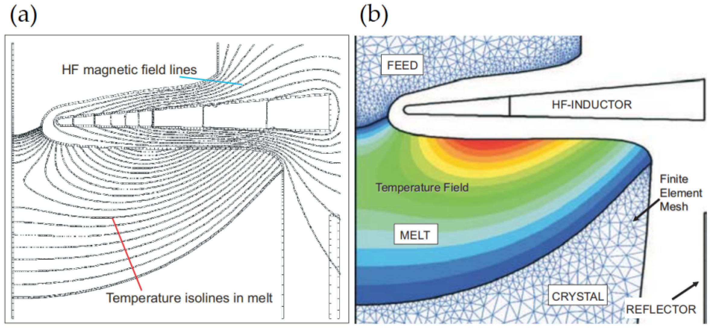
3. Introduction to Physical Fields

3.1. The Electromagnetic Field

The principle of induction heating mentioned is to generate an EM field around the inductor using high-frequency currents and produce a large amount of Joule heat. The calculation of alternating currents at high frequencies is based on the time-harmonic assumption to set the equation:
× μ 0 1 × A + σ V + j ω σ A = J e
where A is the magnetic induction, µ0 is the permeability, σ is the conductivity, V is the potential, j is the imaginary part unit, ω is the angular frequency, and Je is the generated current density.
In the early days, modeling was done using a 2D model, which saved computational time. In the 2D results, the contour line distribution of the magnetic vector potential is shown, as shown in Figure 8a. Due to the simple two-dimensional model, the central magnetic field is reduced. The external electromagnetic field of the silicon is enhanced, generating a high-temperature region at the free surface of the melt, as shown in Figure 8b, which makes the 2D and 3D results fit better [19]. A part of the line is also present inside the inductor, but practically all the line distribution is present between the inductor and the silicon surface [20].
Figure 2 also shows that the EM field and the interface shape are strongly coupled, based on the fact that the surfaces are axisymmetric, but the inductor is asymmetric to the melt during the FZ process. The simulation process requires defining the EM heat source and calculating the EM force. The 3D model is divided into a triangular mesh, as shown in Figure 9a. Based on the skin effect of the current, the current is mainly concentrated on the inductor surface with high surface current density, which contributes to a feed rod. The current flow differs on the silicon surface and in the inductor slit. On the silicon surface, the current flows almost parallel to the inductor. When the current passes through the inductor slit region, it flows vertically upward to the feed rod and single crystal, respectively, so that the density of the EM heat source is minimized in the slit region, as shown in Figure 9b [21]. Therefore, optimizing the inductor slit design can change the current distribution, melt temperature distribution, and flow.

3.2. Melt Temperature and Flow

The EM field distribution determines the melt flow, which is closely related to the temperature distribution, and its temperature distribution should be studied first before studying the flow. Figure 10 shows the temperature distribution of the melt in three dimensions as well as the temperature distribution of the cross-section [22], where a high-temperature gradient is formed in the melt by direct heating of the induction inductor and shows high current density and temperature at the side silt, while the main silt has low current density and temperature, showing an asymmetric temperature field, the temperature field is calculated as follows:
ρ U · ( h ) = · ( a h )
where h is the enthalpy, and a is the diffusivity. The latent heat is calculated as follows:
Q L = ρ V g L
Vg is the local crystal growth rate, and L is the latent heat of silicon. The surface current density distribution in the EM model is coupled to the heat production at the free surface of the melt in the heat transfer model by the following equation:
Q E M = J s 2 δ Q
QEM and Js are the surface power density and the current density at the free surface of the melt. The temperature distribution in the melt is made as uniform as possible in a feed rod and single crystal rotating environment. Figure 11 shows the action of different forces in the melt [23]. Due to the weak penetration of the EM field in the melt part, a transverse shear stress is formed at the free surface boundary of the melt, and this force contains the EM and Marangoni forces [24], and the melt also contains the buoyancy force, which acts on the whole melt. For the temperature field, boundary conditions need to be set, with the melting boundary and the interaction of EM and Marangoni forces as the first and second type of boundary conditions, respectively:
F = F E M + F M a = 1 4 μ 0 δ s ( J s 2 ) + γ T s ( T )
where γ is the surface tension, the Marangoni force is due to the existence of the surface tension gradient. The direct influence on the surface tension gradient in a melt is the temperature gradient. The temperature at the melting and crystallization interface is low, making the Marangoni force to the two ends of the diffusion, which is unfavorable for the melt. The direction of EM force is opposite to it, which requires the control of the magnetic field to weaken the Marangoni effect. Since the single crystal and feed rod are rotating during the FZ process, it makes the angular velocity component in the melt, which is strongly coupled with the warp velocity itself. It affects the melt flow together, while the rotation also inhibits the flow in the warp direction. It can be seen from the figure that the EM, Marangoni, and buoyancy forces form a closed loop in the melt region, and the presence of these forces causes the existence of vortices in the melt. Vortex 3 is caused by the EM force due to the dense magnetic induction lines near it; vortex 1 is caused by the Marangoni and buoyancy forces and is unstable; and vortex 2 is driven by the buoyancy force alone, and the generation of these vortices affects the distribution of RRV, so that when pulling doped single crystals, impurities in the melt flow faster at the vortex, resulting in lower resistivity [25] values in the middle of the two vortices.

4. Proof of Simulation Results

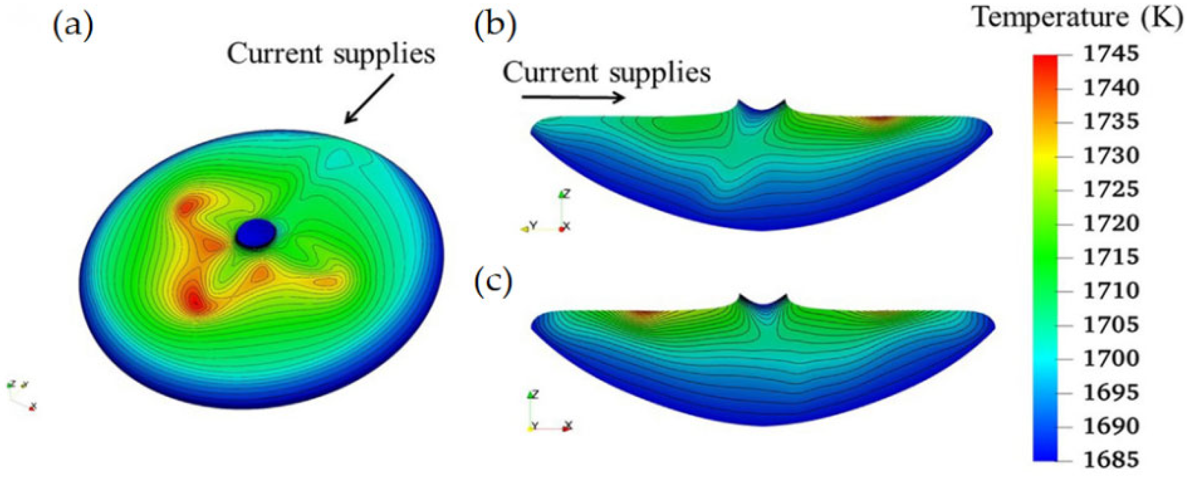
4.1. 2D Model Simulation Results

The simulation results of the 2D model, referring to the Refs. [26,27] were calculated for the melt temperature and flow under stepped and unstepped inductors. Figure 12 shows the melt temperature distribution in the absence and with flow, respectively. Without flow, the inductor steps reduce the temperature at the center of the melt and increase the temperature at the outer diameter of the inductor. To compare the effect of stepped and unstepped inductors more significantly on the melt, it is clear that the temperature in the center of the melt is lower with the addition of flow because the inductor step enhances melt flow.
The increase of steps decreases the gradient of the distribution of the magnetic induction intensity, which makes the difference of the magnetic induction intensity within the polysilicon shrink. By comparing Figure 12c,d, it can be found that the maximum value of the melting zone temperature under the coils with steps is smaller. We have found that the resistivity distribution of the single crystals grown in the single-crystal coils with steps is more even when we conduct single-crystal growth experiments with the two kinds of coils, which is very useful for improving the quality of the single crystals.
To investigate the formation of vortices and their distribution in the melt due to the force, we chose the model with a stepped inductor underneath for convective calculations, time 10 min, frequency 2.5 MHz. We found three vortices in the flow results, as shown in Figure 13, formed by the combined action of EM, buoyancy, and Marangoni forces [28], which are also highly consistent with the results of force distribution in Figure 11. The flow is stronger at the center of the melt and second at the two ends. The reason is that the Marangoni effect dominates at the center and produces the largest vortex [29], while the two ends are close to the inductor, where the magnetic induction strength is high, and the vortex is formed mainly by EM forces. The flow results explain well the difference in temperature distribution in the melt above, and the 2D simulation results prove that the inductor steps greatly influence the thermal field and crystal growth in the melt.

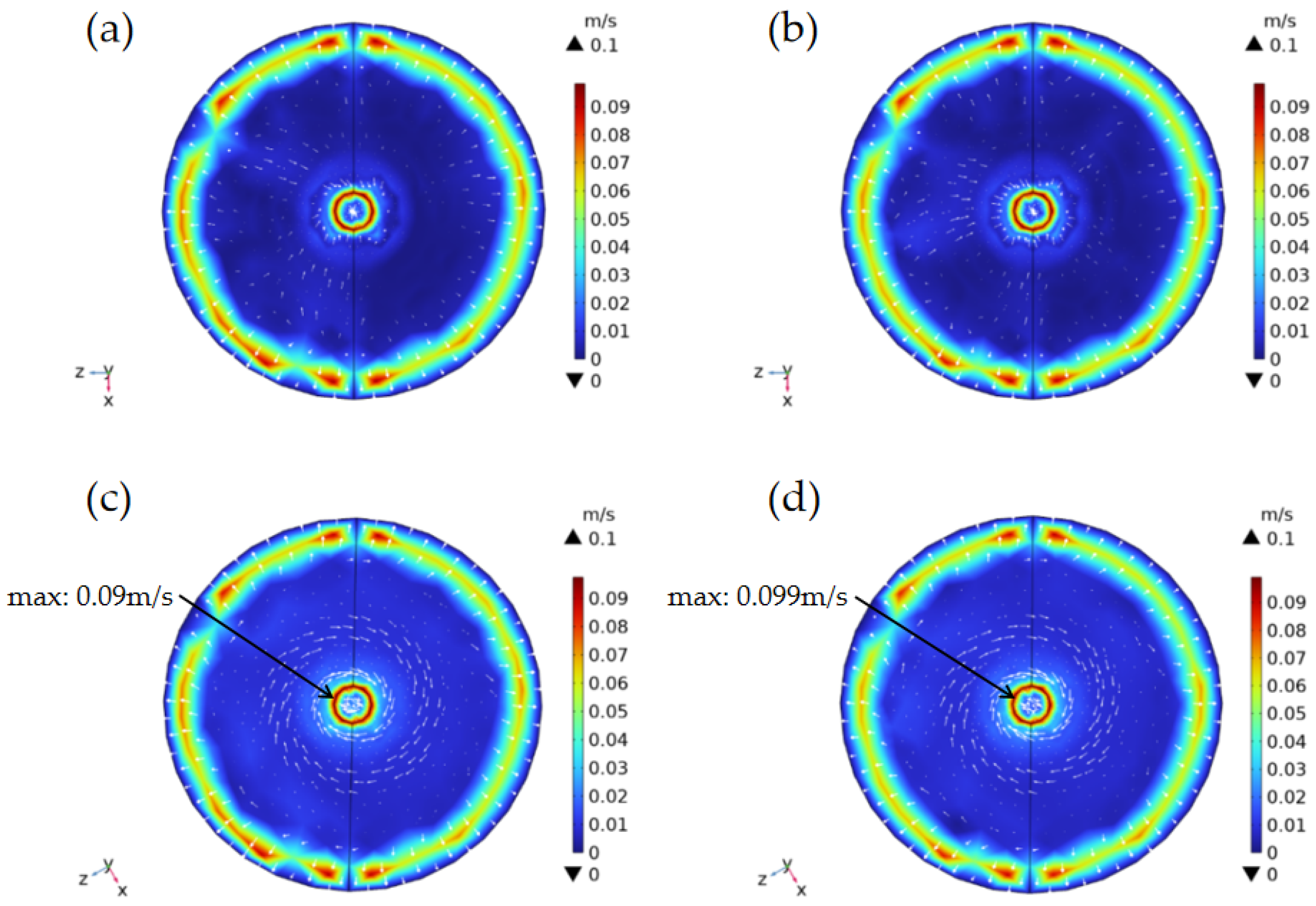
4.2. 3D Model Simulation Results

The 3D results refer to Ref. [30]; Figure 14 shows the current density distribution of two kinds of 3D inductors. The inductor slit changes can directly affect the distribution of the current and the induced magnetic field [31]. It can be seen that the current distribution of the one-way inductor is concentrated in the center around the hole and the slit, the current distribution of the outer side of the current distribution is less; it is because the density of the ring-effect currents is greatest at the inner diameter of the coil, the electromagnetic field generated is most concentrated at the “waist” of the melting zone of the crystals, thus generating the most Joule heat close to the center of the melting surface and the least Joule heat close to the outer surface of the polycrystalline silicon melt, which results in a very uneven distribution of radial temperatures across the entire polycrystalline silicon melt. Thus, the radial temperature distribution across the melting surface of polycrystalline silicon [32] is very uneven. However, the cross-way inductor, due to the existence of more slits, increased current from the main slit into the current shunt so that the current distribution is more uniform. At the same time, the current distribution in the outer side of the current distribution compared to the one-way inductor, the distribution of the current can be a greater degree of the effect of the melt so that the melt of the temperature is more uniformly distributed. The detailed calculation of temperature is mentioned in the following section.
In the following, the effect of the change in inductor structure on the melt temperature distribution. We calculated the temperature distribution of the melt transient for three different cases under two inductors separately. Figure 15 shows the melt temperature distribution for both inductors in the no flow, with flow and flow plus rotation cases, respectively. In the case of no flow, the temperature in both melting zones is mainly concentrated in the main silt, with little transfer to the secondary silt. When flow is added, the temperature distribution becomes relatively uniform and disperses the temperature of the main silt. The current is too concentrated since there is only one slit in the one-way inductor. A large amount of heat is distributed in the central hole and secondary silt during the FZ process. After adding rotation, the temperature is concentrated around the central hole, making the local temperature too high and the radial temperature gradient in the melt too large. To observe the radial temperature of the melt more intuitively, we intercept the radial width of the melt for temperature calculation, as shown in Figure 16, and get that the temperature gradient of the melt under the one-way inductor is larger than that under the cross-way coil, and it is most apparent near the center hole. In Figure 17, we calculated the axial temperature of the waist, measured at a distance of the line connecting the centers of the top and bottom of the “waist”. Figure 17 and Figure 18 show that the high-temperature zone in the “waist” of the one-way inductor is greater, and the axial temperature gradient is large, which will make the “waist” of the melt become very thin or even fracture in actual production.
In contrast, the cross-way inductor has more slits and a large flux density distribution range, which makes the temperature distribution more uniform. There is no heat concentration near the center hole. Therefore, the slit of the inductor directly affects the temperature distribution of the melt and affects the crystal growth.
Figure 19 shows the flow distribution in the melt under both inductors, with the same scale factor for the velocity arrows. It can be found that under the cross inductor, the flow is stronger in all but the outermost part of the melt, the convection in both melts becomes uniform with rotation, and the convection in the melt under the cross-way inductor has a greater maximum value of velocity at the center due to the addition of more slits, which better solves the problem of thermal concentration. The 3D simulation results prove that the inductor slit greatly influences the temperature and flow in the melt, fundamentally due to the different inductor slit designs resulting in different distribution of magnetic induction lines. Based on this, it is proved that the design of the cross-way slit is more advantageous by calculating the thermal and flow fields.

5. Conclusions

The implementation of the FZ process proves that COMSOL can realize the calculation of complex models, covers a wide range of physics, and can realize the coupling calculation of multiple physical fields. This simulation analyzes the thermal and flow fields from two dimensions: 2D steps and 3D slits, and the results are consistent with the actual production situation. The calculation results show that the inductor structure can change the distribution of the EM field, temperature, and melt flow. The temperature and flow in the melt are more uniformly distributed with step inductors and cross-way inductors. The addition of steps decreases the center temperature of the melt zone, and the cross-way slit disperses the temperature of the center hole so that the temperature will not be overly concentrated in the “waist”, and the thermal field becomes more stable.
Meanwhile, after calculating the simulation results, we refer to previous literature studies [33] and compare them to find that under certain growth parameter conditions, the addition of step and cross-way slits does enable the dislocation-free growth of FZ single crystal silicon. Therefore, the study of the effect of the change of growth parameters on the growth of FZ silicon is a problem that needs to be solved in the follow-up work. Meanwhile, the shortcoming of this study is that the modeling process did not include the “Deformation Geometry” module and only considered the influence of the inductor structure on the physical field of the melting zone, thus ignoring the change in the shape of the interface.
Based on the above, the step and cross slits design should be applied to inductors in actual production, making the FZ process more stable and improving the crystal quality. The direct simulation results obtained through numerical modeling were in good agreement with the actual production test. More importantly, using this numerical simulation method can reduce the amount of experimental and deepen the understanding of the FZ silicon single crystal growth system.

Author Contributions

Conceptualization, G.C.; Methodology, G.C.; Software, J.S.; Data curation, G.C.; Writing—original draft, X.A.; Supervision, C.S., H.Z., J.S., L.X., G.L. and G.C. All authors have read and agreed to the published version of the manuscript.

Funding

This work was Funded by the project for the Science and Technology Correspondent of Tianjin City (Grant No. 20YDTPJC01710) and the Research Foundation of Education Bureau of Hebei (Grant No. QN2021044).

Institutional Review Board Statement

Not applicable.

Informed Consent Statement

Not applicable.

Data Availability Statement

Not applicable.

Conflicts of Interest

The authors declare no conflict of interest.

References

  1. Mohamed Ariff, A.H.; Hashmi, M.S.J.; Brabazon, D. Monocrystalline Silicon Grown Using Floating Zone Technique. In Reference Module in Materials Science and Materials Engineering; Elsevier: Amsterdam, The Netherlands, 2018; ISBN 978-0-12-803581-8. [Google Scholar]
  2. Sueoka, K.; Kamiyama, E.; Vanhellemont, J. Theoretical Study of the Impact of Stress on the Behavior of Intrinsic Point Defects in Large-Diameter Defect-Free Si Crystals. J. Cryst. Growth 2013, 363, 97–104. [Google Scholar] [CrossRef]
  3. Ratnieks, G.; Muižnieks, A.; Mühlbauer, A. Modelling of Phase Boundaries for Large Industrial FZ Silicon Crystal Growth with the Needle-Eye Technique. J. Cryst. Growth 2003, 255, 227–240. [Google Scholar] [CrossRef]
  4. Feigelson, R.S. Crystal Growth History: Theory and Melt Growth Processes. J. Cryst. Growth 2022, 594, 126800. [Google Scholar] [CrossRef]
  5. Taishi, T.; Ohno, Y.; Yonenaga, I. Constitutional Supercooling in Heavily As-Doped Czochralski Si Crystal Growth. J. Cryst. Growth 2014, 393, 42–44. [Google Scholar] [CrossRef]
  6. Hossain, M.M.; Watauchi, S.; Nagao, M.; Tanaka, I. Effects of Growth Parameters on Silicon Molten Zone Formed by Infrared Convergent-Heating Floating Zone Method. J. Cryst. Growth 2017, 459, 105–111. [Google Scholar] [CrossRef]
  7. Muižnieks, A.; Raming, G.; Mühlbauer, A.; Virbulis, J.; Hanna, B.; Ammon, W.V. Stress-Induced Dislocation Generation in Large FZ-and CZ-Silicon Single Crystals—Numerical Model and Qualitative Considerations. J. Cryst. Growth 2001, 230, 305–313. [Google Scholar] [CrossRef]
  8. Dold, P. Analysis of Microsegregation in RF-Heated Float Zone Growth of Silicon—Comparison to the Radiation-Heated Process. J. Cryst. Growth 2004, 261, 1–10. [Google Scholar] [CrossRef]
  9. Rost, H.-J.; Menzel, R.; Luedge, A.; Riemann, H. Float-Zone Silicon Crystal Growth at Reduced RF Frequencies. J. Cryst. Growth 2012, 360, 43–46. [Google Scholar] [CrossRef]
  10. Rost, H.-J.; Buchovska, I.; Dadzis, K.; Juda, U.; Renner, M.; Menzel, R. Thermally Stimulated Dislocation Generation in Silicon Crystals Grown by the Float-Zone Method. J. Cryst. Growth 2020, 552, 125842. [Google Scholar] [CrossRef]
  11. Wünscher, M.; Menzel, R.; Riemann, H.; Lüdge, A. Combined 3D and 2.5 D Modeling of the Floating Zone Process with Comsol Multiphysics. J. Cryst. Growth 2014, 385, 100–105. [Google Scholar] [CrossRef]
  12. Rudevičs, A.; Muižnieks, A.; Ratnieks, G.; Mühlbauer, A.; Wetzel, T. Numerical Study of Transient Behaviour of Molten Zone during Industrial FZ Process for Large Silicon Crystal Growth. J. Cryst. Growth 2004, 266, 54–59. [Google Scholar] [CrossRef]
  13. Muiznieks, A.; Virbulis, J.; Lüdge, A.; Riemann, H.; Werner, N. Floating Zone Growth of Silicon. In Handbook of Crystal Growth; Elsevier: Amsterdam, The Netherlands, 2015; pp. 241–279. ISBN 978-0-444-63303-3. [Google Scholar]
  14. Yu, F.; Chen, W.; Zhang, D. The Research of Simulation on Eddy Current Separation Process Based on MATLAB and COMSOL. Procedia CIRP 2016, 56, 520–523. [Google Scholar] [CrossRef]
  15. Han, X.-F.; Kakimoto, K.; Alradi, S.; Zaidat, K. Numerical Investigation of Floating Zone Silicon Using Halbach Array Magnets. J. Cryst. Growth 2020, 546, 125773. [Google Scholar] [CrossRef]
  16. Menzel, R.; Rost, H.-J.; Kießling, F.M.; Sylla, L. Float-Zone Growth of Silicon Crystals Using Large-Area Seeding. J. Cryst. Growth 2019, 515, 32–36. [Google Scholar] [CrossRef]
  17. Han, X.-F.; Liu, X.; Nakano, S.; Harada, H.; Miyamura, Y.; Kakimoto, K. 3D Numerical Simulation of Free Surface Shape during the Crystal Growth of Floating Zone (FZ) Silicon. J. Cryst. Growth 2018, 483, 269–274. [Google Scholar] [CrossRef]
  18. Mühlbauer, A.; Muiznieks, A.; Virbulis, J. Analysis of the Dopant Segregation Effects at the Floating Zone Growth of Large Silicon Crystals. J. Cryst. Growth 1997, 180, 372–380. [Google Scholar] [CrossRef]
  19. Mühlbauer, A.; Muiznieks, A.; Raming, G.; Ratnieks, G. 2D and 3D Numerical Modelling of FZ Large Silicon Single Crystal Growth: Relation between Growth Process and Crystal Quality. In Proceedings of the International Scientific Colloquium Modelling for Saving Resources, Riga, Latvia, 17–18 May 2001; pp. 17–22. [Google Scholar]
  20. Nacke, B.; Muiznieks, A. Numerical Modelling of the Industrial Silicon Single Crystal Growth Processes. GAMM-Mitteilungen 2007, 30, 113–124. [Google Scholar] [CrossRef]
  21. Ratnieks, G.; Muiznieks, A.; Buligins, L.; Raming, G.; Mühlbauer, A.; Lüdge, A.; Riemann, H. Influence of the Three Dimensionality of the HF Electromagnetic Field on Resistivity Variations in Si Single Crystals during FZ Growth. J. Cryst. Growth 2000, 216, 204–219. [Google Scholar] [CrossRef]
  22. Han, X.-F.; Liu, X.; Nakano, S.; Kakimoto, K. Numerical Analysis of Dopant Concentration in 200 Mm (8 Inch) Floating Zone Silicon. J. Cryst. Growth 2020, 545, 125752. [Google Scholar] [CrossRef]
  23. Raming, G.; Muižnieks, A.; Mühlbauer, A. Numerical Investigation of the Influence of EM-Fields on Fluid Motion and Resistivity Distribution during Floating-Zone Growth of Large Silicon Single Crystals. J. Cryst. Growth 2001, 230, 108–117. [Google Scholar] [CrossRef]
  24. Lan, C.W.; Chian, J.H. Three-Dimensional Simulation of Marangoni Flow and Interfaces in Floating-Zone Silicon Crystal Growth. J. Cryst. Growth 2001, 230, 172–180. [Google Scholar] [CrossRef]
  25. Lei, A.; Græsvænge, M.; Hindrichsen, C. Reduced Radial Resistivity Variation of FZ Si Wafers with Advanced NTD. J. Cryst. Growth 2019, 512, 65–68. [Google Scholar] [CrossRef]
  26. Surovovs, K.; Muiznieks, A.; Sabanskis, A.; Virbulis, J. Hydrodynamical Aspects of the Floating Zone Silicon Crystal Growth Process. J. Cryst. Growth 2014, 401, 120–123. [Google Scholar] [CrossRef]
  27. Sabanskis, A.; Virbulis, J. Simulation of the Influence of Gas Flow on Melt Convection and Phase Boundaries in FZ Silicon Single Crystal Growth. J. Cryst. Growth 2015, 417, 51–57. [Google Scholar] [CrossRef]
  28. Jin, C.; Okano, Y.; Minakuchi, H.; Dost, S. Numerical Simulation of Thermo-Solutal Marangoni Convection in a Floating Half-Zone with Radiation Effects under Zero Gravity. Int. J. Heat Mass Transf. 2022, 194, 123010. [Google Scholar] [CrossRef]
  29. Munakata, T.; Someya, S.; Tanasawa, I. Suppression of Marangoni Convection in the FZ Melt by High-Frequency Magnetic Field. J. Cryst. Growth 2002, 235, 167–172. [Google Scholar] [CrossRef]
  30. Han, X.-F.; Liu, X.; Nakano, S.; Harada, H.; Miyamura, Y.; Kakimoto, K. 3D Numerical Study of the Asymmetric Phenomenon in 200 Mm Floating Zone Silicon Crystal Growth. J. Cryst. Growth 2020, 532, 125403. [Google Scholar] [CrossRef]
  31. Plāte, M.; Dadzis, K.; Krauze, A.; Menzel, R.; Virbulis, J. Validation of a 3D Mathematical Model for Feed Rod Melting during Floating Zone Si Crystal Growth. J. Cryst. Growth 2019, 521, 46–49. [Google Scholar] [CrossRef]
  32. Freiheit, H.-C.; Bonauer-Klepp, K.; Baumann, R. A General Method for the Calculation of Segregation Profiles in Floating Zone Grown Silicon Ingots with Non-Uniform Initial Distribution of the Solute. J. Cryst. Growth 2007, 304, 317–323. [Google Scholar] [CrossRef]
  33. Menzel, R. Growth Conditions for Large Diameter FZ Si Single Crystals. Available online: https://api-depositonce.tu-berlin.de/server/api/core/bitstreams/1fc3bc7e-6cf3-4b97-b216-18d45ab871f0/content (accessed on 11 October 2013).
Figure 1. The FZ process (a); Schematic diagram of the melt section (b). Reprinted with permission from [1]; Copyright 2018 Elsevier.
Coatings 13 01565 g001
Figure 2. Coupling relationship between model physical fields. Reprinted with permission from [12]; Copyright 2015 Elsevier.
Coatings 13 01565 g002
Figure 3. Module introduction of COMSOL.
Coatings 13 01565 g003
Figure 4. Inductors without steps (a) and with steps (b).
Coatings 13 01565 g004
Figure 5. One-way inductor (a); cross-way inductor (b).
Coatings 13 01565 g005
Figure 6. Overall mesh of 2D melt and a localized zoom mesh for the boundaries.
Coatings 13 01565 g006
Figure 7. Enlarged 3D melt meshing (a); overall FZ meshing (b).
Coatings 13 01565 g007
Figure 8. 2D finite element mesh in the solid silicon and the distribution of the temperature field in the melt (a); Corresponding high-frequency magnetic field lines and isothermal distributions (b).
Coatings 13 01565 g008
Figure 9. Simulation results of the 3D EM field, showing the EM model of the FZ growth system with only half of the inductors (a); Power density at the free surface of the melt (b). Reprinted with permission from [12]; Copyright 2015 Elsevier.
Coatings 13 01565 g009
Figure 10. Temperature distribution at the free surface of the melt (a); Temperature distribution of the cross-section parallel to the current (b); Temperature distribution of the cross-section perpendicular to the current direction (c). Reprinted with permission from [21]; Copyright 2020 Elsevier.
Coatings 13 01565 g010
Figure 11. Schematic diagram of melt force action. Reprinted with permission from [22]; Copyright 2001 Elsevier.
Coatings 13 01565 g011
Figure 12. Temperature distribution in the melt without stepped inductor (a,c) and with stepped inductor (b,d) (a,b: without flow; c,d: with flow).
Coatings 13 01565 g012
Figure 13. Distribution of the melt flow.
Coatings 13 01565 g013
Figure 14. One-way Inductor (a) and cross-way Inductor (b) current density distribution.
Coatings 13 01565 g014
Figure 15. Temperature distribution in the melt under one-way inductor (ac) and cross-way inductor (df) (a,d: without flow; b,e: with flow; c,f: flow with rotation).
Coatings 13 01565 g015
Figure 16. Comparison of radial temperature in the melt with rotation.
Coatings 13 01565 g016
Figure 17. Equivalent surface distribution of “waist” temperature under one-way inductor (a) and cross-way inductor (b) with rotation.
Coatings 13 01565 g017
Figure 18. Comparison of axial temperature at the waist with rotation.
Coatings 13 01565 g018
Figure 19. Flow distribution in the melt under one-way inductor (a,c) and cross-way inductor (b,d) (a,b: without rotation; c,d: with rotation).
Coatings 13 01565 g019
Disclaimer/Publisher’s Note: The statements, opinions and data contained in all publications are solely those of the individual author(s) and contributor(s) and not of MDPI and/or the editor(s). MDPI and/or the editor(s) disclaim responsibility for any injury to people or property resulting from any ideas, methods, instructions or products referred to in the content.

