1. Introduction
The development of molecular electronics began in 1974, when Aviram and Ratner put forward the theory of ac molecular rectifier [
1]. The brilliance of this work was that even a single molecule could exhibit superior electronic properties if it was properly designed as a silicon-based device. Since then, people have devoted themselves to the development of self-assembled single molecule devices and various experimental tools as well as the study of their charge transport characteristics in molecules [
2,
3,
4]. Up to now, molecular electronics was a frontier science, which not only provided the possibility for the study of materials at the molecular level, but also met the technical requirements for the development of the miniaturization of traditional silicon-based electronic devices [
5,
6,
7].
With the development trend of the miniaturization of integrated circuits, single-molecule functional devices seemed to be an effective solution to this problem. In recent decades, research on molecular switches, rectifiers, and transistors has been widely used [
8,
9,
10,
11]. As is known, molecular switches were the basic components of most electronic devices, and were widely used in information storage, logical data processing, signal processing, etc. Inspired by molecular rectifiers, more researchers became devoted to the exploration and reporting of various molecular rectifiers. However, early research on molecular-rectifying devices was limited by the materials used. Stokbro et al., theoretically demonstrated a molecular rectification with negligible rectification [
12]. Ford et al., and Stadler et al. reported that rectifying behaviors with a very small rectifying ratio were found in their devices [
13,
14]. In conclusion, it seemed difficult to achieve ideal large rectifying molecular devices in previous studies. Therefore, with the discovery of new materials, it is necessary to study the rectifiers of other materials with a high-performance molecular rectifier.
Since the introduction of graphene [
15], researchers have studied hundreds of two-dimensional materials due to their novel electronic properties, but only a few have been theoretically defined as Dirac materials. A theoretical study showed that monolayer silicene was a stable Dirac material with a curved honeycomb structure and that it had the same order of magnitude of carrier mobility as graphene. Meanwhile, the electronic properties of silicene were more controllable than graphene. Due to its excellent characteristics and intrinsic connection with traditional silicon-based nanotechnology, silicene has become the most promising alternative material for future electronic devices [
16,
17,
18,
19,
20,
21]. Theoretical calculations have shown that silicene is a type of semi-metallic nanomaterial with zero band gaps at the Fermi level. However, the successful preparation of silicene nanoribbons (SiNRs) experimentally solved this problem. Concurrently, a theoretical simulation showed that SiNRs had two types of structures, zigzag-edged SiNRs (ZSiNRs) and armchair-edged SiNRs (ASiNRs). Among them, ZSiNRs always exhibited metallic properties whereas ASiNRs could exhibit both metallic and semiconductor properties due to the different nanoribbon widths. ASiNRs whose edges were passivated by hydrogen atoms had a width-dependent energy gap and ferromagnetism was observed in ZSiNRs passivated along their edges. The electronic properties of SiNRs can be changed by external electric fields [
22], doping [
23], passivation [
24], chemical functionalization [
25], defects [
26], etc. Among them, impurity atom doping is the most direct and effective method.
In SiNRs, the elements aluminum (Al), phosphorus (P), and sulfur (S) can replace the silicon atoms, similar to B and N elements [
27,
28,
29,
30,
31,
32]. Sivek et al., studied the effect of the doping of B, N, Al, and P on the electronic structure and magnetism of SiNRs, showing that the doping of B, N, and P atoms provided electron acceptors and Al atoms acted as electron donors [
33]. In addition, the study of the electronic structure of B/N co-doped SiNRs by Zhang et al. showed that the band gap of ASiNRs could be effectively regulated by adjusting the site of the B/N co-doping [
34,
35]. Moreover, a previous work only investigated the effect of AA-P
2 doping on the electronic properties of ASiNRs with a width of 7 at the same site [
36]. However, a systematic study on the electron transport performance of asymmetric electrode rectification devices based on AA-P
2-doped ASiNRs with different widths has not been carried out. Thus, in this paper, we systematically studied the influence of ASiNRs with different widths on the electronic properties and constructed electronic devices with AA-P
2-doped asymmetric electrodes. The research results showed that there was an obvious negative differential resistance effect and strong rectification behavior. The results could provide a theoretical basis for the research of molecular devices.
2. Computational Method and Model
In this paper, we calculated the electronic structure of AA-P
2-doped ASiNRs with two quasi-adjacent substitutional phosphorus atoms incorporated in pairs of neighboring silicon atoms in the same sublattice A by first-principles based on density functional theory. After the test, the electronic stability model of the AA-P
2-doped ASiNR system was determined only; the metallic properties of zigzag SiNRs (ZSiNRs) could not be modulated by the location of AA-P
2. On this basis, a two-probe transport model of ASiNRs diagonally doped with AA-P
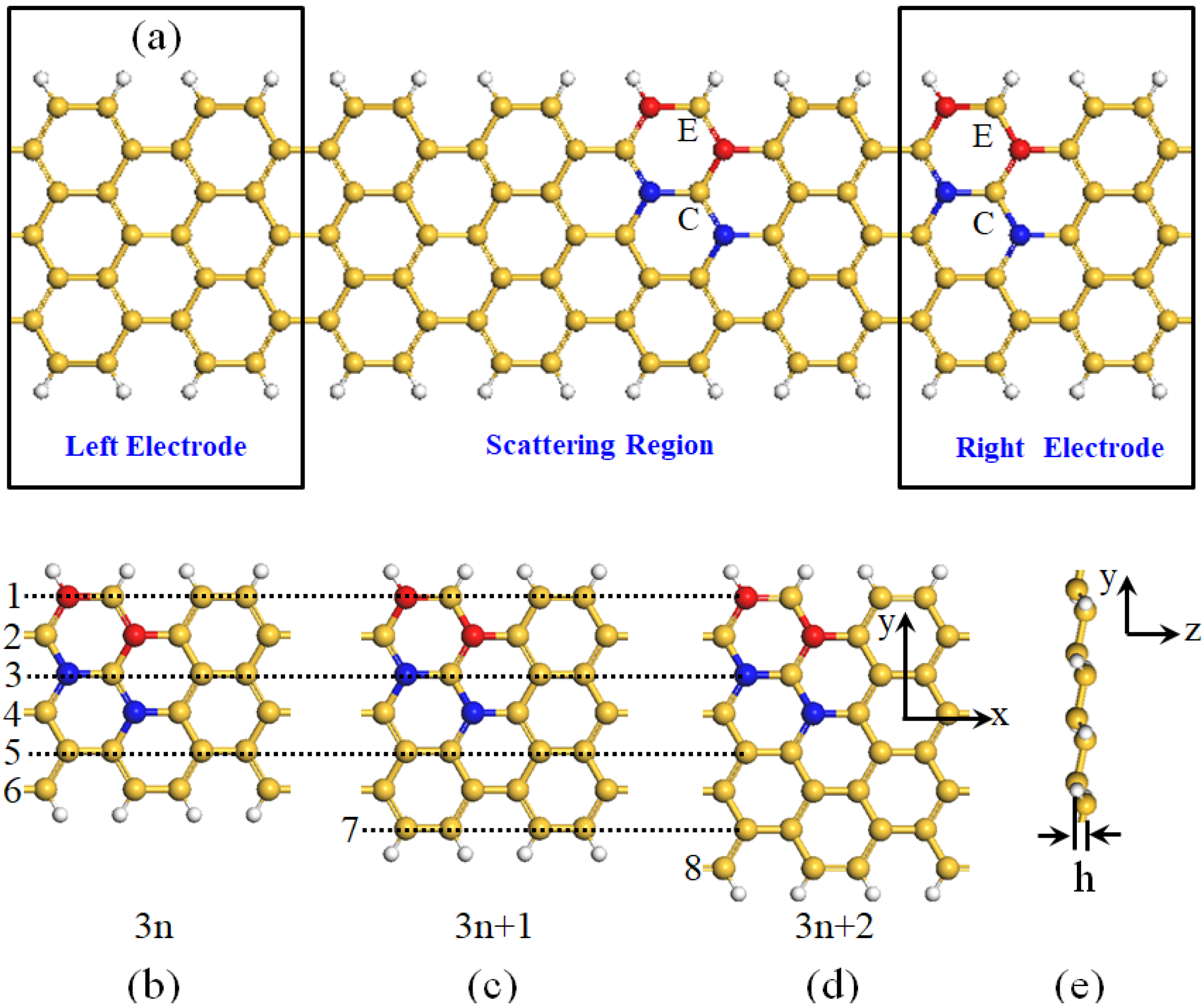
2 as an asymmetric electrode was constructed, as shown in
Figure 1a. It was composed of three parts, including a left electrode, a center scattering area, and a right electrode. The electrode was composed of two repeated silicon cells and the central scattering region was composed of four repeated silicon cells. It is well-known that SiNRs are similar to graphene nanoribbons (GNRs) in that their intrinsic properties depend on the width (W) of the nanoribbon; these were divided into three categories according to the width of the nanoribbon (W = 3n, 3n + 1, and 3n + 2, where n was an integer). Therefore, we selected ASiNRs with three widths—N = 6, 7, and 8, respectively—and these were named A6, A7, and A8. In addition, the center (edge) of the right electrode was diagonally embedded into the P atom pair and the constructed two-probe model was defined as A6/7/8-C/E (indicating ASiNRs with widths of 6, 7, and 8 as center-doped or edge-doped with AA-P
2, as shown in
Figure 1b–d.
Using a first-principles calculation based on density functional theory, the geometry and electronic band structure of the system were optimized by the SIESTA software package [
37]. The form of Perdew, Burke, and Ernzerhof uses the generalized gradient approximation (GGA) to represent the exchange correlation potential and the basic set of atomic orbitals uses the double ξ polarization (DZP) function [
38,
39]. The maximum cut-off kinetic energy was set to 200 Ry. For the N-ASiNRs system, we considered periodic boundary conditions in the x-direction of the coordinates and the distance between the two cells in the Z-direction was greater than 10 Å to ensure the isolated monolayer structure of the system. The Brillouin zone (BZ) was sampled using 15
1
1 Monkhorst–Pack k-points in the self-consistent total energy calculations. The TRANSIESTA-C software package was used to calculate the transport performance of the tow probes [
40]. The voltage transmission spectrum was calculated according to the standard equation:
where G is the Green’s function of the contact region, Γ
L/R is the coupling matrix, and V is the applied voltage bias. The computational formula for a current could be used; namely, the Landauer–Büttiker formula:
where
and
are the electrochemical potentials for the two electrodes and
is the transmission coefficient at energy E and bias voltage V.
3. Results and Discussion
As the stable structure of AA-P
2-diagonally doped ASiNRs (AA-P
2∠ASiNRs) had been determined in previous studies [
31], we gave the band structure of ideal central-doped and edge-doped ASiNRs, as shown in
Figure 2a–c. The ideal ASiNRs with widths of 3n and 3n + 1 showed semiconductivity and the ASiNRs with a width of 3n + 2 showed typical metal properties. However, both central and edge doping produce two impurity bands near the Fermi level. It is well-known that the doping band affects the electron transfer near the Fermi level, so we constructed a double probe transport model with the doping system as the central scattering region. On this basis, we first explored the current voltage (I–V) characteristics of the AA-P
2-diagonally doped ASiNR device; the voltage range was selected as −1.0 V to 1.0 V with a step of 0.05 V, as shown in
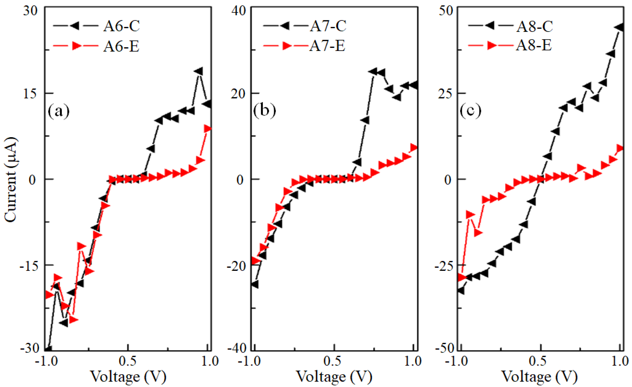
Figure 3a–c. It was evident that the I–V curves of almost all devices were asymmetric and exhibited typical semiconductor characteristics at corresponding threshold voltages. Compared with center doping, the edge doping system was more obvious. For example, when the voltage increased from 0 V to 0.6 V, the current of the A7-C system increased, but when the voltage was greater than 0.6 V, the current value of the system decreased instead; thus, a negative differential resistance effect appeared. The same was true for A6-C. According to the traditional definition of the rectification coefficient by R(V) = I(+V)/I(−V), the current values of the positive and negative voltages were in the same order of magnitude. When the current under a positive bias was much larger than the corresponding current under a negative bias, the rectification behavior was stronger. As can be seen from
Figure 4, within the range of 0.1 V–0.4 V, the rectification coefficient of A7-E decreased with the increase in the threshold voltage; it reached a maximum of 190 at 0.3 V, which was several times greater than the rectification ratio achieved by the molecular devices previously reported in the literature [
32,
41,
42] (
Table 1). In addition, compared with the doping of a single P atom reported by the research group of Zhang et al. [
43], the doping of AA-P
2 could generate more impurity energy bands, resulting in a more obvious negative differential effect and rectification behavior of rectifier devices under asymmetric electrodes. The research of nanodevices provides a theoretical basis. Other rectification coefficients vary in the range of 0–10. The rectification ratio of A7-C was smaller than that of A7-E and the variation range was not large; it was less than 20 at almost all threshold voltages. Meanwhile, the A8-E system achieved a maximum rectification ratio of 35 at a bias of 0.1 V. However, for the AA-P
2∠ASiNR device with a width of 6, the I–V curve was obviously different from that with a width of 7, showing a high symmetry. Therefore, a large proportion of rectification could only be obtained in the A7-E system; it was completely negligible in the other AA-P
2∠ASiNR systems.
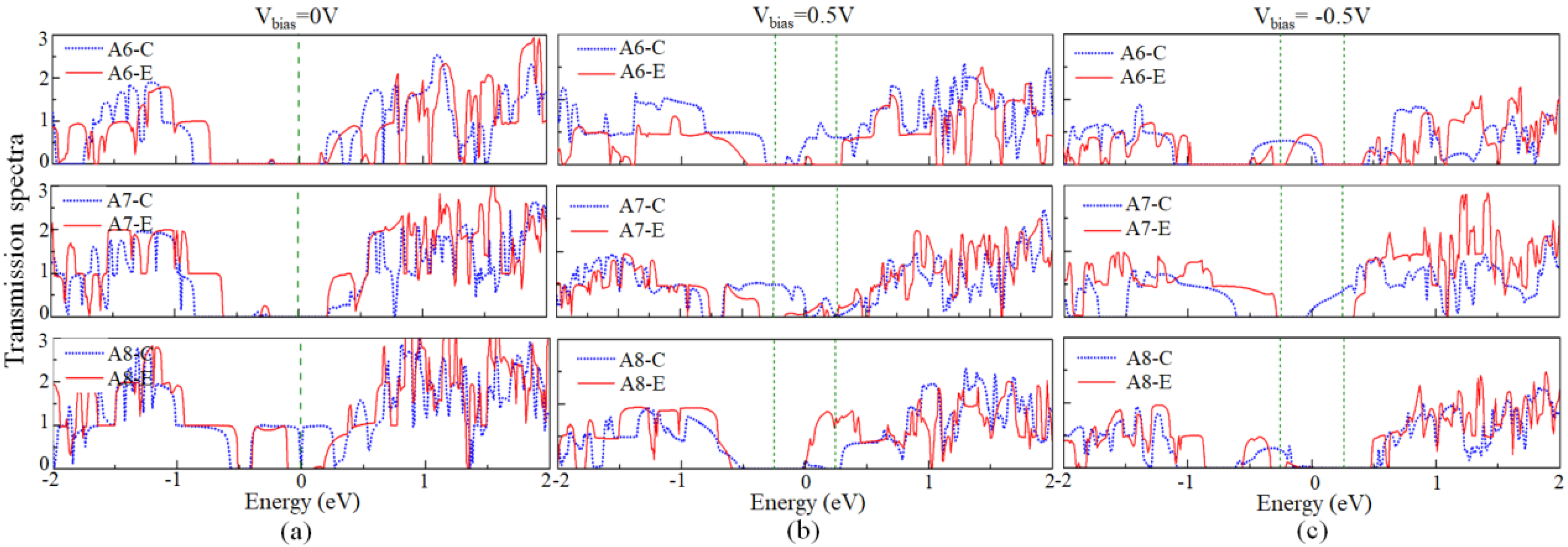
In order to understand the strong rectification effect, we calculated the transmission coefficient spectra of AA-P
2∠ASiNRs with widths of 6, 7, and 8 at 0 V, 0.5 V, and −0.5 V biases, respectively, as shown in
Figure 5. It is well-known that the transmission coefficient spectrum and the integral area in the bias window determine the magnitude of the current. First, the three central- or edge-doped AA-P
2 devices with different widths exhibited different family behaviors at a zero bias. When an additional bias was applied, we observed a more interesting phenomenon: for the A7-E system, a strong and wide peak in the transmission spectrum appeared in the bias window of V = 0.5 V, resulting in a large current in the device. However, when the bias V = −0.5 V, almost no peak could be found in the displayed bias window, so the system had a strong rectification behavior. For the A7-C system, although the peak value of the transmission spectrum was obvious in the V = 0.5 V bias window, when the opposite bias V = −0.5 V was applied, the transmission peak value was almost unchanged. This indicated that the magnitude of current under a positive and negative bias of the A7-C device was similar and the rectification effect was not obvious. When we changed the width of AA-P
2∠ASiNR to 8, the bias window of the A8-C device appeared with several peaks at 0.5 V with a certain current. At the bias of −0.5 V, the transmission peak was very small, indicating that the rectification ratio of A8-C had a certain fluctuation. For the A8-E system, a sharp peak appeared near the Fermi level at the 0.5 V bias and the peak almost disappeared at the −0.5 V bias. Therefore, the device also exhibited weak rectification behavior. However, for the AA-P
2∠ASiNR device with a width of 6, a strong and wide transmission peak appeared at the positive and negative 0.5 V bias. Due to the strong metallic properties, rectification behavior did not occur in the A6 device. In short, the rectification effect of the edge-doped AA-P
2∠ASiNRs was more superior.
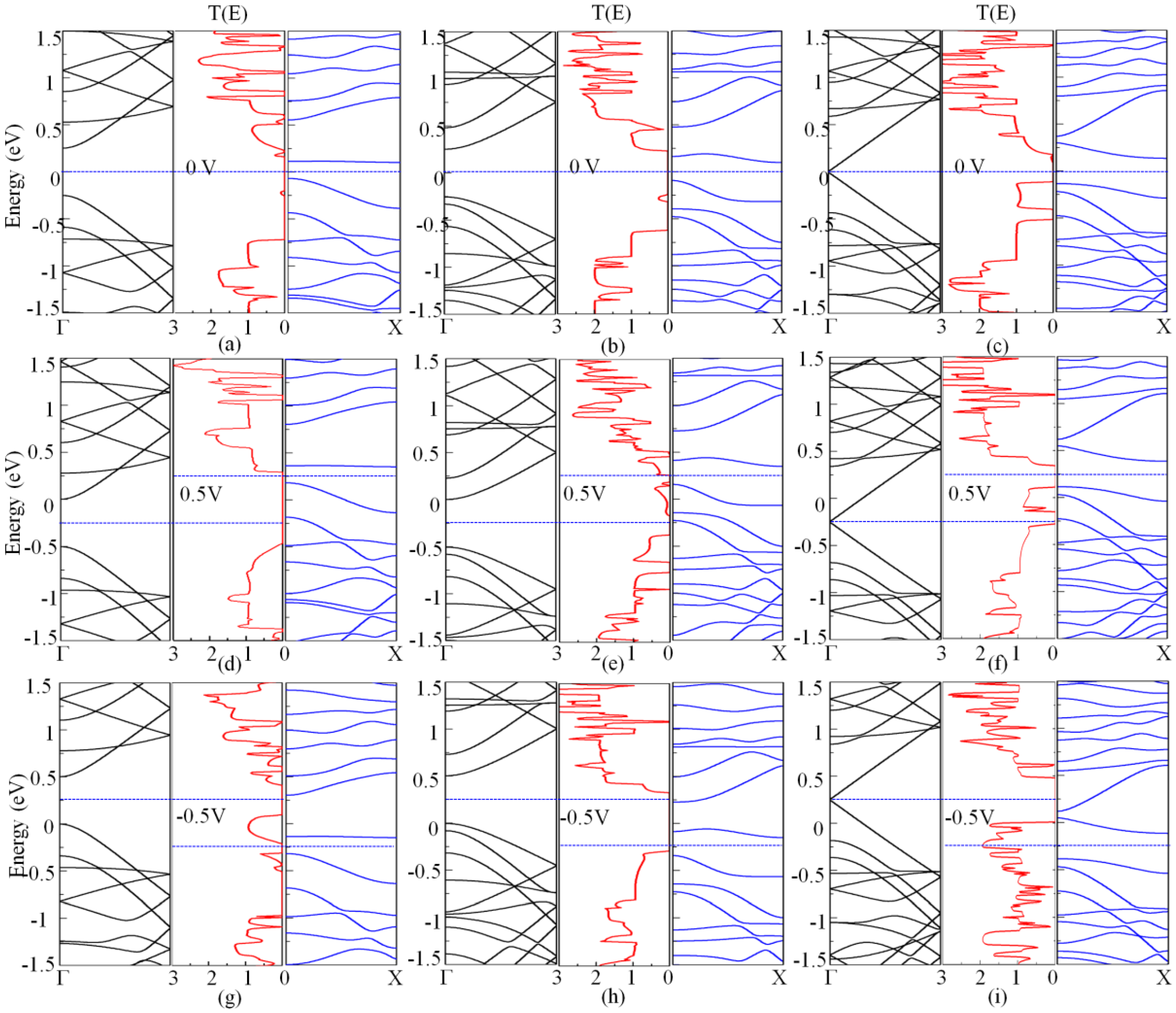
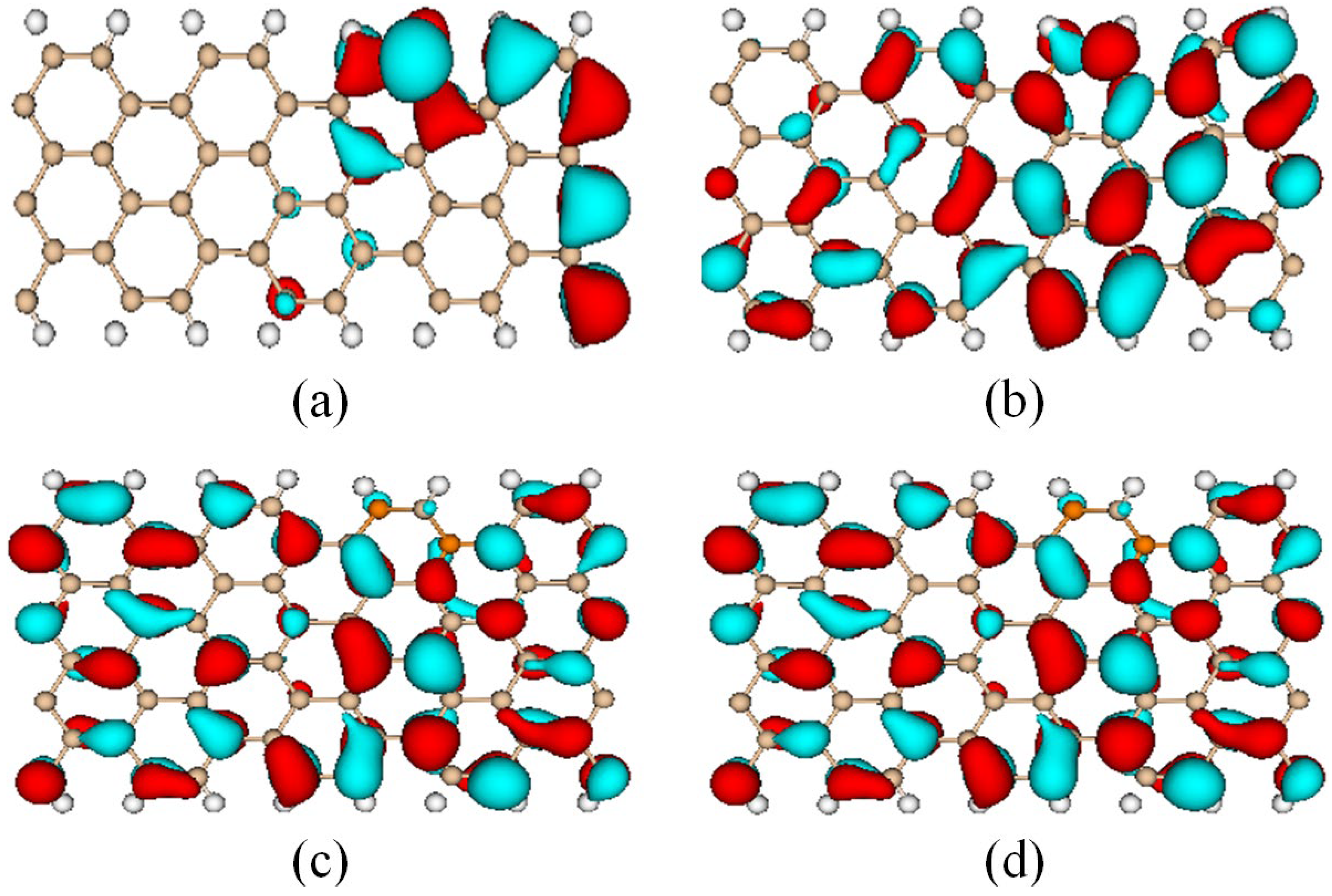
In order to clearly elucidate the rectification phenomenon of the AA-P
2∠ASiNR devices, the band structures of the left and right electrodes and corresponding transmission spectra of A6-E, A7-E, and A8-E at 0 V, 0.5 V, and −0.5 V, respectively, were further presented, as shown in
Figure 6. In this part, we only describe the edge-doped system (E) because almost all the central-doped system (C) exhibited metal characteristics and the rectification coefficient was relatively small compared with the E system. It is well-known that the magnitude of a current depends not only on the good matching of the band structures corresponding with the left and right electrodes, but also on the delocalization of the molecular projected self-consistent Hamiltonian (MPSH) energy state at the corresponding eigenvalue (E
v). Therefore, we also calculated the MPSH energy states of the A6-E, A7-E, and A8-E devices under certain E
vs, as shown in
Figure 7. As shown in
Figure 5, it was found that although the ideal ASiNRs where N = 6 and 7 exhibited semiconductor properties and the ideal ASiNRs where N = 8 exhibited gold properties, all the ASiNRs doped with AA-P
2 exhibited different band structures. The results showed that two new bands appeared near the Fermi level of the doped electrode (right electrode) and the impurity band changed with the width of the ASiNRs. It is well-known that each phosphorus atom can act as an electron donor and generate a new band around the Fermi energy according to the rules of electron arrangement outside the nucleus of phosphorus atoms, which is when impurity phosphorus atoms were introduced into the ideal ASiNRs. By doping the P atom pair, a delocalized state of the system was generated in the conduction band (CB) rather than in the valence band (VB). Thus, the extra electrons introduced by the impurity atom pair caused the valence band of the right electrode to move all the way down compared with the pristine ASiNRs. When a positive voltage was applied to the device, the energy band of the left electrode moved down and the energy band of the right electrode moved up compared with the Fermi level. With the movement of the energy bands of the left and right electrodes, the VB of the left electrode contacted the CB of the right electrode, forming an electronic channel, and then the transmission spectrum appeared in the transmission spectrum.
Due to the semiconductor characteristics of the ideal and AA-P
2-doped ASiNRs with a width of 6, an energy gap of about 0.52 eV appeared in the A6-E device near the Fermi level at the zero bias, as shown in
Figure 6a. When a bias of 0.5 V was applied to A6-E, the transmission peak did not appear in the bias window, which depended on the fact that the VB of the left electrode near the Fermi level did not match the CB of the right electrode. However, when the same negative bias was applied, the band of the left electrode shifted up and the band of the right electrode shifted down and a transmission peak could be observed near the Fermi level, depending on the maximum VB of the left electrode matching the impurity band of the right electrode, as shown in
Figure 6c. At the same time, the MPSH electron state at a −0.5V bias of the A6-E system at E
v = −0.21 eV was completely localized on the right side and the localization on the left side of the scattering region disappeared, which showed that there was a weak coupling between the scattering area and the ideal ASiNRs of the left electrode and signified that the transmission channel in the A6-E system under the −0.5V bias was suppressed, as shown in
Figure 7a. It could be seen that there were few states available for electron movement through the A6-E device, making the transmission coefficient relatively small; thus, a large proportion of rectification behavior could not be obtained.
As shown in
Figure 6b, the impurity bands in the A7 system with edge-doped AA-P
2 were distributed around the Fermi level and the energy gap was reduced compared with the pristine system. Under a zero bias, the upper part of the left electrode VB and the lower part of the right electrode CB had no matching energy band, so there was a relatively large gap between the valence band and the impurity band in the transmission spectrum, which was in the range of −0.25 eV–0.25 eV. When a positive bias was applied, a sharp peak appeared within the bias window, which varied greatly from the zero bias. At the same time, as shown in
Figure 7b, the MPSH of A7-E at E
v = 0.15 eV had a good delocalization state and formed an effective electron transport channel. However, when a negative bias was applied, the maximum VB of the left electrode did not match the impurity band of the right electrode in the bias window and there was no transmission peak. Therefore, the total amplitude of the transmission coefficient under a positive bias (0.5 V) was much larger than that under a negative bias (−0.5 V), resulting in a strong rectification effect.
For the A8-E device, the band mechanism of the perfect ASiNRs system exhibited typical metallic properties, the energy gap was opened by doping AA-P
2, and the band structure was changed, as shown in
Figure 6c. At a zero bias, the maximum value of the valence band of the left electrode did not match the minimum value of the conduction band of the right electrode in the energy range of −0.85 eV to 0.25 eV. Therefore, there was no transmission peak near the Fermi level. However, a strong transmission coefficient could clearly be seen in the rest of the energy range. When a 0.5 V bias was applied, the valence band part of the left electrode matched well with the conduction band of the right electrode due to the effect of the impurity band of the right electrode. As a result, a strong transmission coefficient appeared in the bias window. When a bias voltage of −0.5 V was applied, the conduction band of the left electrode partially matched the valence band of the right electrode; there was also a strong transmission coefficient within the bias window. The above results showed that the electron localization of MPSH at E
v = −0.07 eV under biases of 0.5 V and −0.5 V was good and the energy state distribution was very similar, as shown in
Figure 7c,d. Therefore, there was no obvious rectification behavior.
According to the above analysis, ASiNRs with a width W = 3n + 2 exhibited metallic properties whereas for W = 3n or 3n + 1, the system exhibited semiconductor properties and there was a certain energy gap near the Fermi level. When AA-P2 was doped into the semiconductor ASiNRs with widths of W = 3n or 3n + 1, the extra electron of the P atom was one more than that of the C atom; thus, these extra electrons filled the original empty conduction band and a corresponding doping band appeared near the Fermi level. Interestingly, the doping of AA-P2 still left an energy gap between the valence band and the conduction band of the ASiNR system. However, for metallic ASiNRs with the width W = 3n + 2, the energy gap opened near the Fermi level after the impurity band of AA-P2 doping, showing the semiconductor characteristics.
We now summarize the rectifying mechanism of the AA-P2-doped semiconductor ASiNR heterojunction. At a zero bias, although an impurity band appeared near the Fermi level on the AA-P2-doped right electrode due to the band gap on the left electrode, the transmittance remained zero. When a positive bias was applied, the band structure of the left electrode shifted upward whereas the band structure of the right electrode shifted downward. When the lowest conduction band of the left electrode and the highest conduction band of the right electrode were in contact with each other, electrons could be conducted from one electrode to the other, so an effective current could be observed. However, when a negative bias was applied, the band of the left electrode shifted downward whereas the right electrode shifted upward. Although the conduction band of the left electrode moved to the Fermi level, the energy band gap of the right electrode also moved to the Fermi level, so the electrons could not be conducted from the left electrode to the right electrode; thus, the transmission coefficient of the bias window was still zero and no current was formed. In this way, the rectifying behaviors of positive and negative voltages were more obvious.
Obviously, in the system exhibiting rectifying behaviors, there was a switching voltage during the current increase from zero, which depended on the energy gap of the left electrode. Therefore, as the width of the nanoribbon increased, the band gap correspondingly decreased, making the switching voltage in the I–V curve shift to the left. However, for systems with the widths 3n or 3n + 1, there was still a band gap near the Fermi level due to the effect of the impurity band after AA-P2 doping. In other words, all ASiNRs had a partially filled conduction band with a gap between the conduction band and the valence band, so a clear rectified behavior could be observed. As the width of the nanoribbon increased, the band gap of the electrode decreased, making the rectification region as a whole narrower and moving toward zero. In this way, it was deduced that when the bandwidth was wide enough, the rectification behavior would disappear.


