Article

Improved Performance of Perovskite Deep-Ultraviolet Photodetector Using FAPb(I/Br)3 as Light Absorption Layer

1
Department of Electrical Engineering, Gachon University, Seongnam 13120, Republic of Korea
2
Department of Intelligent Mechatronics Engineering, Sejong University, Seoul 05006, Republic of Korea
*
Authors to whom correspondence should be addressed.
Coatings 2023, 13(2), 341; https://doi.org/10.3390/coatings13020341
Submission received: 28 December 2022 / Revised: 12 January 2023 / Accepted: 30 January 2023 / Published: 2 February 2023
(This article belongs to the Special Issue Optical Thin Film and Photovoltaic (PV) Related Technologies)

Abstract

:
Constitutive engineering by adding halide anions is one effective way to improve the performance of photodetectors by adjusting the bandgap. In this study, a mixed-anion perovskite thin film was facile fabricated by post-processing of a pure FAPbI3 film with a formamidinium bromide (FABr) solution. In addition, the manufactured thin film was used as the light absorption layer, SnO2-SDBS as the electron transport layer, and spiro-OMeTAD as the hole injection layer to fabricate a deep ultraviolet(UV) photodetector. The device exhibited a response of 43.8 mA/W−1, a detectability of 3.56 × 10¹³ Jones, and an external quantum efficiency of 38%. Therefore, this study is promising for various applications in the deep-UV wavelength region.

1. Introduction

Ultraviolet (UV) photodetectors (PDs) convert UV energy into electrical signals and are devices that can detect weak UV energy due to their high detection rate [1,2]. These PDs have received considerable attention in the industry due to their diverse applications such as safety and precision control, and smoke and temperature sensing [3,4,5,6]. In the past, UV PDs were mainly manufactured using semiconductor materials such as ZnGa2O4, MoS2, MgZnO, or diamond. However, fabricating and manufacturing of UV PDs using these materials are complicated and expensive using epitaxy, RF magnetron sputtering, chemical vapor deposition, and the like, so it is an obstacle to commercialization [7,8,9,10]. Therefore, the development of inexpensive and simple UV PD is required.
In general, the wavelength range of ultraviolet rays is 100 to 400 nm, and it is classified into three areas of UVA (320 to 400 nm), UVB (280 to 320 nm), and UVC (100 to 280 nm) according to the effect on the biosphere. Ultraviolet rays have fatal effects on humans, such as skin aging, wrinkles, and skin cancer [11,12]. Earlier, UVC was mainly completely absorbed in the stratospheric ozone layer. It was generated only from artificial device sources such as sterilizers and arc xenon lamps for disinfecting air and water. Therefore, most PD research has been focused on UVA and UVB PD [13,14,15]. However, due to the destruction of the ozone layer by environmental pollution, UVC began to reach the earth’s surface [16]. Therefore, it is essential to study deep-UV PDs to detect light in the UVC range, which has high energy and destroys the genetic material in human cells and viruses, and has a more fatal effect on humans than UVA and UVB.
Organic-inorganic lead halide-based perovskite materials have excellent optoelectronic properties such as low photocurrent loss, bandgap tuning, high light absorption ability, and carrier mobility [17,18,19]. In addition, the fabrication of photonic devices using perovskite materials is relatively simple and economical [20]. Therefore, their use in the field of optical devices, such as solar cells and PDs, is continuously progressing [21,22]. A lot of structural engineering studies have been conducted to analyze the properties by adding br ions to Methylammonium lead iodide (MAPbI3), a commonly used perovskite material [23]. However, studies on the effect of br ions on the performance of formamidanium lead iodide (FAPbI3) are relatively lacking. FAPbI3 is more suitable for use in photodetectors because it has better light absorption in the deep ultraviolet region than MAPbI3 [24]. When the br ion is added, the lattice constant decreases, and the bond length of the atoms decreases because the Pb-br bond is shorter than the Pb-I bond. This reduction in bond length contributes to performance improvement in photodetector fabrication by improving light generation and carrier transport characteristics [25,26]. In addition, the addition of an appropriate amount of br ions improves the quality of the film due to the high bonding density of perovskite, helping to improve the optoelectronic performance of the device [27].
One of the important factors in deep-UV PD fabrication is the transmittance of the electron transport layer in the UVC (100 to 280 nm) region. Typically, titanium dioxide (TiO2) and [6,6]-phenyl C61 butyric acid methyl ester (PCBM) are used as electron transport layers in perovskite-based devices [28]. However, TiO2 and PCBM do not transmit light in the deep-UV wavelength range [29]. Therefore, TiO2 and PCBM are not suitable as electron transport layers for deep-UV PD. Therefore, using SnO2 as an electron transport layer having high transmittance in the deep ultraviolet wavelength region is essential for fabricating a deep-UV PD.
In this study, the aim was to fabricate a PD with higher characteristics in the deep-UV region than the existing pure FAPbI3-based PDs. It was achieved by injecting Br ions into formamidanium bromide (FABr) using a post-processing process. The performance of the fabricated deep-UV PD improved device characteristics such as external quantum efficiency (EQE), detectability, and responsiveness owing to the amelioration of thin film characteristics that result from electron mobility and crystal grain growth under the influence of injected Br. These results indicate that the mixed-anionic halide perovskite FAPb(I/Br)3 is a promising candidate for improving deep-ultraviolet PD performance.

2. Materials and Methods

2.1. Reagents and Materials

Pb(II) iodide (PbI2, 99.999%, Sigma Aldrich, St. Louis, MO, USA), 1-butyl alcohol (99%, Sigma Aldrich, St. Louis, MO, USA), sodium dodecylbenzenesulfonate (SDBS, Sigma Aldrich, St. Louis, MO, USA), acetonitrile (99.93%, Sigma Aldrich, St. Louis, MO, USA), ethyl alcohol (≥99.5%, Sigma Aldrich, St. Louis, MO, USA), dimethyl sulfoxide (DMSO, ≥99.9%, Sigma Aldrich, St. Louis, MO, USA), N,N-dimethylformamide (DMF, 99.8%, Sigma Aldrich, St. Louis, MO, USA), 2,2,7,7-tetrakis[N,N-di(4-methoxyphenyl)amino]-9,9-spirobifluorene (spiro-OMeTAD, 99%, Sigma Aldrich, St. Louis, MO, USA), 2-propanol (IPA; 75 wt%, Sigma Aldrich, St. Louis, MO, USA), bis(trifluoromethane)sulfonimide lithium salt (Li-TSFI; ≥99.0%, Sigma Aldrich, St. Louis, MO, USA), toluene (99.9%, Sigma Aldrich, St. Louis, MO, USA), and 4-tertbutylpyridine (98%, Sigma Aldrich, St. Louis, MO, USA). Formamidinium iodide (FAI, GreatCell SolarKorea, Seohyun, Republic of Korea), Formamidanium bromide (Fabr, GreatCell SolarKorea, Seohyun, Republic of Korea), and methylammonium hydrochloride(MACl, GreatCell SolarKorea, Seohyun, Republic of Korea). Indium tin oxide(ITO) is deposited on a quartz-glass substrate (TMA, Seoul, Republic of Korea). A SnO2 colloidal solution (15 wt% in water, Alfa Aesar, Haveril, MA, USA). All materials were used without further purification.

2.2. Fabrication of Mixed Anion Perovskite Photodetector Based on FAPb(I/Br)3

ITO-coated quartz substrates (8 Ω m/sq) were sequentially cleaned with neutral detergent, isopropanol, acetone, ethanol, and deionized water using an ultrasonic bath. Thereafter, the substrate was dried using a drying oven and treated with UV ozone for 10 min to complete the cleaning process. After diluting 2.4 mL of a SnO2 colloidal solution (15% by weight) with 9.2 mL of deionized water, 2 mg of SDBS was dissolved using the diluted SnO2 solution to prepare a SnO2-SDBS mixed solution. The SnO2-SDBS mixed solution was spin-coated at 3000 rpm for 25 s on the cleaned substrate and then annealed at 150 °C for 30 min to be used as the electron transport layer of the device. Substrates were then treated with UV ozone for 20 min before perovskite deposition. The perovskite FAPbI3 precursor solution was prepared by mixing PbI2 (1.4 mol) and FAI (1.0 mol) in a DMSO:DMF (10:1, v/v) solvent system. After stirring for 1 h, MACl was added to the prepared precursor solution and further stirred for 30 min. Immediately prior to coating, the solution was filtered through a 0.45-μm syringe filter. Solutions for FABr post-processing were stirred for 2 h with IPA and FABr (5, 10, 15, 20, and 25 mg). The precursor solution was deposited by spin coating at 4500 rpm for 25 s, and then an anti-solvent process was performed with toluene for the last 10 s. After that, the post-processing solution was spin-coated at 4500 rpm for 25 s and annealed for 20 min. After cooling at 25 °C for 10 min, a spiro-OMeTAD solution [1 mL chlorobenzene consisting of 72.3 mg spiro-OMeTAD, 28.8 μL 4-tert-butyl pyridine and 17.5 μL Li-TFSI solution (ACN in 1 mL of 520 mg Li-TSFI)] was deposited onto the perovskite film at 3000 rpm for 20 s. Finally, 85 nm Au was thermally evaporated through an electrode in a high vacuum (2 × 10⁶ Torr) using an e-beam evaporator. A schematic diagram of the fabrication method and device for perovskite thin films is shown in Figure 1a.

2.3. Characterization of the Fabricated PD and Device Measurement

X-ray diffraction (XRD, SmartLab, Rigaku, Tokyo, Japan) was performed using Cu Kα radiation (λ = 1.542 Å), and the device used gracing incidence geometry. A field emission scanning electron microscope (FE-SEM, Hitachi, S-4700, Tokyo, Japan) was used to analyze the surface and cross-sectional morphology of the perovskite layer. The absorption characteristics of the perovskite films were recorded using an ultraviolet-visible spectrophotometer (Agilent, 8453 UV-vis, Santa Clara, CA, USA). Electrical signals from the photodetector were recorded using a Sourcemeter (Keithley, 2400, Cleveland, OH, USA). A 254-nm UV lamp (Vilber, VL6.LC, Seine-et-Marne, France) was used as the light source for UV irradiation. The mobility, resistivity, and carrier concentration of the films were recorded using a Hall effect measurement system (Ecopia, HMS-3000, Anyang, Republic of Korea).

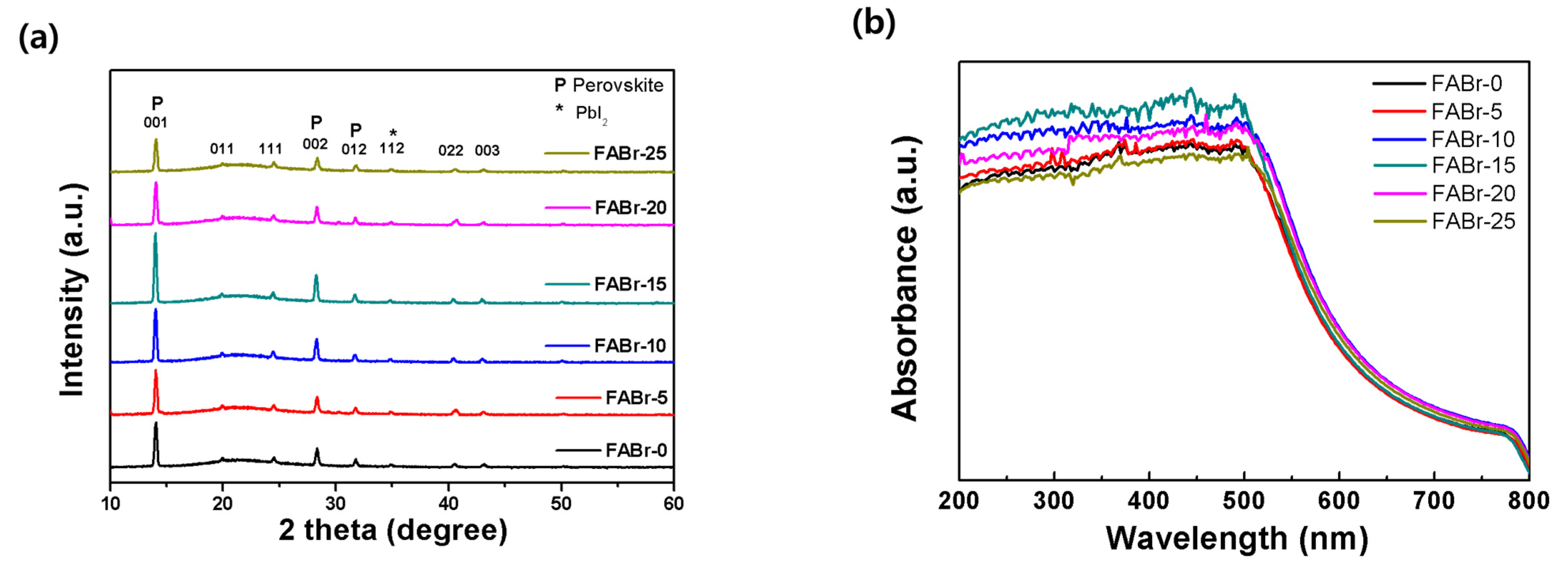
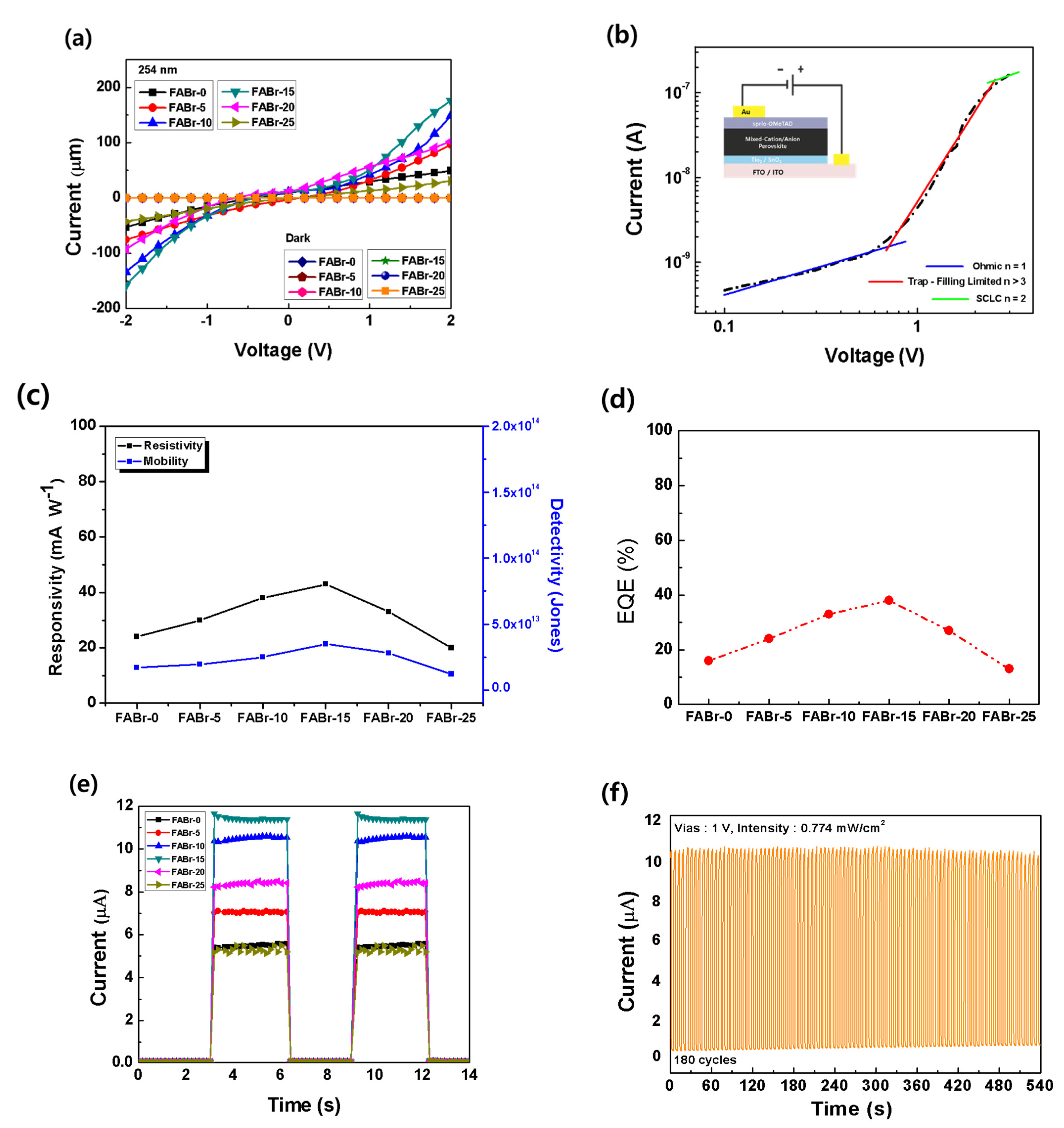
3. Results and Discussion

Characteristics of the Prepared Mixed-Anion Perovskite Film

Fabricated perovskite thin films are defined as FABr-0, FABr-5, FABr-10, FABr-15, FABr-20, and FABr-25 according to the concentration of FABr. To analyze the morphology and microstructure of the perovskite film, the surface morphology of the perovskite film post-treated with FABr observed by SEM is shown (Figure 2). The perovskite crystals on the surface of FABr-0 showed non-uniform growth and small particle size. As the amount of FABr gradually increased, the particle size of the perovskite thin film increased and the surface of the thin film was densely improved, resulting in changes in the microstructure. Average particle sizes for FABr-0, FABr-5, FABr-10, FABr-15, FABr-20 and FABr-25 were measured to be ~150 nm, ~270 nm, ~410 nm, ~580 nm, ~560 nm and ~550 nm, respectively. FABr-15 showed the most uniform grain growth and surface morphology without pinholes. These results indicate improved photoelectric properties such as higher extinction coefficients and longer carrier lifetimes [30,31]. When the concentration of FABr was further increased, the number of pinholes increased and non-uniform grain growth was observed. This is due to the dewetting phenomenon caused by the high concentration of FA+ [32,33]. This dewetting phenomenon shrinks crystal grains and creates gaps between crystal grains, affecting the crystallinity of perovskite and adversely affecting the performance of optical devices [34,35]. As a result, these morphological surface changes, uniformity, and grain growth mean that intermediate engineering using the optimal amount of FABr addition greatly affects the microstructure of the perovskite active layer [36].
To investigate the effect of FABr post-processing on the final crystal formation of the mixed anion perovskite film, XRD patterns of the crystalline properties of the film are shown (Figure 3a). First, it shows that the main peak of perovskite around 14° increases with the Br concentration. The crystallinity of the FABr-15 film has been improved to show the highest peak intensity, and the post-processing film using FABr-15 has a 2.5-fold increase in peak intensity compared to FABr-0. The decrease in peak intensity above the concentration of FABr in FABr-15 demonstrates that excessive FA+ causes grain shrinkage, which adversely affects the crystallinity during the crystallization of the film. Also, show that excessive doping of Br in FAPbI3 reduces the stability of the perovskite phase [26]. This significant improvement in film crystallinity after FABr treatment is fully consistent with the structural evolution of previously studied results [37].
The UV-vis absorption spectra in Figure 3b were used to characterize the photophysical properties of mixed anion perovskite films prepared by post-processing with different concentrations of FABr. The results show a relative improvement in the absorption spectra, with films post-treated with FABr exhibiting stronger absorption than FABr-0 films. The extinction coefficient increased as the concentration of FABr increased and was strongest in FABr-15. This is because the grains grew after the FABr treatment, increasing the extinction coefficient [38]. It also indicates that the addition of an appropriate amount of br ions increased the bonding density and thus improved the quality of the film, which affected the absorbance [27].
Optoelectronic properties such as carrier concentration, resistivity, and mobility of thin films are important parameters for semiconductor materials and power devices [38]. Therefore, the photoelectric properties of the thin film according to the FABr concentration were analyzed using a Hall effect measurement system. All prepared films had high carrier concentration values of greater than 3.0 × 1013 cm−3. The mobility of the film that was not treated with FABr was 17.59 cm2/V∙s and FABr-15 had the highest mobility of 38.21 cm2/V∙s. This increase in mobility is related to the Pb-X (where X = I and Br) structure of perovskite. The bond length of atoms decreases as the Br concentration increases. This is due to the smaller ionic radius of Br atoms. Also, the electron charge distribution is much stronger around the Br atom due to its higher electronegativity value (2.96) compared to I (2.66) [25,26]. In conclusion, heavy Pb atoms interact strongly with Br atoms due to their high electronegativity difference, resulting in a decrease in bond length, and increasing mobility. The decrease in mobilities of the FABr-20 and FABr-25 films is because excessive amounts of FABr adversely affect the perovskite crystal formation. The photogenerated current varies with mobility, and high mobility produces high photocurrent [39,40]. The diffusion coefficient is calculated using the Einstein relation D = μKBT/q. (Boltzmann constant KB = 1.3806488 × 10⁻²³ J/K, absolute temperature T of the sample, charge q) Since the diffusion coefficient is proportional to the diffusion distance, high mobility has a significant effect on the diffusion distance [41]. Thus, the addition of a moderate amount of FABr reduces the trap density due to the increase in diffusion distance. Table 1 details the photoelectric properties of the films.
The performance of the PD according to the FABr concentration was analyzed by studying the current-voltage (I-V) curve from −2 to +2 V at a scan rate of 0.1 V with a 254 nm-light source with an output of 0.774 mW/cm2 under dark conditions. A Schottky barrier is formed in the fabricated PD due to contact between the electrodes and the current flow.
Figure 4a–f shows the amount of photoprogression produced by this device. FABr-0, which was not post-treated with FABr, produced photocurrents of 52 and 50 µA at −2 and +2 V, respectively. However, FABr-15 post-treated with FABr produced the highest photocurrents of 158 µA at −2 V and 175 µA at +2 V. This shows that the post-processing of FABr increased the photocurrent generation by approximately three times.
The performance of the photodetector according to the change in FABr concentration is shown in Figure 5a. In Figure 5b, the I−V characteristics change rapidly as the voltage bias increases. This I−V characteristic trend curve is consistent with the space-charge-limiting current where the trapped charge exists [42]. At a low bias, the I−V characteristic trend follows an ohmic response. This proves that an ohmic contact is formed at the interface of the fabricated deep-UV PD. After entering a high bias space charge limited current (SCLC) region, the current is approximately proportional to V2+n, where n is the improvement factor due to trap filling. In addition, a saturation of the photocurrent occurs due to the Schottky contact formed between the electrodes [43].
Figure 5c shows the responsivity (R) and the specific detectability (D*) of the device. R is a parameter representing the efficient response of a PD to a light signal and is defined as R = I p h   o r   V p h P [ A W 1   o r   V W 1 ] where Photocurrent (Iph) = ILightIDark, output Photovoltage (Vph) = VLightVDark, and P∈ is the incident power, and the output photovoltage or photocurrent is divided by the input photo power of the active area of the PD. The R values of the fabricated device for FABr-0, FABr-5, FABr-10, FABr-15, FABr-20, and FABr-are 24.1, 30.5, 38.7 43.8, 33.2, and 20.8 mA W−1, respectively.
Furthermore, D* is one of the important performance parameters that allows the evaluation of performance changes caused by the changes in the material and structure used when manufacturing a PD and represents the minimum level of light output that a PD can detect. D* is primarily affected by the responsiveness and noise of the PD. The three noises that contribute are the dark current, Johnson’s shot noise, and thermal fluctuation “flicker” noise [44]. The shot noise of the double dark current is assumed to have the greatest effect and is defined as D * = R 2 q J D a r k [ J o n e s ] where q is the charge and Jdark is the dark current density. Further, because R and D* values are directly proportional, the higher the R-value, the higher the D* value. The D* values of the fabricated device for FABr-0, FABr-5, FABr-10, FABr-15, FABr-20, and FABr-25 are 1.71 × 10¹³, 1.95 × 10¹³, 2.51 × 10¹³, 3.56 × 10¹³, 2.84 × 10¹³, and 1.24 × 10¹³ Jones, respectively.
EQE, which represents the conversion efficiency of the PD and is calculated as the ratio of the number of collected charge carriers to the number of incident photons, is another parameter that represents the performance of the fabricated PD. EQE = R h c e λ where h is Planck’s constant, c is the speed of light, and λ is the wavelength of the incident light. The EQE values of the device for FABr-0, FABr-5, FABr-10, FABr-15, FABr-20, and FABr-25 are 16, 24, 33, 38, 27, and 13%, respectively.
Figure 5e shows the current-time (I−T) response characteristics of a far-UV PD measured at a bias voltage of 1 V and an output luminous intensity of 0.774 mW/cm2. Response speed and response time are inversely proportional to each other and are parameters that evaluate the performance of PDs. When the signal input to the PD changes over time, a time delay occurs until the output of the device is reached, which is the response time. The response speed indicates the rapid duration at which a PD responds to an optical signal and is expressed in terms of the rise time and fall time. In general, the rise time is defined as the time required for the response to increasing from 10 to 90% of its maximum value, whereas fall time is defined as the opposite. The rise time (trise) and fall time (tfall) of the fabricated device for FABr-0, FABr-5, FABr-10, FABr-15, FABr-20, and FABr-25 were 66 ms/68 ms, 72 ms/75 ms, 78 ms/79 ms, 78 ms/79 ms, 74 ms/76 ms, and 65 ms/67 ms, respectively.
Figure 5f shows the operational on/off characteristics of deep-UV PD with film post-processing using FABr-15 as the light-absorbing layer. Testing of the device with more than 180 on/off cycles showed stable reproducibility. The photocurrents were 11.12 μA in the first iteration and 10.98 μA after 180 iterations. These results demonstrate the excellent reproducibility of the fabricated PD.
The performance parameters for mixed-anion perovskite deep-UV PDs fabricated with FABr-15 were similar or superior to those of PDs reported in previous studies (Table 2).

4. Conclusions

In summary, a mixed-anion perovskite PD fabricated through a post-processing process was fabricated. The fabricated device showed excellent photoelectric properties for a deep ultraviolet light source of 254 nm. In addition, the detectability of 3.56 × 10¹³ Jones showed better characteristics than other perovskite-based PDs. Therefore, this study demonstrated a PD with a high detection rate that can operate under the deep-UV region.

Author Contributions

Sample fabrication and original draft preparation, S.B.H.; experimental supporting and editing, S.K.; supervision and editing, H.W.C. All authors have read and agreed to the published version of the manuscript.

Funding

This research was supported by the Basic Science Research Capacity Enhancement Project through the Korea Basic Science Institute (National Research Facilities and Equipment Center) grant funded by the Ministry of Education (2019R1A6C1010016) and the Korea Institute for Advancement of Technology (KIAT) grant funded by the Korean Government (MOTIE) (P0012451, The Competency Development Program for Industry Specialist).

Institutional Review Board Statement

Not applicable.

Informed Consent Statement

Not applicable.

Data Availability Statement

Not applicable.

Conflicts of Interest

The authors declare no conflict of interest.

References

  1. Razeghi, M.; Rogalski, A. Semiconductor ultraviolet detectors. J. Appl. Phys. 1996, 79, 7433–7473. [Google Scholar] [CrossRef]
  2. Li, C.; Ma, Y.; Xiao, Y.; Shen, L.; Ding, L. Advances in perovskite photodetectors. InfoMat 2020, 2, 1247–1256. [Google Scholar] [CrossRef]
  3. Hatzinikolaou, D.G.; Lagesson, V.; Stavridou, A.J.; Pouli, A.E.; Lagesson-Andrasko, L.; Stavrides, J.C. Analy-sis of the gas phase of cigarette smoke by gas chromatography coupled with UV-diode array detection. Anal. Chem. 2006, 78, 4509–4516. [Google Scholar] [CrossRef]
  4. Zheng, W.; Lin, R.; Zhang, Z.; Huang, F. Vacuum-ultraviolet photodetection in few-layered h-BN. ACS Appl. Mater. Interfaces 2018, 10, 27116–27123. [Google Scholar] [CrossRef]
  5. Gökkavas, M.; Butun, S.; Caban, P.; Strupinski, W.; Ozbay, E. Integrated AlGaN quadruple-band ultraviolet photodetectors. Semicond. Sci. Technol. 2012, 27, 065004. [Google Scholar] [CrossRef]
  6. Ulmer, M.P. A review of UV detectors for astrophysics: Past, present, and future. Quantum Sens. Nanophotonic Devices VI 2009, 7222, 317–328. [Google Scholar] [CrossRef]
  7. Zhang, X.L.; Hui, K.S.; Hui, K.N. High photo-responsivity ZnO UV detectors fabricated by RF reactive sput-tering. Mater. Res. Bull. 2013, 48, 305–309. [Google Scholar] [CrossRef]
  8. Gautam, C.; Verma, A.; Chaudhary, P.; Yadav, B.C. Development of 2D based ZnO–MoS2 nanocomposite for photodetector with light-induced current study. Opt. Mater. 2022, 123, 111860. [Google Scholar] [CrossRef]
  9. Liu, Z.; Li, F.; Li, S.; Hu, C.; Wang, W.; Wang, F.; Lin, F.; Wang, H. Fabrication of UV photodetector on TiO2/diamond film. Sci. Rep. 2015, 5, 14420. [Google Scholar] [CrossRef]
  10. Shewale, P.S.; Yu, Y.S. UV photodetection properties of pulsed laser deposited Cu-doped ZnO thin film. Ceram. Int. 2017, 43, 4175–4182. [Google Scholar] [CrossRef]
  11. Webb, R.B. Lethal and mutagenic effects of near-ultraviolet radiation. In Photochemical and Photobiological Reviews; Springer: Boston, MA, USA, 2015. [Google Scholar] [CrossRef]
  12. Maher, V.M.; Ouellette, L.M.; Curren, R.D.; McCormick, J.J. Frequency of ultraviolet light-induced mutations is higher in xeroderma pigmentosum variant cells than in normal human cells. Nature 1976, 261, 593–595. [Google Scholar] [CrossRef]
  13. Parrish, J. UV-A: Biological Effects of Ultraviolet Radiation with Emphasis on Human Responses to Longwave Ultraviolet; Springer Science & Business Media: Berlin, Germany, 2022. [Google Scholar]
  14. Omnès, F.; Monroy, E.; Muñoz, E.; Reverchon, J.L. Wide Bandgap UV Photodetectors: A Short Review of Devices and Applications; Gallium Nitride Materials and Devices II: San Jose, CA, USA, 2007; pp. 111–125. [Google Scholar]
  15. Jun, J.H.; Seong, H.; Cho, K.; Moon, B.M.; Kim, S. Ultraviolet photodetectors based on ZnO nanoparticles. Ceram. Int. 2009, 35, 2797–2801. [Google Scholar] [CrossRef]
  16. Tienaho, J.; Silvan, N.; Muilu-Mäkelä, R.; Kilpeläinen, P.; Poikulainen, E.; Sarjala, T. Ultraviolet absorbance of Sphagnum magellanicum, S. fallax and S. fuscum extracts with seasonal and species-specific variation. Photochem. Photobiol. Sci. 2021, 20, 379–389. [Google Scholar] [CrossRef]
  17. Miyata, A.; Mitioglu, A.; Plochocka, P.; Portugall, O.; Wang, J.T.W.; Stranks, S.D.; Snaith, H.J.; Nicholas, R.J. Direct measurement of the exciton binding energy and effective masses for charge carriers in organic–inorganic tri-halide perovskites. Nat. Phys. 2015, 11, 582–587. [Google Scholar] [CrossRef]
  18. Ning, W.; Wang, F.; Wu, B.; Lu, J.; Yan, Z.; Liu, X.; Sum, T.C.; Gao, F. Long electron–hole diffusion length in high-quality lead-free double perovskite films. Adv. Mater. 2018, 30, 1706246. [Google Scholar] [CrossRef]
  19. Ng, C.H.; Lim, H.N.; Hayase, S.; Zainal, Z.; Huang, N.M. Photovoltaic performances of mono-and mixed-halide structures for perovskite solar cell: A review. Renew. Sustain. Energy Rev. 2018, 90, 248–274. [Google Scholar] [CrossRef]
  20. Tong, G.; Li, H.; Zhu, Z.; Zhang, Y.; Yu, L.; Xu, J.; Jiang, Y. Enhancing hybrid perovskite detectability in the deep ultraviolet region with down-conversion dual-phase (CsPbBr3–Cs4PbBr6) films. J. Phys. Chem. Lett. 2018, 9, 1592–1599. [Google Scholar] [CrossRef]
  21. Park, N.G. Perovskite solar cells: An emerging photovoltaic technology. Mater. Today 2015, 18, 65–72. [Google Scholar] [CrossRef]
  22. Pan, S.; Li, J.; Wen, Z.; Lu, R.; Zhang, Q.; Jin, H.; Chen, Y.; Wang, S. Halide perovskite materials for photo (electro) chemical applications: Dimensionality, heterojunction, and performance. Adv. Energy Mater. 2022, 12, 2004002. [Google Scholar] [CrossRef]
  23. Jacobsson, T.J.; Correa-Baena, J.P.; Pazoki, M.; Saliba, M.; Schenk, K.; Grätzel, M.; Hagfeldt, A. Exploration of the compositional space for mixed lead halogen perovskites for high efficiency solar cells. Energy Environ. Sci. 2016, 9, 1706–1724. [Google Scholar] [CrossRef]
  24. Yuan, D.X.; Gorka, A.; Xu, M.F.; Wang, Z.K.; Liao, L.S. Inverted planar NH 2 CH [double bond, length as m-dash] NH 2 PbI 3 perovskite solar cells with 13.56% efficiency via low temperature processing. Phys. Chem. Chem. Phys. 2015, 17, 19745–19750. [Google Scholar] [CrossRef]
  25. Rehman, W.; Milot, R.L.; Eperon, G.E.; Wehrenfennig, C.; Boland, J.L.; Snaith, H.J.; Johnston, M.B.; Herz, L.M. Charge-carrier dynamics and mobilities in formamidinium lead mixed-halide perovskites. Adv. Mater. 2015, 27, 7938–7944. [Google Scholar] [CrossRef] [PubMed]
  26. Slimi, B.; Mollar, M.; Ben Assaker, I.; Kriaa, A.; Chtourou, R.; Marí, B. Synthesis and characterization of perovskite FAPbBr3−x Ix thin films for solar cells. Mon. Für Chem.-Chem. Mon. 2017, 148, 835–844. [Google Scholar] [CrossRef]
  27. Ni, X.; Lei, L.; Yu, Y.; Xie, J.; Li, M.; Yang, S.; Wang, M.; Liu, J.; Zhang, H.; Ye, B. Effect of Br content on phase stability and performance of H2N= CHNH2Pb (I1 − xBrx) 3 perovskite thin films. Nanotechnology 2019, 30, 165402. [Google Scholar] [CrossRef]
  28. Yang, Y.; Peng, H.; Liu, C.; Arain, Z.; Ding, Y.; Ma, S.; Liu, X.; Hayat, T.; Alsaedi, A.; Dai, S. Bi-functional additive engineering for high-performance perovskite solar cells with reduced trap density. J. Mater. Chem. A. 2019, 7, 6450–6458. [Google Scholar] [CrossRef]
  29. Lu, G.; He, F.; Pang, S.; Yang, H.; Chen, D.; Chang, J.; Lin, Z.; Zhang, J.; Zhang, C. A PCBM-modified TiO2 blocking layer towards efficient perovskite solar cells. Int. J. Photoenergy 2017, 2017, 1–9. [Google Scholar] [CrossRef]
  30. Liu, B.; Wang, S.; Ma, Z.; Ma, J.; Ma, R.; Wang, C. High-performance perovskite solar cells with large grain-size obtained by the synergy of urea and dimethyl sulfoxide. Appl. Surf. Sci. 2019, 467, 708–714. [Google Scholar] [CrossRef]
  31. Guo, X.; Yu, W.; Li, J.; Jiang, Z.; Ma, D.; Liu, H. Improving microstructure and photoelectric performance of the perovskite material via mixed solvents. Int. J. Inorg. Mater. 2017, 32, 870–876. [Google Scholar]
  32. Wu, P.; He, J.; Zhang, F. Vacuum thermal evaporation saved MA-free perovskite. Joule 2022, 6, 1394–1396. [Google Scholar] [CrossRef]
  33. Slimi, B.; Mollar, M.; Assaker, I.B.; Kriaa, I.; Chtourou, R.; Marí, B. Perovskite FA1-xMAxPbI3 for solar cells: Films formation and properties. Energy Procedia 2016, 102, 87–95. [Google Scholar] [CrossRef]
  34. Bai, S.; Cheng, N.; Yu, Z.; Liu, P.; Wang, C.; Zhao, X.Z. Cubic: Column composite structure (NH2CH= NH2) x (CH3NH3) 1-xPbI3 for efficient hole-transport material-free and insulation layer free perovskite solar cells with high stability. Electrochim. Acta 2016, 190, 775–779. [Google Scholar] [CrossRef]
  35. Mateen, M.; Arain, Z.; Liu, C.; Yang, Y.; Liu, X.; Ding, Y.; Hayat, T.; Alsaedi, A. High-Quality (FA)x (MA)1 − x PbI3 for Efficient Perovskite Solar Cells via a Facile Cation-Intermixing Technique. ACS Sustain. Chem. Eng. 2019, 7, 11760–11768. [Google Scholar] [CrossRef]
  36. Yang, Z.; Chueh, C.C.; Liang, P.W.; Crump, M.; Lin, F.; Zhu, Z.; Jen, A.K.Y. Effects of formamidinium and bromide ion substitution in methylammonium lead triiodide toward high-performance perovskite solar cells. Nano Energy 2016, 22, 328–337. [Google Scholar] [CrossRef]
  37. Chen, B.X.; Li, W.G.; Rao, H.S.; Xu, Y.F.; Kuang, D.B.; Su, C.Y. Large-grained perovskite films via FAxMA1 – x Pb (IxBr1 − x) 3 single crystal precursor for efficient solar cells. Nano Energy 2017, 34, 264–270. [Google Scholar] [CrossRef]
  38. Koizumi, S.; Umezawa, H.; Pernot, J.; Suzuki, M. Power Electronics Device Applications of Diamond Semiconductors; Woodhead Publishing: Sawston, UK, 2018; pp. 99–189. [Google Scholar]
  39. Zou, Y.; Zhang, Y.; Hu, Y.; Gu, H. Ultraviolet detectors based on wide bandgap semiconductor nanowire: A review. Sensors 2018, 18, 2072. [Google Scholar] [CrossRef]
  40. Myronov, M. Molecular Beam Epitaxy of High Mobility Silicon, Silicon Germanium and Germanium Quantum Well Heterostructures. In Molecular Beam Epitaxy; Elsevier: Amsterdam, The Netherlands, 2018; pp. 37–54. [Google Scholar]
  41. Cai, J.; Chen, X.; Hong, R.; Yang, W.; Wu, Z. High-performance 4H-SiC-based pin ultraviolet photodiode and investigation of its capacitance characteristics. Opt. Commun. 2014, 333, 182–186. [Google Scholar] [CrossRef]
  42. Marinov, O.; Deen, M.J.; Datars, R. Compact modeling of charge carrier mobility in organic thin-film transistors. J. Appl. Phys. 2009, 106, 06450. [Google Scholar] [CrossRef]
  43. Li, G.; Gao, R.; Han, Y.; Zhai, A.; Liu, Y.; Tian, Y.; Wu, Y.; Cui, Y. High detectivity photodetectors based on perovskite nanowires with suppressed surface defects. Photonics Res. 2020, 8, 1862–1874. [Google Scholar] [CrossRef]
  44. Gong, X.; Tong, M.; Xia, Y.; Cai, W.; Moon, J.S.; Cao, Y.; Nilsson, B.; Heeger, A.J. High-detectivity polymer photodetectors with spectral response from 300 nm to 1450 nm. Science 2009, 325, 1665–1667. [Google Scholar] [CrossRef]
  45. Shin, S.G.; Bark, C.W.; Choi, H.W. Study on Performance Improvements in Perovskite-Based Ultraviolet Sensors Prepared Using Toluene Antisolvent and CH3NH3Cl. Nanomaterials 2021, 11, 1000. [Google Scholar] [CrossRef] [PubMed]
  46. Zhang, Z.; Zheng, W.; Lin, R.; Huang, F. High-sensitive and fast response to 255 nm deep-UV light of CH3NH3PbX3 (X = Cl, Br, I) bulk crystals. R. Soc. Open Sci. 2018, 5, 180905. [Google Scholar] [CrossRef] [PubMed]
  47. Nguyen, T.M.H.; Kim, S.; Bark, C.W. Solution-processed and self-powered photodetector in vertical architecture using mixed-halide perovskite for highly sensitive UVC detection. J. Mater. Chem. A 2021, 9, 1269–1276. [Google Scholar] [CrossRef]
  48. Shao, D.; Zhu, W.; Liu, X.; Li, M.; Chen, J.; Sun, Y.Y.; Lian, J.; Sawyer, S. Ultrasensitive UV photodetector based on interfacial charge-controlled inorganic perovskite–polymer hybrid structure. ACS Appl. Mater. Interfaces 2020, 12, 43106–43114. [Google Scholar] [CrossRef] [PubMed]
Figure 1. (a) Manufacturing process of mixed anionic perovskite FAPb(I/Br)3; (b) Schematic diagram of Deep-UV PD.
Coatings 13 00341 g001
Figure 2. SEM images of mixed-anion perovskite according to FABr concentration (a) FABr-0, (b) FABr-5, (c) FABr-10, (d) FABr-15, (e) FABr-20, (f) FABr-25, (g) Cross-section of a device with individual layers shown in different colors.
Coatings 13 00341 g002aCoatings 13 00341 g002b
Figure 3. Characteristics of films of mixed-anionic perovskites according to FABr concentration. (a) XRD pattern, (b) UV-vis absorption spectrum in the deep-UV region, (c) photoelectric characteristics.
Coatings 13 00341 g003aCoatings 13 00341 g003b
Figure 4. Current-voltage (I−V) characteristics of mixed-anion perovskite PDs as a function of FABr concentration. (a) FABr-0, (b) FABr-5, (c) FABr-10, (d) FABr-15, (e) FABr-20, (f) FABr-25.
Coatings 13 00341 g004
Figure 5. Characteristics of the PD measured under 254 nm illumination with a power of 0.774 mW/cm2. (a) Current-voltage (I−V) characteristics of Deep-UV PD according to FABr concentration, (b) Double logarithmic I−V curve of Deep-UV PD with the highest photosensitivity under dark conditions, (c) Calculated R as a function of voltage and D*, (d) EQE, (e) Time−current (I−t) curves as a function of FABr concentration, (f) Transient photoresponse of prepared Deep-UV PDs during 180 ON/OFF switching cycles.
Coatings 13 00341 g005
Table 1. Comparison of resistivity, mobility, and carrier concentration of thin films according to the amount of FABr addition.
SampleResistivity
(Ω∙cm)
Mobility
(cm2/V∙s)
Carrier Concentration
(cm−3)
FABr-00.383217.593.506 × 1013
FABr-50.296225.544.065 × 1013
FABr-100.272327.125.353 × 1013
FABr-150.329738.215.430 × 1013
FABr-200.356717.374.248 × 1013
FABr-250.463510.173.8245 × 1013
Table 2. Comparison of important parameters of various perovskite-based deep-UV PDs.
MaterialsLight
(nm)
MethodVoltage
(V)
Responsivity
(mA/W)
Detectivity
(Jones)
EQE
(%)
Ref.
FAPb(I/Br)3254Solution243.83.56 × 101338[this study]
MAPbBr3254Solution-14.571.02 × 101322.2[45]
MAPbCl3255Single crystals5450-219[46]
MAPbBr3255Single crystals5300-146[46]
MAPbI3255Single crystals5120-58[46]
CsPbBr3-Cs4PbBr6254Vapor049.401.2 × 101231[20]
(FAPbI3)0.97(MAPbBr3)0.03254Solution052.684.65 × 101128[47]
CsCu2I3265pulsed laser237.78.1 × 101017.9[48]
Disclaimer/Publisher’s Note: The statements, opinions and data contained in all publications are solely those of the individual author(s) and contributor(s) and not of MDPI and/or the editor(s). MDPI and/or the editor(s) disclaim responsibility for any injury to people or property resulting from any ideas, methods, instructions or products referred to in the content.

