
Thin-Film Coating Methods: A Successful Marriage of High-Quality and Cost-Effectiveness—A Brief Exploration


Abstract
:1. Introduction
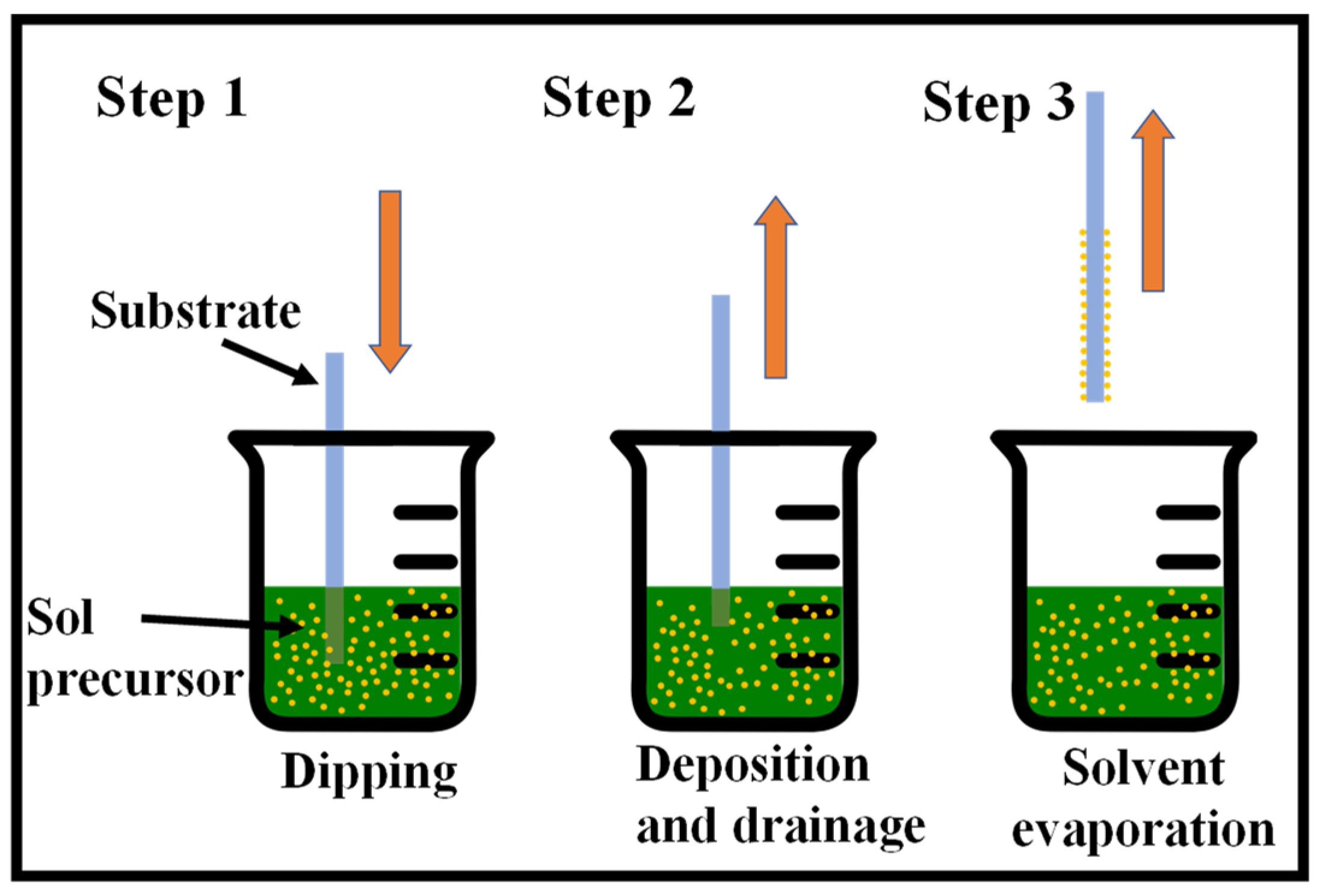
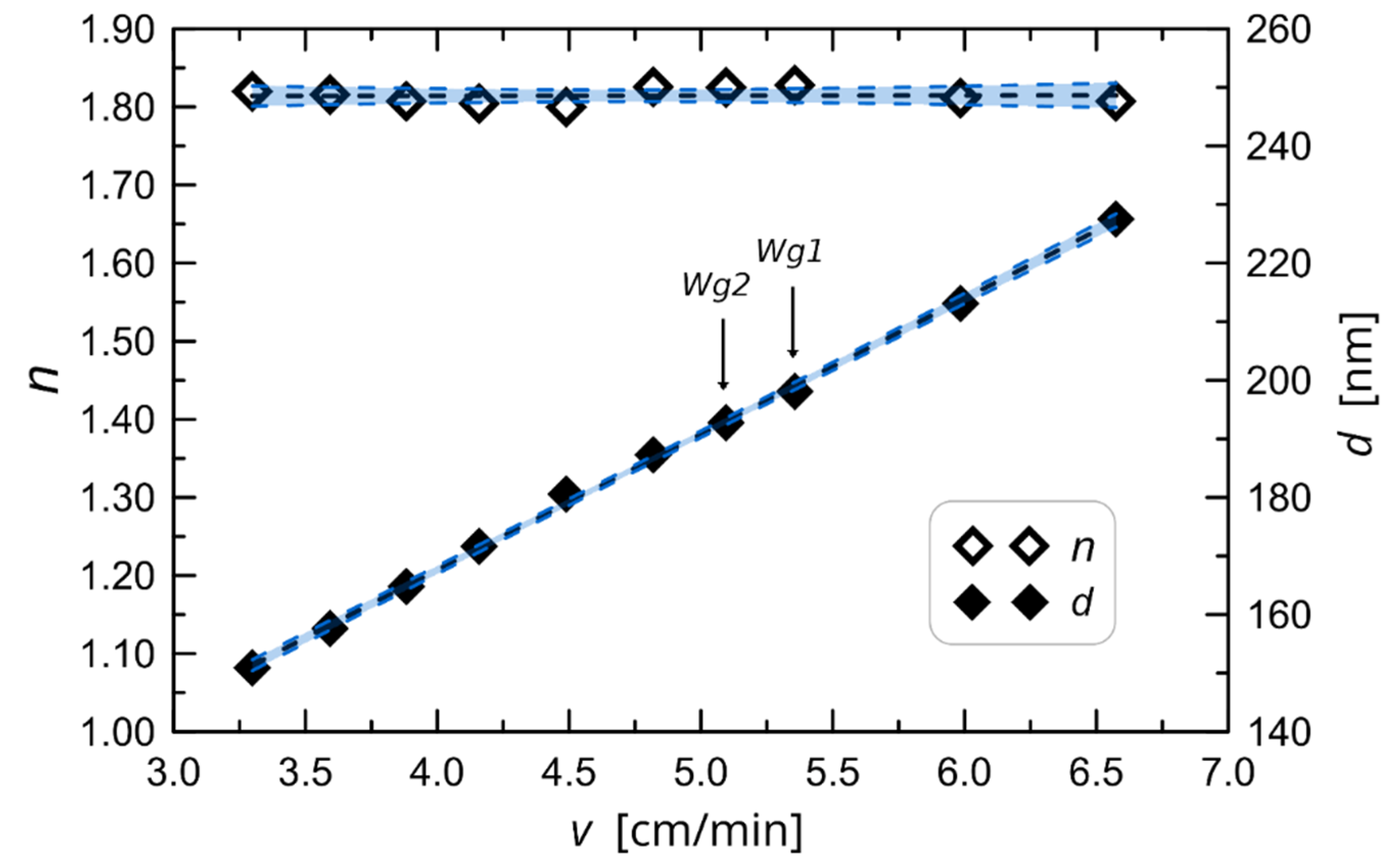
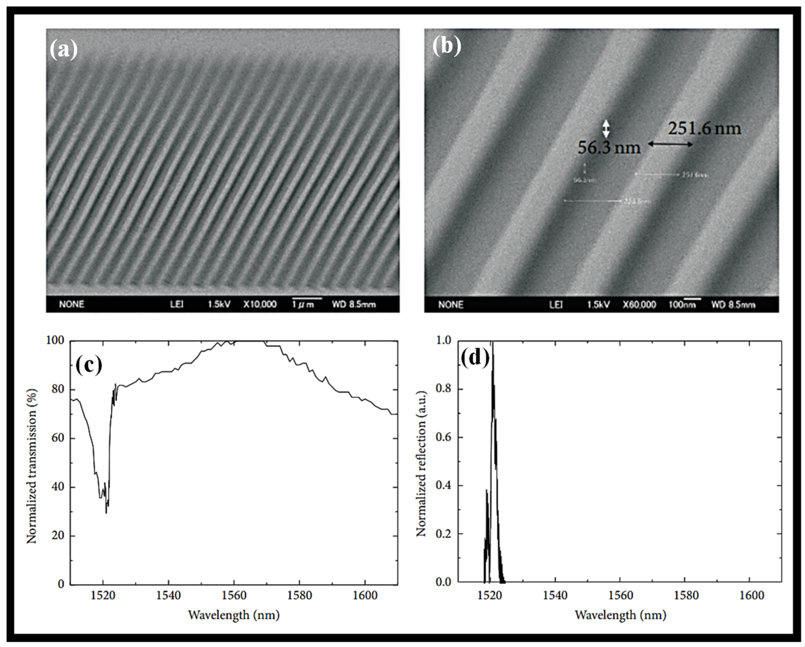
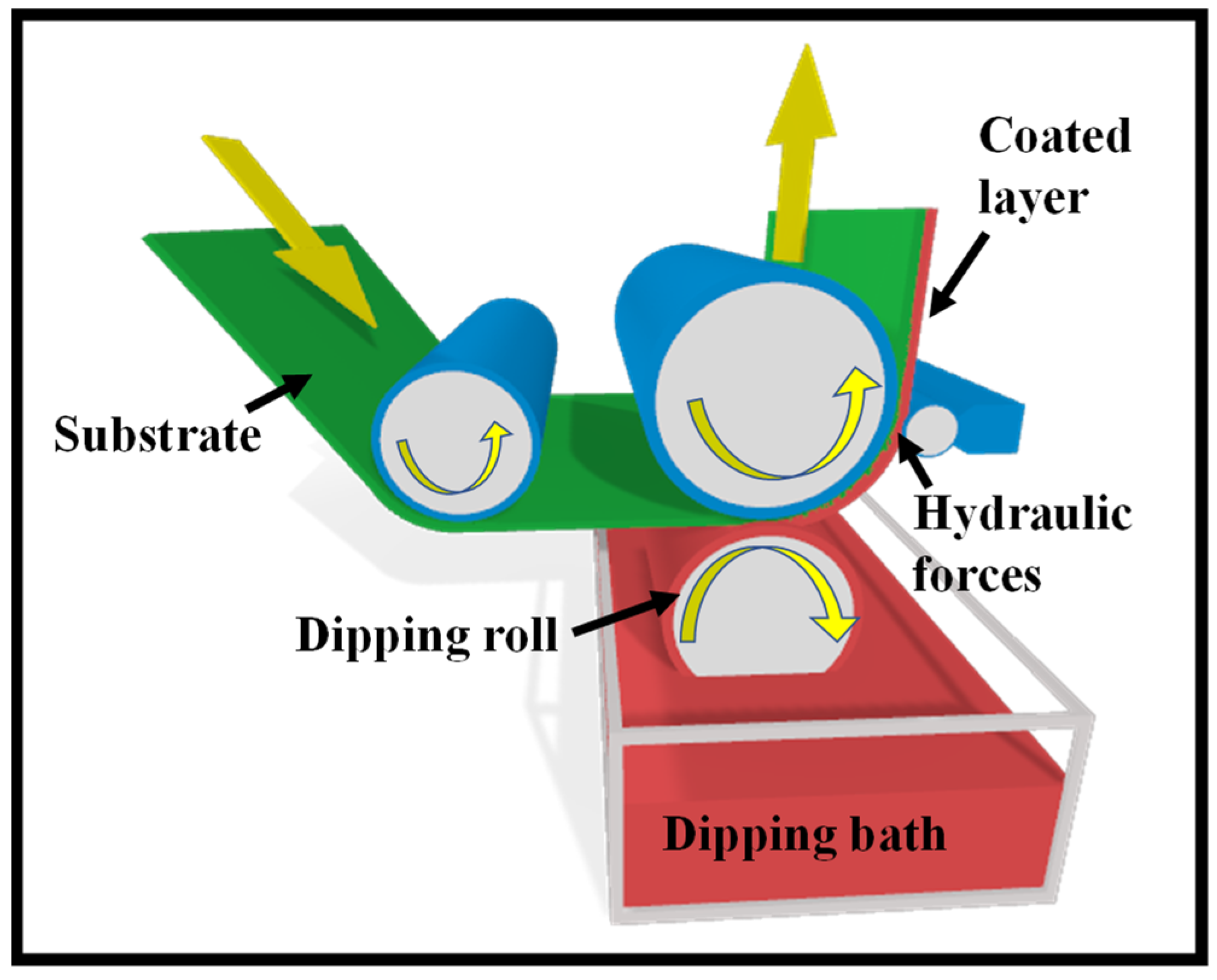
2. Dip-Coating
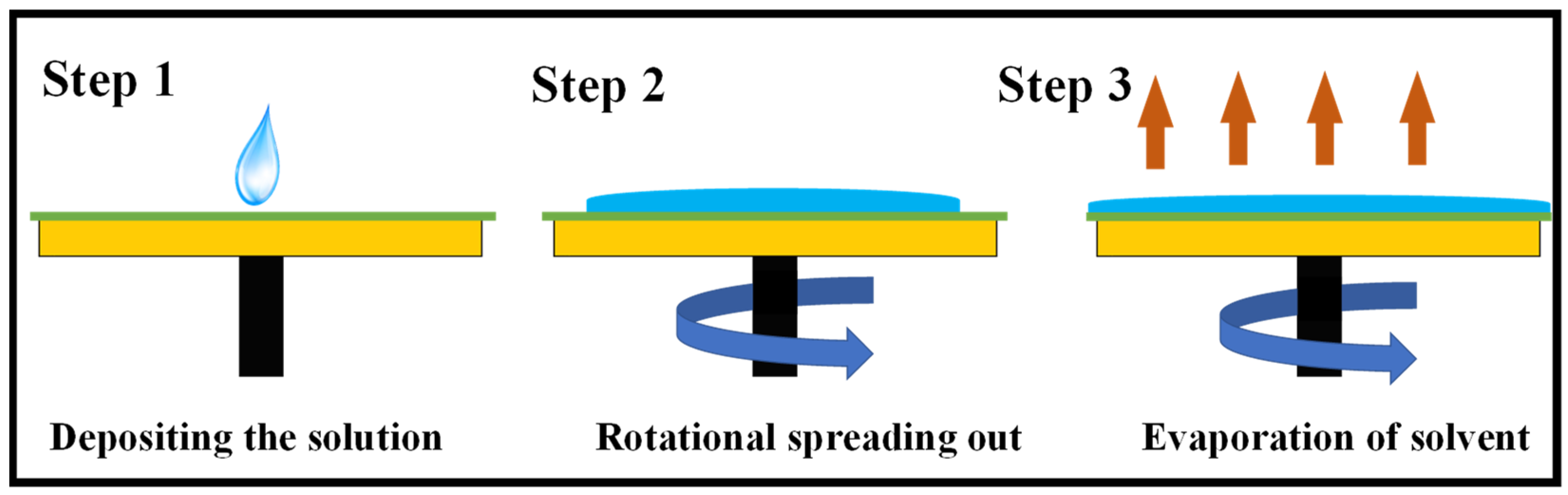
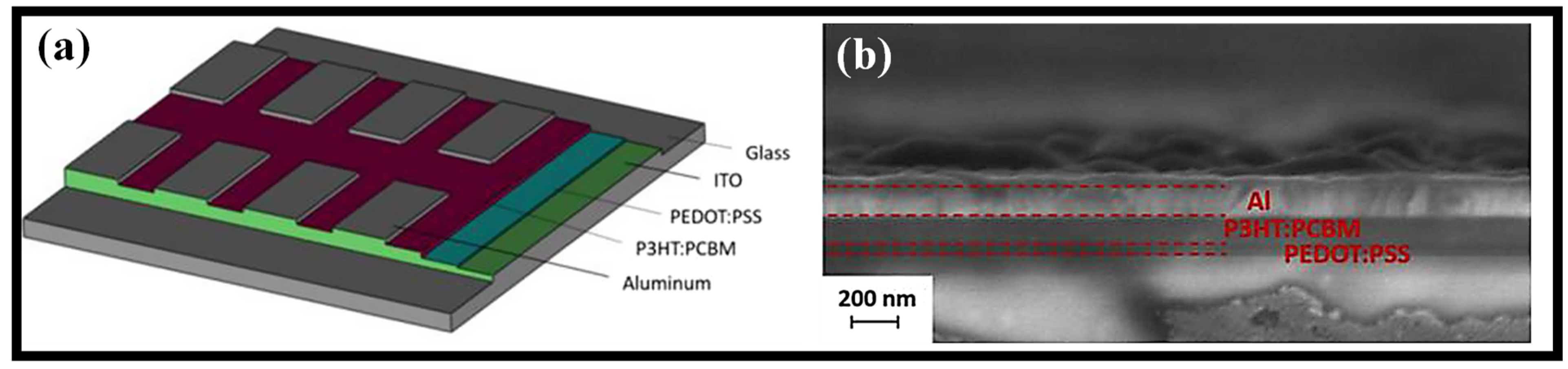
3. Spin-Coating
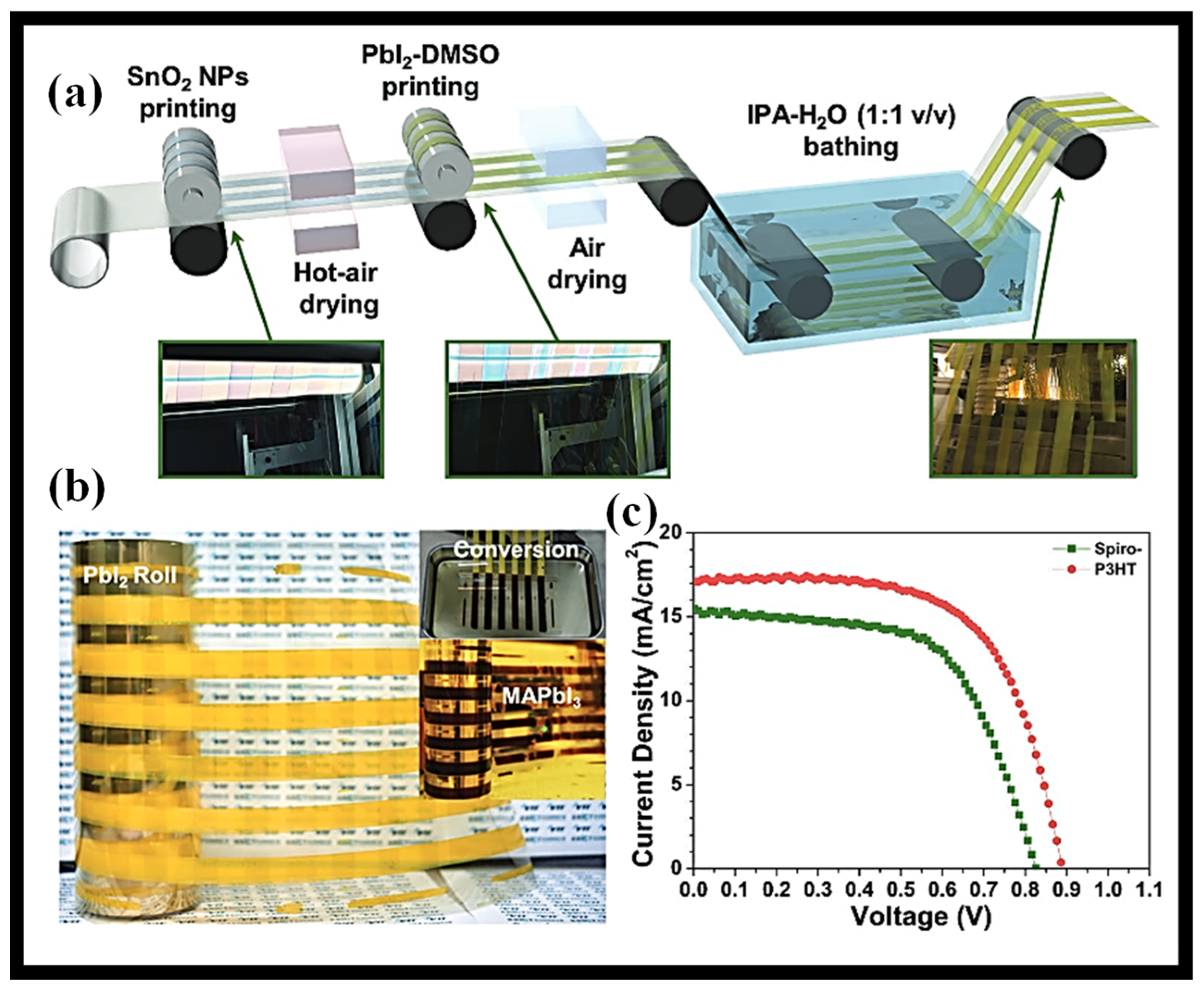
4. Roll-Coating
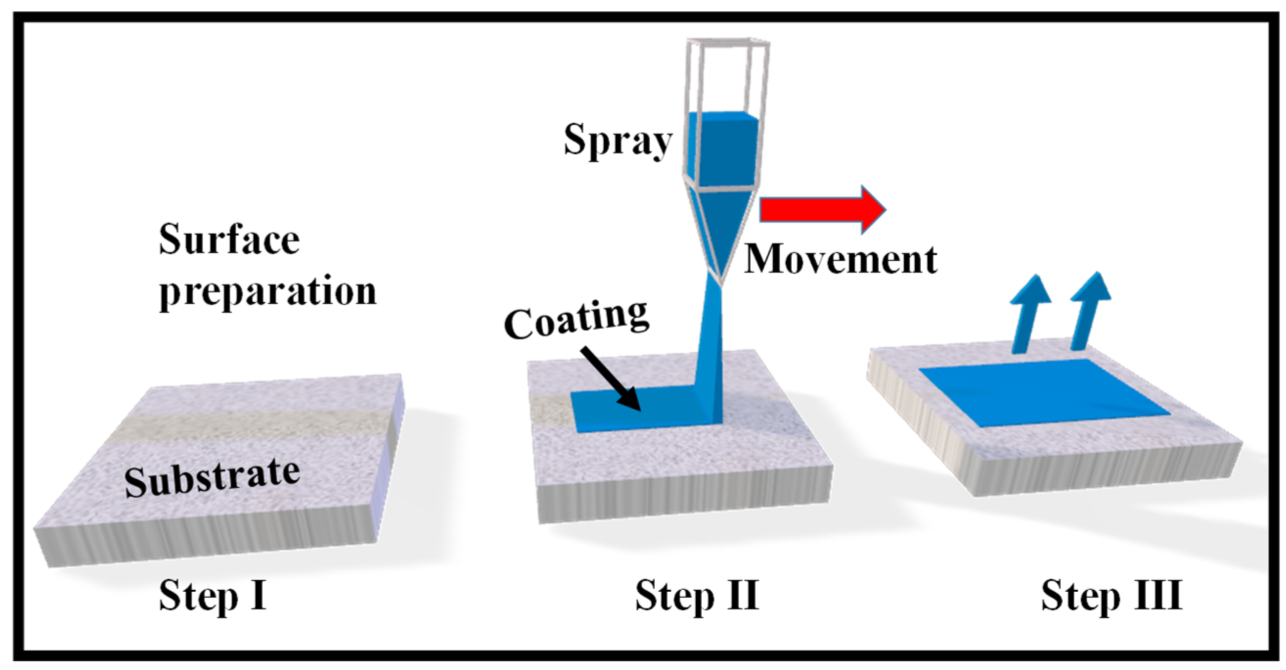
5. Spray-Coating
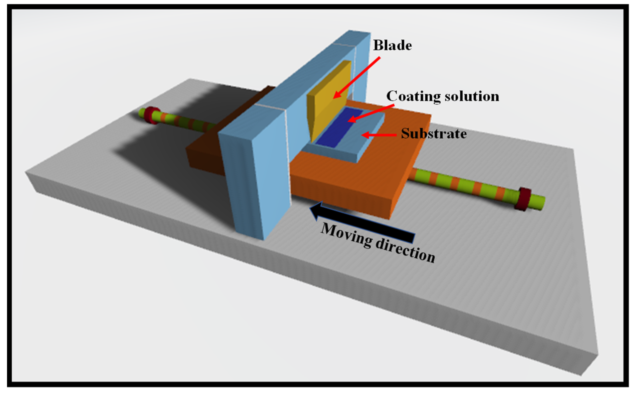
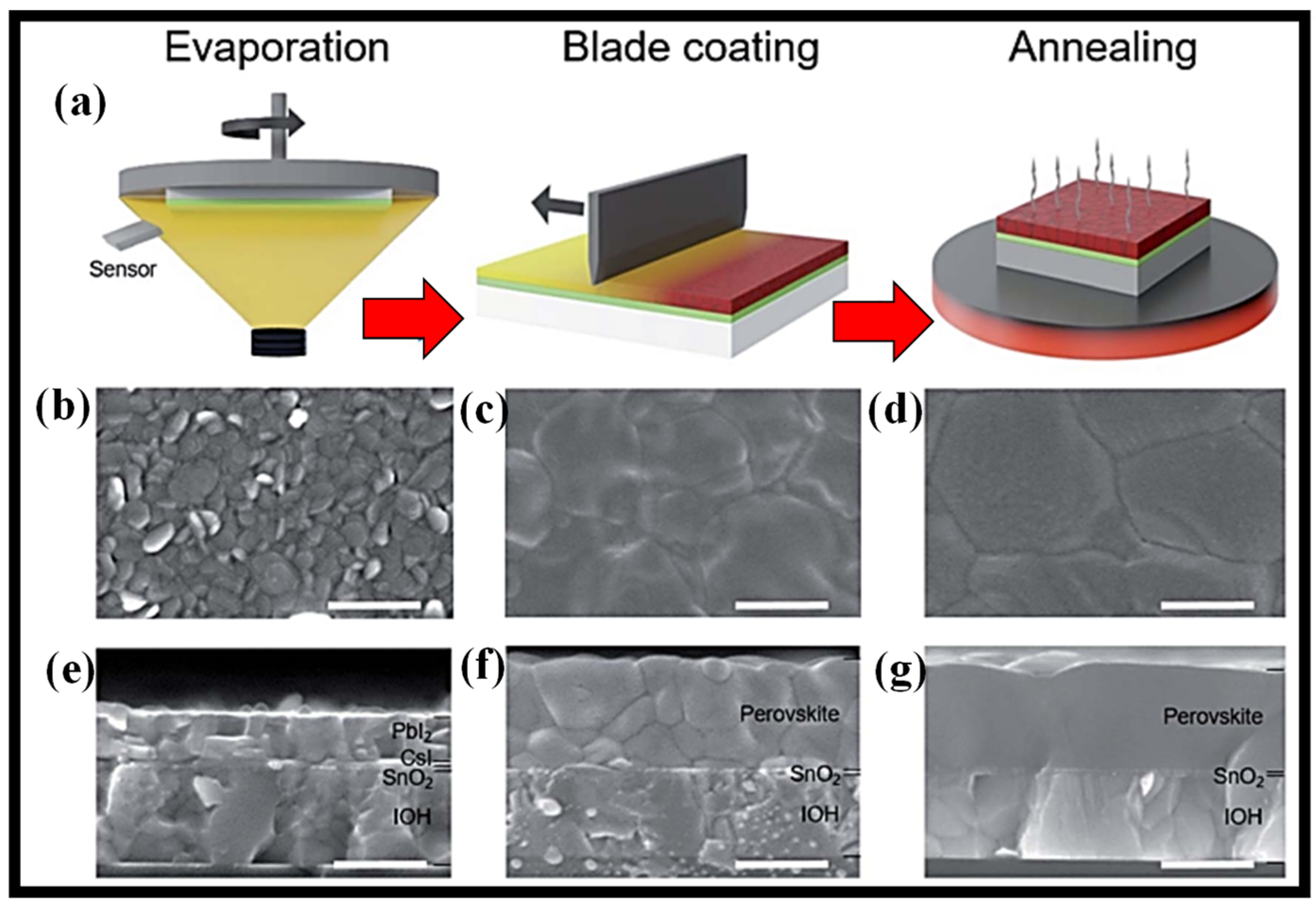
6. Blade-Coating
7. Other Thin-Film Deposition Methods
8. Author’s Opinion on Coating Methods and Concluding Remarks
Funding
Institutional Review Board Statement
Informed Consent Statement
Data Availability Statement
Acknowledgments
Conflicts of Interest
Abbreviations
| PVD | Physical vapor deposition |
| CVD | Chemical vapor deposition |
| FHD | Flame hydrolysis deposition |
| ALD | Atomic layer deposition |
| PSCs | Perovskite solar cells |
| PCE | Power conversion efficiency |
| SiO2:TiO2 | Silica-titania |
| BG | Bragg grating |
| WG | Waveguide |
| NIL | Nano-imprint lithography |
| SEM | Scanning electron microscopy |
| PVA | Polyvinyl alcohol |
| R-2-R | Roll-to-Roll |
| OHAM | Optimal homotopy asymptotic method |
| PDMS | Polydimethylsiloxane |
| PVDF | Polyvinylidene difluoride |
References
- Weinstein, S.; Ruschak, K. Coating flows. Annu. Rev. Fluid Mech. 2004, 36, 29–53. [Google Scholar] [CrossRef]
- Krebs, F. Fabrication and processing of polymer solar cells: A review of printing and coating techniques. Sol. Energy Mater. Sol. Cells 2009, 93, 394–412. [Google Scholar] [CrossRef]
- Konar, R.; Nessim, G. A mini-review focusing on ambient-pressure chemical vapor deposition (AP-CVD) based synthesis of layered transition metal selenides for energy storage applications. Mater. Adv. 2022, 3, 4471–4488. [Google Scholar] [CrossRef]
- Rossnagel, S. Thin film deposition with physical vapor deposition and related technologies. J. Vac. Sci. Technol. A 2003, 21, S74. [Google Scholar] [CrossRef]
- Johnson, R.; Hultqvist, A.; Bent, S. A brief review of atomic layer deposition: From fundamentals to applications. Materialstoday 2014, 17, 236–246. [Google Scholar] [CrossRef]
- Hong, Y.-S.; Lee, S.-R.; Kim, J.-H.; Lee, S.-Y. Application of a DLC-coating for improving hydrostatic piston shoe bearing performance under mixed friction conditions. Int. J. Precis. Eng. Manuf. 2015, 16, 335–341. [Google Scholar] [CrossRef]
- Tandon, P.; Boek, H. Experimental and theoretical studies of flame hydrolysis deposition process for making glasses for optical planar devices. J. Non-Cryst. Solids 2003, 317, 275–289. [Google Scholar] [CrossRef]
- Ruano, J.M.; Benoit, V.; Aitchison, J.S.; Cooper, J.M. Flame hydrolysis deposition of glass on silicon for the integration of optical and microfluidic devices. Anal. Chem. 2000, 72, 1093–1097. [Google Scholar] [CrossRef]
- Yang, Y.; Kim, K.-H.; Ong, J. A review on calcium phosphate coatings produced using a sputtering process: An alternative to plasma spraying. Biomaterials 2005, 26, 327–337. [Google Scholar] [CrossRef]
- Orudzhev, F.; Ramazanov, S.; Sobola, D.; Isaev, A.; Wang, C.; Magomedova, A.; Kadiev, M.; Kaviyarasu, K. Atomic layer deposition of mixed-layered aurivillius phase on TiO2 nanotubes: Synthesis, characterization and photoelectrocatalytic properties. Nanomaterials 2020, 10, 2183. [Google Scholar] [CrossRef]
- Dallaev, R.; Sobola, D.; Tofel, P.; Skvarenina, L.; Sedlak, P. Aluminum nitride nanofilms by atomic layer deposition using alternative precursors hydrazinium chloride and triisobutylaluminum. Coatings 2020, 10, 954. [Google Scholar] [CrossRef]
- Butt, M.A.; Solé, R.; Pujol, M.C.; Ródenas, A.; Lifante, G.; Choudhary, A.; Murugan, G.S.; Shepherd, D.P.; Wilkinson, J.S.; Aguiló, M.; et al. Fabrication of Y-splitters and Mach-Zehnder structures on (Yb, Nb):RbTiOPO4/RbTiOPO4 epitaxial layers by reactive ion etching. J. Lightwave Technol. 2015, 33, 1863–1871. [Google Scholar] [CrossRef]
- Butt, M.A.; Kozlova, E.S.; Khonina, S.N. Conditions of a single-mode rib channel waveguide based on dielectric TiO2/SiO2. Comput. Opt. 2017, 41, 494–498. [Google Scholar] [CrossRef]
- Middleman, S. Fundamentals of Polymer Processing; McGraw-Hill: New York, NY, USA, 1977. [Google Scholar]
- Bird, R.; Dai, G.; Yarusso, B. The rheology and flow of viscoplastic materials. Rev. Chem. Eng. 1983, 1, 1–70. [Google Scholar] [CrossRef]
- Jeong, J.; Lee, J.; Kim, H.; Kim, H.-K.; Na, S.-I. Ink-jet printed transparent electrode using nano-size indium tin oxide particles for organic photovoltaics. Sol. Energy Mater. Sol. Cells 2010, 94, 1840–1844. [Google Scholar] [CrossRef]
- Eom, S.; Park, H.; Mujawar, S.; Yoon, S.; Kim, S.-S.; Na, S.; Kang, S.-J.; Khim, D.; Kim, D.-Y.; Lee, S.-H. High efficiency polymer solar cells via sequential inkjet-printing of PEDOT:PSS and P3HT:PCBM inks with additives. Org. Electron. 2010, 11, 1516–1522. [Google Scholar] [CrossRef]
- Niu, X.; Li, N.; Chen, Q.; Zhou, H. Insights into large-scale fabrication methods in perovskite photovoltaics. Adv. Energy Sustain. Res. 2021, 2, 2000046. [Google Scholar] [CrossRef]
- Voigt, M.; Mackenzie, R.; King, S.; Yau, C.; Atienzar, P.; Dane, J.; Keivanidis, P.; Zadrazil, I.; Bradley, D.; Nelson, J. Gravure printing inverted organic solar cells: The influence of ink properties on film quality and device performance. Sol. Energy Mater. Sol. Cells 2012, 105, 77–85. [Google Scholar] [CrossRef]
- Kang, J.-W.; Kang, Y.-J.; Jung, S.; Song, M.; Kim, D.-G.; Kim, C.; Kim, S. Fully spray-coated inverted organic solar cells. Sol. Energy Mater. Sol. Cells 2012, 103, 76–79. [Google Scholar] [CrossRef]
- Girotto, C.; Rand, B.; Genoe, J.; Heremans, P. Exploring spray coating as a deposition technique for the fabrication of solution-processed solar cells. Sol. Energy Mater. Sol. Cells 2009, 93, 454–458. [Google Scholar] [CrossRef]
- Green, R.; Morfa, A. Performance of bulk heterojunction photovoltaic devices prepared by airbrush spray deposition. Appl. Phys. Lett. 2008, 92, 033301. [Google Scholar] [CrossRef]
- Karasinski, P.; Tyszkiewicz, C.; Domanowska, A.; Michalewicz, A.; Mazur, J. Low loss, long time stable sol-gel derived silica-titania waveguide films. Mater. Lett. 2015, 143, 5–7. [Google Scholar] [CrossRef]
- Brinker, C.J.; Frye, G.C.; Hurd, A.J.; Ashley, C.S. Fundamentals of sol-gel dip coating. Thin Solid Films 1991, 201, 97–108. [Google Scholar] [CrossRef]
- Brinker, C.J.; Ashley, C.S.; Cairncross, R.A.; Chen, K.S.; Hurd, A.J.; Reed, S.T.; Samuel, J.; Schunk, P.R.; Schwartz, R.W.; Scotto, C.S. Sol-gel derived ceramic films-fundamentals and applications. In Metallurgical and Ceramic Protective Coatings; Stern, K.H., Ed.; Springer: Dordrecht, The Netherlands, 1996. [Google Scholar]
- Jaglarz, J.; Dulian, P.; Karasinski, P.; Winkowski, P. Scattering phenomena in porous sol-gel-derived silica films. Coatings 2020, 10, 509. [Google Scholar] [CrossRef]
- Karasinski, P. Sol-gel derived optical waveguide films for planar sensors with phase modulation. Opt. Appl. 2004, 34, 467–475. [Google Scholar]
- Karasinski, P.; Tyszkiewicz, C.; Rogozinski, R. Rib waveguides based on the sol-gel derived SiO2:TiO2 films. Photonics Lett. Pol. 2010, 2, 40–42. [Google Scholar]
- Matsui, T.; Komatsu, K.; Sugihara, O.; Kaino, T. Simple process for fabricating a monolithic polymer optical waveguide. Opt. Lett. 2005, 30, 970–972. [Google Scholar] [CrossRef]
- Killinger, A.; Gantenbein, G.; Illy, S.; Ruess, T.; Weggen, J.; Martinez-Garcia, V. Plasma spraying of a microwave absorber coating for an RF dummy load. Coatings 2021, 11, 801. [Google Scholar] [CrossRef]
- Hongo, A.; Miyagi, M.; Kato, Y.; Suzumura, M.; Kubota, S.; Wang, Y.; Shimomura, T. Fabrication of dielectric-coated silver hollow glass waveguides for the infrared by liquid-flow coating method. In Proceedings of the Biomedical Fiber Optics, Photonics West, San Jose, CA, USA, 5 April 1996; Volume 2677. [Google Scholar]
- Faustini, M.; Louis, B.; Albouy, P.; Kuemmel, M.; Grosso, D. Preparation of sol−gel films by dip-coating in extreme conditions. J. Phys. Chem. C 2010, 114, 7637–7645. [Google Scholar] [CrossRef]
- Hakki, H.; Allahyari, S.; Rahemi, N.; Tasbihi, M. Surface properties, adherence, and photocatalytic activity of sol-gel dip-coated TiO2-ZnO films on glass plates. C. R. Chim. 2019, 22, 393–405. [Google Scholar] [CrossRef]
- Morais, D.; Boaventura, R.; Moreira, F.; Vilar, V. Advances in bromate reduction by heterogeneous photocatalysis: The use of a static mixer as photocatalyst support. Appl. Catal. B Environ. 2019, 249, 322–332. [Google Scholar] [CrossRef]
- Zarubica, A. Modified nanostructured titania based thin films in photocatalysis: Kinetic and mechanistic approach. React. Kinet. Mech. Catal. 2015, 115, 159–174. [Google Scholar] [CrossRef]
- Butt, M.; Tyszkiewicz, C.; Wojtasik, K.; Karasinski, P.; Kazmierczak, A.; Piramidowicz, R. Subwavelength grating waveguide structures proposed on the low-cost silica-titania platform for optical filtering and refractive index sensing applications. Int. J. Mol. Sci. 2022, 23, 6614. [Google Scholar] [CrossRef]
- Butt, M.; Kazmierczak, A.; Tyszkiewicz, C.; Karasinski, P.; Piramidowicz, R. Mode sensitivity exploration of silica-titania waveguide for refractive index sensing applications. Sensors 2021, 21, 7452. [Google Scholar] [CrossRef]
- Butt, M.; Tyszkiewicz, C.; Karasinski, P.; Zieba, M.; Hlushchenko, D.; Baraniecki, T.; Kazmierczak, A.; Piramidowicz, R.; Guzik, M.; Bachmatiuk, A. Development of a low-cost silica-titania optical platform for integrated photonics applications. Opt. Express 2022, 30, 23678. [Google Scholar] [CrossRef]
- Schroeder, H. Oxide layers deposited from organic solutions. In Physics of Thin Films: Advances in Research and Developments; Academic Press: New York, NY, USA; London, UK, 1969; pp. 87–141. [Google Scholar]
- Attia, S.M.; Wang, J.; Wu, G.; Shen, J.; Jianhua, M.A. Review on sol-gel derived coatings: Process, techniques and optical applications. J. Mater. Sci. Technol. 2002, 18, 211–217. [Google Scholar]
- Logan, M.N.; Prabakar, S.; Brinker, C.J. Sol-gel-derived silica films with tailored microstructures for applications requiring organic dyes. MRS Online Proc. Libr. 1994, 346, 115–120. [Google Scholar] [CrossRef] [Green Version]
- Fidalgo, A.; Ilharco, L.M. The defect structure of sol-gel-derived silica/polytetrahydrofuran hybrid films by FTIR. J. Non-Cryst. Solids 2001, 283, 144–154. [Google Scholar] [CrossRef]
- Parin, R.; Rigon, M.; Bortolin, S.; Martucci, A.; Col, D.D. Optimization of hybrid sol-gel coating for dropwise condensation of pure steam. Materials 2020, 13, 878. [Google Scholar] [CrossRef] [Green Version]
- Acosta, S.; Ayral, A.; Guizard, C.; Lecornec, C.; Passemard, G.; Moussavi, M. Sol-gel derived silica layers for low-k dielectrics applications. MRS Online Proc. Libr. 2000, 612, 5261. [Google Scholar] [CrossRef]
- Boudot, M.; Gaud, V.; Louarn, M.; Selmane, M.; Grosso, D. Sol-Gel based hydrophobic antireflective coatings on organic substrates: A detailed investigation of Ammonia Vapor Treatment (AVT). Chem. Mater. 2014, 26, 1822–1833. [Google Scholar] [CrossRef]
- Kim, T.; Song, K. Low-temperature preparation of superhydrophilic coatings using tetraethoxysilane and colloidal silica by sol-gel method. Colloids Surf. A Physicochem. Eng. Asp. 2022, 647, 129105. [Google Scholar] [CrossRef]
- Hasaneen, M.; Shalaby, M.; Yousif, N.; Diab, A.; Agammy, E. Structural and optical properties of transparent conducting oxide Cd1-xCrxO thin films prepared by the sol-gel dip-coating method. Mater. Sci. Eng. B 2022, 280, 115703. [Google Scholar] [CrossRef]
- Niazmand, M.; Maghsoudipour, A.; Alizadeh, M.; Khahpour, Z.; Kariminejad, A. Effect of dip coating parameters on microstructure and thickness of 8YSZ electrolyte coated on NiO-YSZ by sol-gel process for SOFCs applications. Ceram. Int. 2022, 48, 16091–16098. [Google Scholar] [CrossRef]
- Esfahani, M.; Eshaghi, A.; Bakhshi, S. Transparent hydrophobic, self-cleaning, anti-icing and anti-dust nano-structured silica based thin film on cover glass solar cell. J. Non-Cryst. Solids 2022, 583, 121479. [Google Scholar] [CrossRef]
- Beldjebli, O.; Bensaha, R.; Panneerselvam, P. Effect of both Sn doping and annealing temperature on the properties of dip-coated nanostructured TiO2 thin films. J. Inorg. Organomet. Polym. Mater. 2022, 32, 1624–1636. [Google Scholar] [CrossRef]
- Both, J.; Szabo, G.; Katona, G.; Muresan, L. Tannic acid reinforced sol-gel silica coatings for corrosion protecion of zinc substrates. Mater. Chem. Phys. 2022, 282, 125912. [Google Scholar] [CrossRef]
- Karasinski, P.; Tyszkiewicz, C.; Piramidowicz, R.; Kazmierczak, A. Development of integrated photonics based on SiO2:TiO2 sol-gel derived waveguide layers:state of the art, perspectives, prospective applications. Integr. Photonics Platf. Fundam. Res. Manuf. Appl. 2020, 11364, 1136414. [Google Scholar]
- Hermann, P.; Wildmann, D. Fabrication of planar dielectric waveguides with high optical damage threshold. IEEE J. Quantum Electron. 1983, 19, 1735–1738. [Google Scholar] [CrossRef]
- Lukosz, W.; Tiefenthaler, K. Embossing technique for fabricating integrated optical components in hard inorganic waveguiding materials. Opt. Lett. 1983, 8, 537–539. [Google Scholar] [CrossRef] [Green Version]
- Tiefenthaler, K.; Lukosz, W. Sensitivity of grating couplers as integrated-optical chemical sensors. J. Opt. Soc. Am. B 1989, 6, 209–220. [Google Scholar] [CrossRef]
- Clerc, D.; Lukosz, W. Direct immunosensing with an integrated-optical output grating coupler. Sens. Actuators B 1997, 40, 53–58. [Google Scholar] [CrossRef]
- Jiwei, Z.; Xi, Y.; Liangying, Z. Characterization and optical propagtion loss of sol-gel derived TiO2/SiO2 films. J. Phys. D Appl. Phys. 2000, 33, 3013–3017. [Google Scholar] [CrossRef]
- Tiefenthaler, K.; Briguet, V.; Buser, E.; Horisberger, M.; Lukosz, W. Preparation of planar optical SiO2-TiO2 and LiNbO3 waveguides with a dip coating method and embossing technique for fabricating grating couplers and channel waveguides. Proc. SPIE 1983, 401, 165–173. [Google Scholar]
- Chrysicopoulou, P.; Davazoglou, D.; Trapalis, C.; Kordas, G. Optical properties of SiO2-TiO2 sol-gel thin films. J. Mater. Sci. 2004, 39, 2835–2839. [Google Scholar] [CrossRef]
- Wang, X.; Wu, G.; Zhou, B.; Shen, J. Thermal annealing effect on optical properties of binary TiO2-SiO2 sol-gel coatings. Materials 2013, 6, 76–84. [Google Scholar] [CrossRef] [Green Version]
- Kermadi, S.; Agoudjil, N.; Sali, S.; Zougar, L.; Boumaour, M.; Broch, L.; Placido, F. Microstructure and optical dispersion characterization of nanocomposite sol–gel TiO2–SiO2 thin films with different compositions. Spectrochim. Acta Part A Mol. Biomol. Spectrosc. 2015, 145, 145–154. [Google Scholar] [CrossRef]
- Lukowiak, A.; Dylewicz, R.; Patela, S.; Strek, W.; Maruszewski, K. Optical properties of SiO2-TiO2 thin film waveguides obtained by the sol-gel method and their applications for sensing purposes. Opt. Mater. 2005, 27, 1501–1505. [Google Scholar] [CrossRef]
- Almeida, R.; Morais, P.; Vasconcelos, H. Optical loss mechanism in nanocomposite sol-gel planar waveguides. In Proceedings of the SPIE, Sol-Gel Optics IV, San Diego, CA, USA, 30 July–1 August 1997; pp. 296–303. [Google Scholar]
- Weisenbacht, L.; Zelinski, B. The attenuation of sol-gel waveguides measured as a function of wavelength and sample age. In Proceedings of the SPIE 2288 Sol-Gel Optics III, San Diego, CA, USA, 13 October 1994; pp. 630–639. [Google Scholar]
- Enami, Y. Fabricating 90 nm resolution structures in sol-gel silica optical waveguides for biosensor applications. J. Sens. 2017, 2017, 4198485. [Google Scholar] [CrossRef] [Green Version]
- Blankenburg, L.; Schultheis, K.; Schache, H.; Sensfuss, S.; Schrodner, M. Reel-to-reel wet coatings as an efficient up-scaling technique for the production of bulk-heterojunction polymer solar cells. Sol. Energy Mater. Sol. Cells 2009, 93, 476–483. [Google Scholar] [CrossRef]
- Emslie, A.; Bonner, F.; Peck, L. Flow of a viscous liquid on a rotating disk. J. Appl. Phys. 1958, 29, 858. [Google Scholar] [CrossRef]
- Huang, Y.-Y.; Chou, K.-S. Studies on the spin coating process of silica films. Ceram. Int. 2003, 29, 485–493. [Google Scholar] [CrossRef]
- Burmann, P.; Zornoza, B.; Tellez, C.; Coronas, J. Mixed matrix membranes comprising MOFs and porous silicate fillers prepared via span coating for gas separation. Chem. Eng. Sci. 2014, 107, 66–75. [Google Scholar] [CrossRef]
- Hashizume, M.; Kunitake, T. Preparation of self-supporting ultrathin films of titania by spin coating. Langmuir 2003, 19, 10172–10178. [Google Scholar] [CrossRef]
- Xie, Y.; Zabihi, F.; Eslamian, M. Fabrication of highly reproducible polymer solar cells using ultrasonic substrate vibration posttreatment. J. Photonics Energy 2016, 6, 045502. [Google Scholar] [CrossRef] [Green Version]
- Coyle, D.; Macosko, C.; Scriven, L. Film-splitting flows in forward roll coating. J. Fluid Mech. 1986, 171, 183–207. [Google Scholar] [CrossRef]
- Hintermaier, J.; White, R. The splitting of a water film between rotating rolls. TAPPI J. 1965, 48, 617–625. [Google Scholar]
- Benkreira, H.; Edwards, M.; Wilkinson, W. A semi-empirical model of the forward roll coating flow of Newtonian fluids. Chem. Eng. Sci. 1981, 36, 423–427. [Google Scholar] [CrossRef]
- Benkreira, H.; Edwards, M.; Wilkinson, W. Roll coating of purely viscous liquids. Chem. Eng. Sci. 1981, 36, 429–434. [Google Scholar] [CrossRef]
- Benkreira, H.; Edwards, M.; Wilkinson, W. Roll coating operations. J. Non-Newton. Fluid Mech. 1984, 14, 377–389. [Google Scholar] [CrossRef]
- Benkreira, H.; Patel, R.; Edwards, M.; Wilkinson, W. Classification and analyses of coating flows. J. Non-Newton. Fluid Mech. 1994, 54, 437–447. [Google Scholar] [CrossRef] [Green Version]
- Sofou, S.; Mitsoulis, E. Roll-over-web coating of pseudoplastic and viscoplastic sheets using the lubrication approximation. J. Plast. Film Sheet 2005, 21, 307–333. [Google Scholar] [CrossRef]
- Zahid, M.; Haroon, T.; Rana, M.; Siddiqui, A. Roll coating analysis of a third grade fluid. J. Plast. Film Sheet. 2017, 33, 72–91. [Google Scholar] [CrossRef]
- Zahid, M.; Rana, M.; Siddiqui, A. Roll coating analysis of a second-grade material. J. Plast. Film Sheet 2018, 34, 232–255. [Google Scholar] [CrossRef]
- Ali, N.; Atif, H.; Javed, M.; Sadiq, M. A theoretical analysis of roll-over-web coating of couple stress fluid. J. Plast. Film Sheet. 2018, 34, 43–59. [Google Scholar] [CrossRef] [Green Version]
- Gaskell, P.; Savage, M.; Summers, J.; Thompson, H. Modelling and analysis of meniscus roll coating. J. Fluid Mech. 1995, 298, 113–137. [Google Scholar] [CrossRef]
- Marinca, V.; Herisanu, N. Determination of periodic solutions for the motion of a particle on a rotating parabola by means of the optimal homotopy asymptotic method. J. Sound Vib. 2010, 329, 1450–1459. [Google Scholar] [CrossRef]
- Whitaker, J.; Kim, D.; Larson, B.; Zhang, F.; Berry, J.; Hest, M.; Zhu, K. Scalable slot-die coating of high performance perovskite solar cells. Sustain. Energy Fuels 2018, 2, 2442–2449. [Google Scholar] [CrossRef]
- Ahn, S.; Guo, L. High-speed roll-to-roll nanoimprint lithography on flexible plastic substrates. Adv. Mater. 2008, 20, 2044–2049. [Google Scholar] [CrossRef] [Green Version]
- Kim, Y.; Yang, T.-Y.; Suhonen, R.; Valimaki, M.; Maaninen, T.; Kemppainen, A.; Jeon, N.; Seo, J. Gravure-printed flexible perovskite solar cells: Toward roll-to-roll manufacturing. Adv. Sci. 2019, 6, 1802094. [Google Scholar] [CrossRef] [Green Version]
- Zi, W.; Jin, Z.; Liu, S.; Xu, B. Flexible perovskite solar cells based on green, continuous roll-to-roll printing technology. J. Energy Chem. 2018, 27, 971–989. [Google Scholar] [CrossRef] [Green Version]
- Jung, J.; Williams, S.; Jen, A.-Y. Low-temperature processed high-performance flexible perovskite solar cells via rationally optimized solvent washing treatments. RSC Adv. 2014, 4, 62971–62977. [Google Scholar] [CrossRef]
- Faisal, N.; Sellami, N.; Venturi, F.; Hussain, T.; Mallick, T.; Muhammad-Sukki, F.; Bishop, A.; Upadhyaya, H.; Katiyar, N.; Goel, S. Large-scale manufacturing route to metamaterial coatings using thermal spray techniques and their response to solar radiation. Emergent Mater. 2021, 4, 1619–1633. [Google Scholar] [CrossRef]
- Zhai, M.; Liu, Y.; Huang, J.; Hou, W.; Wu, S.; Zhang, B.; Li, H. Fabrication of TiO2-SrCO3 composite coatings by suspension plasma spraying: Microstructure and enhanced visible light photocatalytic performances. J. Spray Technol. 2020, 29, 1172–1182. [Google Scholar] [CrossRef]
- Gardon, M.; Guilemany, J. Milestones in functional titanium dioxide thermal spray coatings: A review. J. Spray Technol. 2014, 23, 577–595. [Google Scholar] [CrossRef] [Green Version]
- Li, F.; Lan, X.; Wang, L.; Kong, X.; Xu, P.; Tai, Y.; Liu, G.; Shi, J. An efficient photocatalyst coating strategy for intimately coupled photocatalysis and biodegradation (ICPB) powder spraying method. Chem. Eng. J. 2020, 383, 123092. [Google Scholar] [CrossRef]
- Santos, S.; Paulista, L.; Silva, T.; Dias, M.; Lopes, J.; Boaventura, R.; Vilar, V. Intensifying heterogeneous TiO2 photocatalysis for bromate reduction using the NETmix photoreactor. Sci. Total Environ. 2019, 664, 805–816. [Google Scholar] [CrossRef]
- Montecchio, F.; Chinungi, D.; Lanza, R.; Engvall, K. Surface treatments of metal supports for photocatalysis applications. Appl. Surf. Sci. 2017, 401, 283–296. [Google Scholar] [CrossRef]
- Bousmaha, M.; Bezzerrouk, M.; Kharroubi, B.; Akriche, A.; Naceur, R.; Hattabi, I.; Sandjak-Eddine, K. Enhanced photocatalysis by depositing ZnO thin film in the inner wall of glass tube. Optik 2019, 183, 727–731. [Google Scholar] [CrossRef]
- Susanna, G.; Salamandra, L.; Brown, T.; Carlo, A.; Brunetti, F.; Reale, A. Airbrush spray-coating of polymer bulk-heterojunction solar cells. Sol. Energy Mater. Sol. Cells 2011, 95, 1775–1778. [Google Scholar] [CrossRef]
- Park, S.-Y.; Kang, Y.-J.; Lee, S.; Kim, D.-G.; Kim, J.-K.; Kim, J.; Kang, J.-W. Spray-coated organic solar cells with large-area of 12.25 cm2. Sol. Energy Mater. Sol. Cells 2011, 95, 852–855. [Google Scholar] [CrossRef]
- Liu, S.; Zhang, X.; Zhang, L.; Xie, W. Ultrasonic spray coating polymer and small molecular organic film for organic light-emitting devices. Sci. Rep. 2016, 6, 37042. [Google Scholar] [CrossRef] [PubMed] [Green Version]
- Habibi, M.; Ahmadian-Yazdi, M.-R.; Eslamian, M. Optimization of spray coating for the fabrication of sequentially deposited planar perovskite solar cells. J. Photonics Energy 2017, 7, 022003. [Google Scholar] [CrossRef] [Green Version]
- Xiao, M.; Huang, F.; Huang, W.; Dkhissi, Y.; Zhu, Y.; Etheridge, J.; Gray-Weale, A.; Bach, U.; Cheng, Y.-B.; Spiccia, L. A fast deposition-crystallization procedure for highly efficient lead iodide perovskite thin-film solar cells. Angew. Chem. Int. Ed. Engl. 2014, 53, 9898–9903. [Google Scholar] [CrossRef] [PubMed]
- Jeon, N.; Noh, J.; Kim, Y.; Yang, W.; Ryu, S.; Seok, S. Solvent engineering for high-performance inorganic-organic hybrid perovskite solar cells. Nat. Mater. 2014, 13, 897–903. [Google Scholar] [CrossRef]
- Jeong, J.; Kim, M.; Seo, J.; Lu, H.; Ahlawat, P.; Mishra, A.; Yang, Y.; Hope, M.A.; Eickemeyer, F.T.; Kim, M.; et al. Pseudo-halide anion engineering for α-FAPbl3 perovskite solar cells. Nature 2021, 592, 381–385. [Google Scholar] [CrossRef]
- Qi, J.; Yang, Z.; Xingwang, Z.; Xiaolei, Y.; Yong, C.; Zema, C.; Qiufeng, Y.; Xingxing, L.; Zhigang, Y.; Jingbi, Y. Surface passivation of perovskite film for efficient solar cells. Nat. Photonics 2019, 13, 460–466. [Google Scholar]
- Gu, X.; Shaw, L.; Gu, K.; Toney, M.; Bao, Z. The meniscus-guided deposition of semiconducting polymers. Nat. Commun. 2018, 9, 534. [Google Scholar] [CrossRef]
- Li, D.; Zhang, D.; Lim, K.-S.; Hu, Y.; Rong, Y.; Mei, A.; Park, N.-G.; Han, H. A review on scaling up perovskite solar cells. Adv. Funct. Mater. 2021, 31, 2008621. [Google Scholar] [CrossRef]
- Deng, Y.; Peng, E.; Shao, Y.; Xiao, Z.; Dong, Z.; Huang, J. Scalable fabrication of efficient organolead trihalide perovskite solar cells with doctor-bladed active layers. Energy Environ. Sci. 2015, 8, 1544–1550. [Google Scholar] [CrossRef]
- Razza, S.; Giacomo, F.; Matteocci, F.; Cina, L.; Palma, A.L.; Casaluci, S.; Cameron, P.; D’Epifanio, A.; Licoccia, S.; Reale, A.; et al. Perovskite solar cells and large area modules (100 cm2) based on an air flow-assisted PbI2 blade coating deposition process. J. Power Sources 2015, 277, 286–291. [Google Scholar] [CrossRef]
- Vak, D.; Hwang, K.; Faulks, A.; Jung, Y.-S.; Clark, N.; Kim, D.-Y.; Wilson, G.; Watkins, S. Solar cells: 3D printer based slot-die coater as a lab-to-fab translation tool for solution-processed solar cells. Adv. Energy Mater. 2015, 5, 1401539. [Google Scholar] [CrossRef]
- Wei, Z.; Chen, H.; Yan, K.; Yang, S. Inkjet printing and instant chemical transformation of a CH3NH3PbI3/nanocarbon electrode and interface for planar perovskite solar cells. Angew. Chem. Int. Ed. Engl. 2014, 53, 13239–13243. [Google Scholar] [CrossRef] [PubMed]
- Heo, J.; Lee, M.; Jang, M.; Im, S. Highly efficient CH3NH3PbI3-x Clx mixed halide perovskite solar cells prepared by re-dissolution and crystal grain growth via spray coating. J. Mater. Chem. A 2016, 4, 17636–17642. [Google Scholar] [CrossRef]
- Schneider, A.; Traut, N.; Hamburger, M. Analysis and optimization of relevant parameters of blade coating and gravure printing processes for the fabrication of highly efficient organic solar cells. Sol. Energy Mater. Sol. Cells 2014, 126, 149–154. [Google Scholar] [CrossRef]
- Tsai, P.-T.; Tsai, C.-Y.; Wang, C.M.; Chang, Y.F.; Meng, H.-F.; Chen, Z.K.; Lin, H.W.; Zan, H.-W.; Horng, S.F.; Lai, Y.C.; et al. High-efficiency polymer solar cells by blade coating in chlorine-free solvents. Org. Electron. 2014, 15, 893–903. [Google Scholar] [CrossRef]
- Chang, Y.-H.; Tseng, S.-R.; Chen, C.-Y.; Meng, H.-F.; Chen, E.-C.; Horng, S.-F.; Hsu, C.-S. Polymer solar cell by blade coating. Oragnic Electron. 2009, 10, 741–746. [Google Scholar] [CrossRef]
- Mujahid, M.; Chen, C.; Hu, W.; Wang, Z.-K.; Duan, Y. Progress of high-throughput and low-cost flexible perovskite solar cells. Sol. RRL 2020, 4, 1900556. [Google Scholar] [CrossRef]
- Siegrist, S.; Yang, S.-C.; Gilshtein, E.; Sun, X.; Tiwari, A.; Fu, F. Triple-cation perovskite solar cells fabricated by a hybrid PVD/blade coating process using green solvents. J. Mater. Chem. A 2021, 9, 26680. [Google Scholar] [CrossRef]
- Jilani, A.; Abdel-wahab, M.S.; Hammad, A.H. Advance deposition techniques for thin film and coating. In Modern Technologies for Creating the Thin Film Systems and Coatings; IntechOpen: London, UK, 2017; pp. 137–149. [Google Scholar]
- Butt, M.A.; Tyszkiewicz, C.; Karasinski, P.; Zieba, M.; Kazmierczak, A.; Zdonczyk, M.; Duda, L.; Guzik, M.; Olszewski, J.; Martynkien, T.; et al. Optical thin films fabrication techniques—Towards a low-cost solution for the integrated photonic platform: A review of the current status. Materials 2022, 15, 4591. [Google Scholar] [CrossRef]
- Boolchandani, S.; Srivastava, S.; Vijay, Y.K. Preparation on InSe thin films by thermal evaporation method and their characterization: Structural, optical, and thermoelectrical properties. J. Nanotechnol. 2018, 2018, 9380573. [Google Scholar] [CrossRef] [Green Version]
- Ali, N.; Teixeira, J.A.; Addali, A.; Saeed, M.; Al-Zubi, F.; Sedaghat, A.; Bahzad, H. Deposition of stainless steel thin films: An electron beam physical vapour deposition approach. Materials 2019, 12, 571. [Google Scholar] [CrossRef] [PubMed] [Green Version]
- Ogugua, S.N.; Ntwaeaborwa, O.M.; Swart, H.C. Latest development on pulsed laser deposited thin films for advanced luminescence applications. Coatings 2020, 10, 1078. [Google Scholar] [CrossRef]
- Opel, M.; Geprags, S.; Althammer, M.; Brenninger, T.; Gross, R. Laser molecular beam epitaxy of ZnO thin films and heterostructures. J. Phys. D Appl. Phys. 2014, 47, 034002. [Google Scholar] [CrossRef] [Green Version]
- Martin, P.M. Handbook of deposition technologies for films and coatings. In Science, Applications and Technology, 3rd ed.; Elsevier Inc.: Amsterdam, The Netherlands, 2010; pp. 297–313. [Google Scholar]
- Randhawa, H.S.; Bunshah, R.F.; Brock, D.G.; Basol, B.M.; Stafsudd, O.M. Preparation of CuxS thin films by activated reactive evaporation technique. Sol. Energy Mater. 1982, 6, 445–453. [Google Scholar] [CrossRef]
- Woehrl, N.; Ochedowski, O.; Gottlieb, S.; Shibasaki, K.; Schulz, S. Plasma-enhanced chemical vapor deposition of graphene on copper substrates. AIP Adv. 2014, 4, 047128. [Google Scholar] [CrossRef] [Green Version]
- Cohen, A.; Patsha, A.; Mohapatra, P.K.; Kazes, M.; Ranganathan, K.; Houben, L.; Oron, D.; Ismach, A. Growth-etch metal-organic chemical vapor deposition approach of WS2 atomic layers. ACS Nano 2021, 15, 526–538. [Google Scholar] [CrossRef]
- Okada, H.; Baba, M.; Furukawa, M.; Yamane, K.; Sekiguchi, H.; Wakahara, A. Formation of SiO2 film by chemical vapor deposition enhanced by atomic species extracted from a surface-wave generated plasma. AIP Conf. Proc. 2017, 1807, 020006. [Google Scholar]
- Matsuura, Y.; Harrington, J.A. Hollow glass waveguides with three-layer dielectric coating fabricated by chemical vapor deposition. J. Opt. Soc. Am. A 1997, 14, 1255–1259. [Google Scholar] [CrossRef]
- Matsuura, Y.; Harrington, J.A. Infrared hollow glass waveguides fabricated by chemical vapor deposition. Opt. Lett. 1995, 20, 2078–2080. [Google Scholar] [CrossRef]
- Saha, J.K.; Bukke, R.N.; Mude, N.N.; Jang, J. Significant improvment of spray pyrolyzed ZnO thin film by precursor optimization for high mobility thin film transistors. Sci. Rep. 2020, 10, 8999. [Google Scholar] [CrossRef] [PubMed]
- Patil, G.E.; Kajale, D.D.; Gaikwad, V.B.; Jain, G.H. Spray pyrolysis deposition of nanostructured tin oxide thin films. Int. Sch. Res. Not. 2012, 2012, 275872. [Google Scholar] [CrossRef] [Green Version]
- Cho, J.; Hwang, S.; Ko, D.-H.; Chung, S. Transparent ZnO thin-film deposition by spray pyrolysis for high-performance metal-oxide field-effect transistors. Materials 2019, 12, 3423. [Google Scholar] [CrossRef] [PubMed] [Green Version]
- Filipovic, L.; Selberherr, S.; Mutinati, G.C.; Brunet, E.; Steinhauer, S.; Kock, A.; Teva, J.; Kraft, J.; Siegert, J.; Schrank, F. Methods of simulating thin film deposition using spray pyrolysis techniques. Microelectron. Eng. 2014, 117, 57–66. [Google Scholar] [CrossRef]
- Ramadhani, M.F.; Pasaribu, M.H.; Yuliarto, B. Fabrication of ZnO nanorod using spray-pyrolysis and chemical bath deposition method. AIP Conf. Proc. 2014, 1586, 74. [Google Scholar]
- Gong, K.; Du, F.; Xia, Z.; Durstock, M.; Dai, L. Nitrogen-doped carbon nanotube arrays with high electrocatalytic activity for oxygen reduction. Science 2009, 323, 760–764. [Google Scholar] [CrossRef] [Green Version]
- Wu, Z.; Chen, Z.; Du, X.; Logan, J.M.; Sippel, J.; Nikolou, M.; Kamaras, K.; Reynolds, J.R.; Tanner, D.B.; Hebard, A.F.; et al. Transparent, conductive carbon nanotube films. Science 2004, 305, 1273–1276. [Google Scholar] [CrossRef]
- De, S.; Higgins, T.M.; Lyons, P.E.; Doherty, E.M.; Nirmalraj, P.N.; Blau, W.J.; Boland, J.J.; Coleman, J.N. Silver nanowire networks as flexible, transparent, conducting films: Extremely high DC to optical conductivity ratios. ACS Nano 2009, 3, 1767–1774. [Google Scholar] [CrossRef]
- De, S.; Lyons, P.E.; Sorel, S.; Doherty, E.M.; King, P.J.; Blau, W.J.; Nirmalraj, P.N.; Boland, J.J.; Scardaci, V.; Joimel, J.; et al. Transparent, flexible and highly conductive thin films based on polymer-nanotube composites. ACS Nano 2009, 3, 714–720. [Google Scholar] [CrossRef]
- Abe, Y.; Tomuro, R.; Sano, M. Highly efficient direct current electrodeposition of single-walled carbon nanotubes in anhydrous solvents. Adv. Mater. 2005, 17, 2192–2194. [Google Scholar] [CrossRef]
- Li, X.; Cai, W.; An, J.; Kim, S.; Nah, J.; Yang, D.; Piner, R.; Velamakanni, A.; Jung, I.; Tutuc, E.; et al. Large-area synthesis of high-quality and uniform graphene films on copper foils. Science 2009, 324, 1312–1314. [Google Scholar] [CrossRef] [PubMed] [Green Version]
- Zhang, D.; Ryu, K.; Liu, X.; Polikarpov, E.; Ly, J.; Tompson, M.E.; Zhou, C. Transparent, conductive and flexible nanotube films and their application in organic light-emitting diodes. Nano Lett. 2006, 6, 1880–1886. [Google Scholar] [CrossRef] [PubMed]
- Song, J.; Kam, F.Y.; Png, R.Q.; Seah, W.L.; Zhuo, J.M.; Lim, G.K.; Ho, P.K.; Chua, L.L. A general method for transferring graphene onto soft surfaces. Nat. Nanotechnol. 2013, 8, 356–362. [Google Scholar] [CrossRef]
- Eda, G.; Fanchina, G.; Chhowalla, M. Large-area ultrathin films of reduced graphene oxide as a transparent and flexible electronic material. Nat. Nanotechnol. 2008, 3, 270–274. [Google Scholar] [CrossRef] [PubMed]
- Zhang, Y.; Magan, J.; Blau, W. A general strategy for hybrid thin film fabrication and transfer onto arbitrary substrates. Sci. Rep. 2014, 4, 4822. [Google Scholar] [CrossRef] [Green Version]
- Jagadeesan, S.; Lim, J.; Choi, K.; Doh, Y. Hybrid multilayer thin-film fabrication by atmospheric deposition process for enhancing the barrier performance. J. Coat. Technol. Res. 2018, 15, 1391–1399. [Google Scholar] [CrossRef]


Publisher’s Note: MDPI stays neutral with regard to jurisdictional claims in published maps and institutional affiliations. |
© 2022 by the author. Licensee MDPI, Basel, Switzerland. This article is an open access article distributed under the terms and conditions of the Creative Commons Attribution (CC BY) license (https://creativecommons.org/licenses/by/4.0/).
Share and Cite
Butt, M.A. Thin-Film Coating Methods: A Successful Marriage of High-Quality and Cost-Effectiveness—A Brief Exploration. Coatings 2022, 12, 1115. https://doi.org/10.3390/coatings12081115
Butt MA. Thin-Film Coating Methods: A Successful Marriage of High-Quality and Cost-Effectiveness—A Brief Exploration. Coatings. 2022; 12(8):1115. https://doi.org/10.3390/coatings12081115
Chicago/Turabian StyleButt, Muhammad A. 2022. "Thin-Film Coating Methods: A Successful Marriage of High-Quality and Cost-Effectiveness—A Brief Exploration" Coatings 12, no. 8: 1115. https://doi.org/10.3390/coatings12081115