
Structure and Electrical Properties of Zirconium-Aluminum-Oxide Films Engineered by Atomic Layer Deposition

 , , , , , ,
Abstract
:1. Introduction
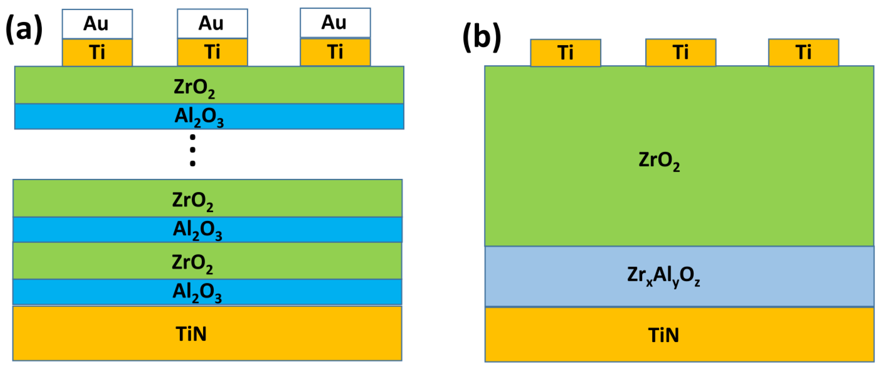
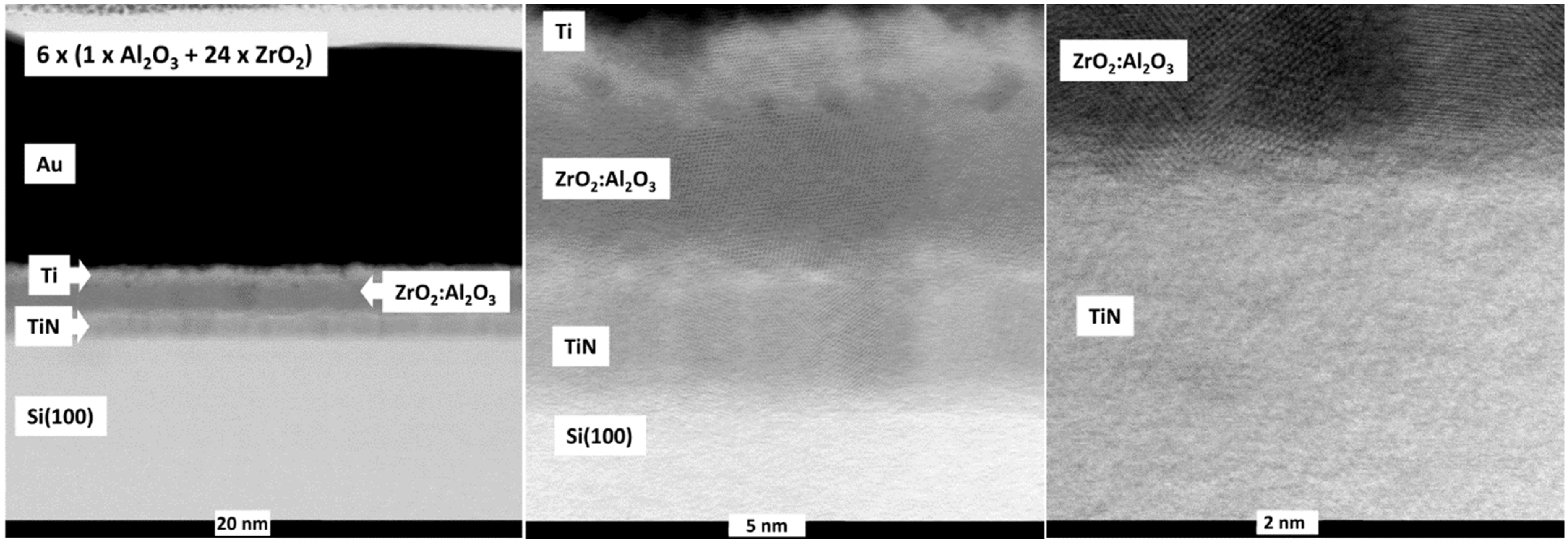
2. Materials and Methods
3. Results and Discussion
3.1. Composition
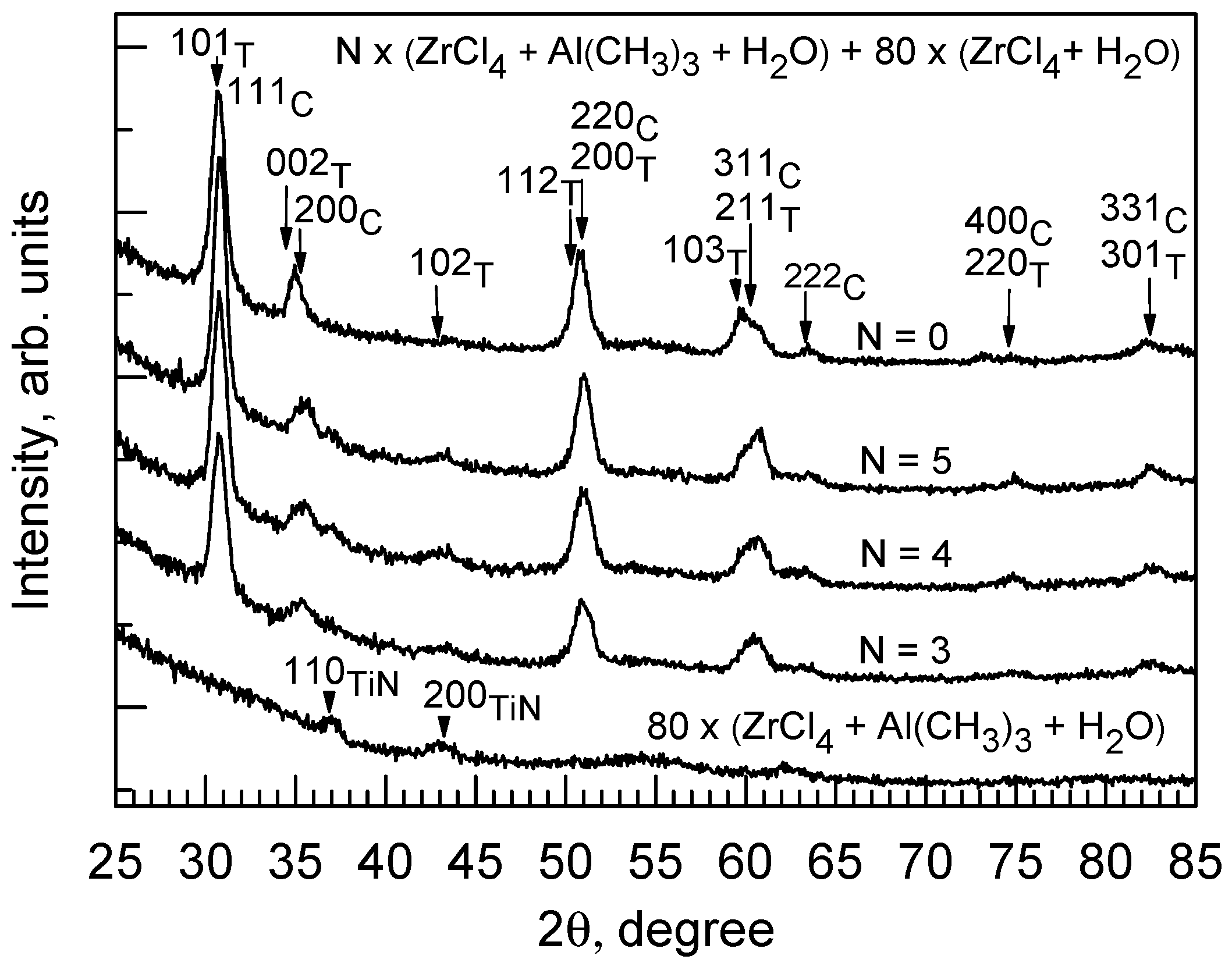
3.2. Structure
3.3. Dielectric Properties
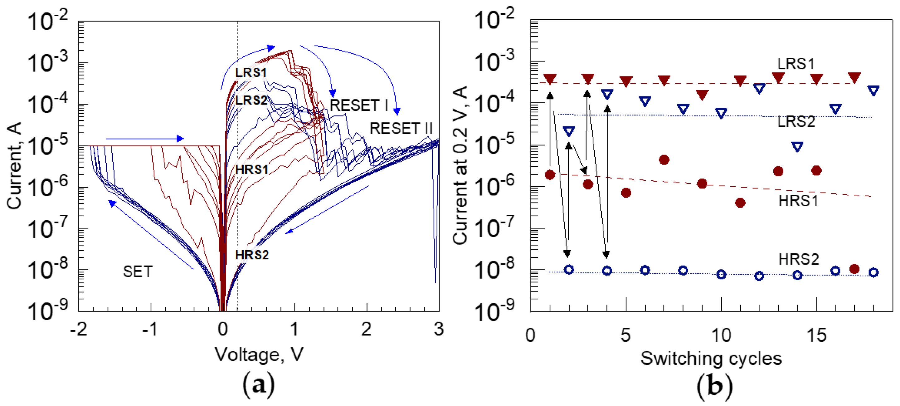
3.4. Resistive Switching Performance
4. Conclusions
Author Contributions
Funding
Institutional Review Board Statement
Informed Consent Statement
Data Availability Statement
Acknowledgments
Conflicts of Interest
References
- Kil, D.-S.; Song, H.-S.; Lee, K.-J.; Hong, K.; Kim, J.-H.; Park, K.-S.; Yeom, S.-J.; Roh, J.-S.; Kwak, N.-J.; Sohn, H.-C.; et al. Development of new TiN/ZrO2/Al2O3/ZrO2/TiN capacitors extendable to 45 nm generation DRAMs replacing HfO2 based dielectrics. In Proceedings of the IEEE 2006 Symposium on VLSI Technology, Honolulu, HI, USA, 13–15 June 2006. [Google Scholar] [CrossRef]
- Cho, H.J.; Kim, Y.D.; Park, D.S.; Lee, E.; Park, C.H.; Jang, J.S.; Lee, K.B.; Kim, H.W.; Ki, Y.J.; Han, I.K.; et al. New TIT capacitor with ZrO2/Al2O3/ZrO2 dielectrics for 60 nm and below DRAMs. Solid State Electr. 2007, 51, 1529–1533. [Google Scholar] [CrossRef]
- Martin, D.; Grube, M.; Weinreich, W.; Müller, J.; Weber, W.M.; Schröder, U.; Riechert, H.; Mikolajick, T. Mesoscopic analysis of leakage current suppression in ZrO2/Al2O3/ZrO2 nano-laminates. J. Appl. Phys. 2013, 113, 194103. [Google Scholar] [CrossRef]
- Pešić, M.; Knebel, S.; Cho, K.; Jung, C.; Chang, J.; Lim, H.; Kolomiiets, N.; Afanas’ev, V.V.; Mikolajick, T.; Schroeder, U. Conduction barrier offset engineering for DRAM capacitor scaling. Solid-State Electr. 2016, 115, 133–139. [Google Scholar] [CrossRef]
- Zahoor, F.; Zainal, T.; Zulkifli, A.; Khanday, F.A. Resistive random access memory (RRAM): An overview of materials, switching mechanism, performance, multilevel cell (mlc) storage, modeling, and applications. Nanoscale Res. Lett. 2020, 15, 90. [Google Scholar] [CrossRef] [PubMed]
- Sun, K.; Chen, J.; Yan, X. The future of memristors: Materials engineering and neural networks. Adv. Funct. Mater. 2021, 31, 2006773. [Google Scholar] [CrossRef]
- Shi, T.; Wang, R.; Wu, Z.; Sun, Y.; An, J.; Liu, Q. A review of resistive switching devices: Performance, improvement, characterization, and applications. Small Struct. 2021, 2, 2000109. [Google Scholar] [CrossRef]
- Panda, D.; Tseng, T.-Y. Growth, dielectric properties, and memory device applications of ZrO2 thin films. Thin Solid Films 2013, 531, 1–20. [Google Scholar] [CrossRef]
- Awais, M.N.; Kim, H.C.; Doh, Y.H.; Choi, K.H. ZrO2 flexible printed resistive (memristive) switch through electrohydrodynamic printing process. Thin Solid Films 2013, 536, 308–312. [Google Scholar] [CrossRef]
- Kärkkänen, I.; Shkabko, A.; Heikkilä, M.; Niinistö, J.; Ritala, M.; Leskelä, M.; Hoffmann-Eifert, S.; Waser, R. Study of atomic layer deposited ZrO2 and ZrO2/TiO2 films for resistive switching application. Phys. Status Sol. A 2014, 211, 301–309. [Google Scholar] [CrossRef]
- Parreira, P.; Paterson, G.W.; McVitie, S.; MacLaren, D.A. Stability, bistability and instability of amorphous ZrO2 resistive memory devices. J. Phys. D Appl. Phys. 2016, 49, 095111. [Google Scholar] [CrossRef]
- Abbas, Y.; Han, I.S.; Sokolov, A.S.; Jeon, Y.-R.; Choi, C. Rapid thermal annealing on the atomic layer deposited zirconia thin film to enhance resistive switching characteristics. J. Mater. Sci. Mater. Electron. 2020, 31, 903–909. [Google Scholar] [CrossRef]
- Wei, X.; Huang, H.; Ye, C.; Wei, W.; Zhou, H.; Chen, Y.; Zhang, R.; Zhang, L.; Xia, Q. Exploring the role of nitrogen incorporation in ZrO2 resistive switching film for enhancing the device performance. J. Alloys Compd. 2019, 775, 1301–1306. [Google Scholar] [CrossRef]
- Huang, R.; Yan, X.; Morgan, K.A.; Charlton, M.D.B.; de Groot, C.H. Selection by current compliance of negative and positive bipolar resistive switching behaviour in ZrO2−x/ZrO2 bilayer memory. J. Phys. D Appl. Phys. 2017, 50, 175101. [Google Scholar] [CrossRef]
- Liu, H.-C.; Tang, X.-G.; Liu, Q.-X.; Jiang, Y.-P.; Li, W.-H.; Guo, X.-B.; Tang, Z.-H. Bipolar resistive switching behavior and conduction mechanisms of composite nanostructured TiO2 /ZrO2 thin film. Ceram. Int. 2020, 46, 21196. [Google Scholar] [CrossRef]
- Fu, L.; Li, Y.; Han, G.; Gao, X.; Chen, C.; Yuan, P. Stable resistive switching characteristics of ZrO2 -based memory device with low-cost. Microelectron. Eng. 2017, 172, 26–29. [Google Scholar] [CrossRef]
- Seidl, H.; Gutsche, M.; Schroeder, U.; Birner, A.; Hecht, T.; Jakschik, S.; Luetzen, J.; Kerber, M.; Kudelka, S.; Popp, T.; et al. A fully integrated Al2O3 trench capacitor DRAM for sub-100 nm technology. In Proceedings of the IEEE Digest: International Electron Devices Meeting, San Francisco, CA, USA, 8–11 December 2002. [Google Scholar] [CrossRef]
- Vishwanath, S.K.; Woo, H.; Jeon, S. Enhancement of resistive switching properties in Al2O3 bilayer-based atomic switches: Multilevel resistive switching. Nanotechnology 2018, 29, 235202. [Google Scholar] [CrossRef]
- Huang, X.-D.; Li, Y.; Li, H.-Y.; Xue, K.-H.; Wang, X.; Miao, X.-S. Forming-free, fast, uniform, and high endurance resistive switching from cryogenic to high temperatures in W/AlOx/Al2O3/Pt bilayer memristor. IEEE Electron Device Lett. 2020, 41, 549–552. [Google Scholar] [CrossRef]
- Jang, J.; Choi, H.-H.; Paik, S.H.; Kim, J.K.; Chung, S.; Park, J.H. Highly improved switching properties in flexible aluminum oxide resistive memories based on a multilayer device structure. Adv. Electron. Mater. 2018, 4, 1800355. [Google Scholar] [CrossRef]
- Kim, S.; Choi, Y.-K. Resistive switching of aluminum oxide for flexible memory. Appl. Phys. Lett. 2008, 92, 223508. [Google Scholar] [CrossRef]
- Mahata, C.; Kang, M.; Kim, C. Multi-level analog resistive switching characteristics in tri-layer HfO2/Al2O3/HfO2 based memristor on ITO electrode. Nanomaterials 2020, 10, 2069. [Google Scholar] [CrossRef]
- Castán, H.; Dueñas, S.; Kukli, K.; Kemell, M.; Ritala, M.; Leskelä, M. Study of the influence of the dielectric composition of Al/Ti/ZrO2:Al2O3/TiN/Si/Al structures on the resistive switching behavior for memory applications. ECS Trans. 2018, 85, 143. [Google Scholar] [CrossRef]
- Kukli, K.; Kemell, M.; Castán, H.; Dueñas, S.; Seemen, H.; Rähn, M.; Link, J.; Stern, R.; Heikkilä, M.J.; Ritala, M.; et al. Atomic layer deposition and performance of ZrO2-Al2O3 thin films. ECS J. Solid State Sci. Technol. 2018, 7, P287–P294. [Google Scholar] [CrossRef]
- Lin, C.-C.; Su, C.-T.; Chang, C.-L.; Wu, H.-Y. Resistive switching behavior of Al/Al2O3/ZrO2/Al structural device for flexible nonvolatile memory application. IEEE Trans. Magn. 2014, 50, 3000704. [Google Scholar] [CrossRef]
- Tsai, T.-L.; Chang, H.-Y.; Lou, J.J.-C.; Tseng, T.-Y. A high performance transparent resistive switching memory made from ZrO2/AlON bilayer structure. Appl. Phys. Lett. 2016, 108, 153505. [Google Scholar] [CrossRef]
- Arroval, T.; Aarik, L.; Rammula, R.; Kruusla, V.; Aarik, J. Effect of substrate-enhanced and inhibited growth on atomic layer deposition and properties of aluminum–titanium oxide films. Thin Solid Films 2016, 600, 119–125. [Google Scholar] [CrossRef]
- Granneman, E.; Fischer, P.; Pierreux, D.; Terhorst, H.; Zagwijn, P. Batch ALD: Characteristics, comparison with single wafer ALD, and examples. Surf. Coat. Technol. 2017, 201, 8899–8907. [Google Scholar] [CrossRef]
- Zagwijn, P.; Verweij, W.; Pierreux, D.; Adjeroud, N.; Bankras, R.; Oosterlaken, E.; Snijders, G.J.; van den Hout, M.; Fischer, P.; Wilhelm, R.; et al. Novel batch titanium nitride CVD process for advanced metal electrodes. ECS Trans. 2008, 13, 459–464. [Google Scholar] [CrossRef]
- Lee, S.S.; Baik, J.Y.; An, K.-S.; Suh, Y.D.; Oh, J.-H.; Kim, Y. Reduction of incubation period by employing OH-terminated Si(001) substrates in the atomic layer deposition of Al2O3. J. Phys. Chem. B 2004, 108, 15128–15132. [Google Scholar] [CrossRef]
- Aarik, J.; Aidla, A.; Kikas, A.; Käämbre, T.; Rammula, R.; Ritslaid, P.; Uustare, T.; Sammelselg, V. Effects of precursors on nucleation in atomic layer deposition of HfO2. Appl. Surf. Sci. 2013, 230, 292–300. [Google Scholar] [CrossRef]
- Zhao, C.; Richard, O.; Bender, H.; Caymax, M.; De Gendt, S.; Heyns, M.; Young, E.; Roebben, G.; Van Der Biest, O.; Haukka, S. Miscibility of amorphous ZrO2–Al2O3 binary alloy. Appl. Phys. Lett. 2002, 80, 2374–2376. [Google Scholar] [CrossRef]
- Gehensel, R.J.; Zierold, R.; Schaan, G.; Shang, G.; Petrov, A.Y.; Eich, M.; Blick, R.; Krekeler, T.; Janssen, R.; Furlan, K.P. Improved thermal stability of zirconia macroporous structures via homogeneous aluminum oxide doping and nanostructuring using atomic layer deposition. J. Eur. Ceram. Soc. 2021, 41, 4302–4312. [Google Scholar] [CrossRef]
- Ravichandran, A.T.; Pushpa, K.C.S.; Ravichandran, K.; Karthika, K.; Nagabhushana, B.M.; Mantha, S.; Swaminathan, K. Effect of Al doping on the structural and optical properties of ZrO2 nanopowders synthesized using solution combustion method. Superlattices Microstruct. 2014, 75, 533–542. [Google Scholar] [CrossRef]
- Balakrishnan, G.; Sairam, T.N.; Reddy, V.R.; Kuppusami, P.; Song, J.I. Microstructure and optical properties of Al2O3/ZrO2 nano multilayer thin films prepared by pulsed laser deposition. Mater. Chem. Phys. 2013, 140, 60–65. [Google Scholar] [CrossRef]
- Århammar, C.; Araújo, C.M.; Ahuja, R. Energetics of Al doping and intrinsic defects in monoclinic and cubic zirconia: First-principles calculations. Phys. Rev. B 2009, 80, 115208. [Google Scholar] [CrossRef]
- Zhu, Y.-L.; Xue, K.-H.; Cheng, X.-M.; Qiao, C.; Yuan, J.-H.; Li, L.-H.; Miao, X.-S. Uniform and robust TiN/HfO2/Pt memristor through interfacial Al-doping engineering. Appl. Surf. Sci. 2021, 550, 149274. [Google Scholar] [CrossRef]
- Ismail, M.; Mahata, C.; Kim, S. Forming-free Pt/Al2O3/HfO2/HfAlOx/TiN memristor with controllable multilevel resistive switching and neuromorphic characteristics for artificial synapse. J. Alloys Compd. 2021, 892, 162141. [Google Scholar] [CrossRef]
- Fairley, N. CasaXPS: Processing Software for XPS, AES, SIMS and More (Casa Software Ltd., 2018). Available online: http://www.casaxps.com (accessed on 28 January 2021).
- Tanuma, S.; Powell, C.J.; Penn, D.R. Calculations of electron inelastic mean free paths. V. Data for 14 organic compounds over the 50–2000 eV range. Surf. Interf. Anal. 1994, 21, 165–176. [Google Scholar] [CrossRef]
- Kukli, K.; Ritala, M.; Aarik, J.; Uustare, T.; Leskelä, M. Influence of growth temperature on properties of zirconium dioxide films grown by atomic layer deposition. J. Appl. Phys. 2002, 92, 1833–1840. [Google Scholar] [CrossRef]
- Ritala, M.; Leskelä, M. Zirconium dioxide thin films deposited by ALE using zirconium tetrachloride as precursor. Appl. Surf. Sci. 1994, 75, 333–340. [Google Scholar] [CrossRef]
- Siimon, H.; Aarik, J. Thickness profiles of thin films caused by secondary reactions in flow-type atomic layer deposition reactors. J. Phys. D Appl. Phys. 1997, 30, 1725–1728. [Google Scholar] [CrossRef]
- Arroval, T.; Aarik, L.; Rammula, R.; Aarik, J. Growth of TixAl1−xOy films by atomic layer deposition using successive supply of metal precursors. Thin Solid Films 2015, 591, 276–284. [Google Scholar] [CrossRef]
- Aarik, J.; Aidla, A.; Mändar, H.; Uustare, T.; Sammelselg, V. Growth kinetics and structure formation of ZrO2 thin films in chloride-based atomic layer deposition process. Thin Solid Films 2002, 408, 97–103. [Google Scholar] [CrossRef]
- Han, J.H.; Gao, G.; Widjaja, Y.; Garfunkel, E.; Musgrave, C.B. A quantum chemical study of ZrO2 atomic layer deposition growth reactions on the SiO2 surface. Surf. Sci. 2004, 550, 199–212. [Google Scholar] [CrossRef]
- Jeloaica, L.; Estève, A.; Rouhani, M.D.; Estève, D. Density functional theory study of HfCl4, ZrCl4, and Al(CH3)3 decomposition on hydroxylated SiO2: Initial stage of high-k atomic layer deposition. Appl. Phys. Lett. 2003, 83, 542–544. [Google Scholar] [CrossRef]
- Rawat, A.; Meer, M.; Surana, V.K.; Pendem, V.; Garigapati, N.S.; Yadav, Y.; Ganguly, S.; Saha, D. Thermally grown TiO2 and Al2O3 for GaN-based MOS-HEMTs. IEEE Trans. Electron Devices 2018, 65, 3725–3731. [Google Scholar] [CrossRef]
- Lee, J.S.; Kim, H.S.; Park, N.-K.; Lee, T.J.; Kang, M. Low temperature synthesis of α-alumina from aluminum hydroxide hydrothermally synthesized using [Al(C2O4)x(OH)y] complexes. Chem. Eng. J. 2013, 230, 351–360. [Google Scholar] [CrossRef]
- Crist, B.V. Handbooks of Monochromatic XPS Spectra, Volume 2—Commercially Pure Binary Oxides and a few Common Carbonates and Hydroxides; XPS International LLC.: Mountain View, CA, USA, 2005; Available online: https://xpslibrary.com/wp-content/uploads/----PDFs/Vol-2-XPS-of-Binary-Oxides.pdf (accessed on 12 January 2022).
- Tao, N.; Liu, J.; Xu, Y.; Feng, Y.; Wang, Y.; Liu, W.; Wang, H.; Lv, J. Highly selective and stable ZrO2–Al2O3 for synthesis of dimethyl carbonate in reactive distillation. Chem. Pap. 2020, 74, 3503–3515. [Google Scholar] [CrossRef]
- Zhao, X.; Vanderbilt, D. Phonons and lattice dielectric properties of zirconia. Phys. Rev. B 2002, 65, 075105. [Google Scholar] [CrossRef] [Green Version]
- Vanderbilt, D.; Zhao, X.; Ceresoli, D. Structural and dielectric properties of crystalline and amorphous ZrO2. Thin Solid Films 2005, 486, 125–128. [Google Scholar] [CrossRef]
- Xie, J.; Zhu, Z.; Tao, H.; Zhou, S.; Liang, Z.; Li, Z.; Yao, R.; Wang, Y.; Ning, H.; Peng, J. Research progress of high dielectric constant zirconia-based materials for gate dielectric application. Coatings 2020, 10, 698. [Google Scholar] [CrossRef]
- Krupka, J.; Geyer, R.G.; Kuhn, M.; Hinken, J.H. Dielectric properties of single crystals of Al2O3, LaAlO3, NdGaO3, SrTiO3, and MgO at cryogenic temperatures. IEEE Trans. Microw. Theor. Tech. 1994, 42, 1886–1890. [Google Scholar] [CrossRef]
- Groner, M.D.; Elam, J.W.; Fabreguette, F.H.; George, S.M. Electrical characterization of thin Al2O3 films grown by atomic layer deposition on silicon and various metal substrates. Thin Solid Films 2002, 413, 186–197. [Google Scholar] [CrossRef]
- Wu, J.Z.; Acharya, J.; Goul, R. In vacuo atomic layer deposition and electron tunneling characterization of ultrathin dielectric films for metal/insulator/metal tunnel junctions. J. Vac. Sci. Technol. A 2020, 38, 040802. [Google Scholar] [CrossRef]
- Link, G.; Heidinger, R. Dielectric property measurements of ZrO2-strengthened Al2O3. J. Appl. Phys. 1997, 81, 3257–3262. [Google Scholar] [CrossRef]
- Zhu, M.; Chen, P.; Fu, R.K.Y.; Liu, W.; Lin, C.; Chu, P.K. Microstructure and electrical properties of Al2O3–ZrO2 composite films for gate dielectric applications. Thin Solid Films 2005, 476, 312–316. [Google Scholar] [CrossRef]
- Peng, J.; Wei, J.; Zhu, Z.; Ning, H.; Cai, W.; Lu, K.; Yao, R.; Tao, H.; Zheng, Y.; Lu, X. Properties-adjustable alumina-zirconia nanolaminate dielectric fabricated by spin-coating. Nanomaterials 2017, 7, 419. [Google Scholar] [CrossRef] [Green Version]
- Liang, Z.; Zhou, S.; Cai, W.; Fu, X.; Ning, H.; Chen, J.; Yuan, W.; Zhu, Z.; Yao, R.; Peng, J. Zirconium-aluminum-oxide dielectric layer with high dielectric and relatively low leakage prepared by spin-coating and the application in thin-film transistor. Coatings 2020, 10, 282. [Google Scholar] [CrossRef] [Green Version]
- Chen, X.; Cheng, Y.; Wu, K.; Meng, Y.; Wu, S. Calculation of dielectric constant of two-phase disordered composites by using FEM. In Proceedings of the Conference Record of the 2008 IEEE International Symposium on Electrical Insulation, Vancouver, BC, Canada, 9–12 June 2008. [Google Scholar] [CrossRef]
- Sihvola, A. Homogenization principles and effect of mixing on dielectric behavior. Photonics Nanostruct. Fundam. Appl. 2013, 11, 364–373. [Google Scholar] [CrossRef] [Green Version]
- Waggoner, T.; Triska, J.; Hoshino, K.; Wager, J.F.; Conley, J.F., Jr. Zirconium oxide-aluminum oxide nanolaminate gate dielectrics for amorphous oxide semiconductor thin-film transistors. J. Vac. Sci. Technol. B 2011, 29, 04D115. [Google Scholar] [CrossRef] [Green Version]
- Zhu, B.; Wu, X.; Liu, W.-J.; Ding, S.-J.; Zhang, D.W.; Fan, Z. Dielectric enhancement of atomic layer-deposited Al2O3/ZrO2/Al2O3 MIM capacitors by microwave annealing. Nanoscale Res. Lett. 2019, 14, 53. [Google Scholar] [CrossRef]
- Walczyk, C.; Wenger, C.; Sohal, R.; Lukosius, M.; Fox, A.; Dąbrowski, J.; Wolansky, D.; Tillack, B.; Müssig, H.-J.; Schroeder, T. Pulse-induced low-power resistive switching in HfO2 metal-insulator-metal diodes for nonvolatile memory applications. J. Appl. Phys. 2009, 105, 114103. [Google Scholar] [CrossRef]
- Liu, M.; Abid, Z.; Wang, W.; He, X.; Liu, Q.; Guan, W. Multilevel resistive switching with ionic and metallic filaments. Appl. Phys. Lett. 2009, 94, 233106. [Google Scholar] [CrossRef] [Green Version]
- Huang, R.; Yan, X.; Ye, S.; Kashtiban, R.; Beanland, R.; Morgan, K.A.; Charlton, M.D.B.; de Groot, C.H. Compliance-free ZrO2/ZrO2 − x/ZrO2 resistive memory with controllable interfacial multistate switching behaviour. Nanoscale Res. Lett. 2017, 12, 384. [Google Scholar] [CrossRef] [PubMed] [Green Version]
- Yildirim, H.; Pachter, R. Extrinsic dopant effects on oxygen vacancy formation energies in ZrO2 with implication for memristive device performance. ACS Appl. Electron. Mater. 2019, 1, 467–477. [Google Scholar] [CrossRef]
- Pey, K.L.; Thamankar, R.; Sen, M.; Bosman, M.; Raghavan, N.; Shubhakar, K. Understanding the switching mechanism in RRAM using in-situ TEM. In Proceedings of the 2016 IEEE Silicon Nanoelectronics Workshop (SNW), Honolulu, HI, USA, 12–13 June 2016. [Google Scholar] [CrossRef]
- Kwon, D.-H.; Kim, K.M.; Jang, J.H.; Jeon, J.M.; Lee, M.H.; Kim, G.H.; Li, X.-S.; Park, G.-S.; Lee, B.; Han, S.; et al. Atomic structure of conducting nanofilaments in TiO2 resistive switching memory. Nat. Nanotechnol. 2010, 5, 148–153. [Google Scholar] [CrossRef]
- Yang, Y.; Gao, P.; Gaba, S.; Chang, T.; Pan, X.; Lu, W. Observation of conducting filament growth in nanoscale resistive memories. Nat. Commun. 2012, 3, 732. [Google Scholar] [CrossRef]
- Arita, M.; Takahashi, A.; Ohno, Y.; Nakane, A.; Tsurumaki-Fukuchi, A.; Takahashi, Y. Switching operation and degradation of resistive random access memory composed of tungsten oxide and copper investigated using in-situ TEM. Sci. Rep. 2015, 5, 17103. [Google Scholar] [CrossRef] [Green Version]
- Rodriguez-Fernandez, A.; Cagli, C.; Perniola, L.; Suñé, J.; Miranda, E. Identification of the generation/rupture mechanism of filamentary conductive paths in ReRAM devices using oxide failure analysis. Microelectron. Reliab. 2017, 76–77, 178–183. [Google Scholar] [CrossRef]
- Yan, H.; Li, J.; Guo, Y.; Song, Q.; Han, J.; Yang, F. A study on dopant selection for ZrO2 based RRAM from density functional theory. Phys. B 2021, 612, 412915. [Google Scholar] [CrossRef]
- Zhang, H.; Gao, B.; Sun, B.; Chen, G.; Zeng, L.; Liu, L.; Liu, X.; Lu, J.; Han, R.; Kang, J.; et al. Ionic doping effect in ZrO2 resistive switching memory. Appl. Phys. Lett. 2010, 96, 123502. [Google Scholar] [CrossRef]
- Hussain, F.; Imran, M.; Arif Khalil, R.M.A.; Sattar, M.A.; Niaz, N.A.; Rana, A.M.; Ismail, M.; Khera, E.A.; Rasheed, U.; Mumtaz, F.; et al. A first-principles study of Cu and Al doping in ZrO2 for RRAM device applications. Vacuum 2019, 168, 108842. [Google Scholar] [CrossRef]


| ALD Cycle Sequence | Thickness, nm | Al, at.% | Zr, at.% | O, at.% | Cl, at.% |
|---|---|---|---|---|---|
| 6 × (1 × Al2O3 + 24 × ZrO2) | 14.6 | 1.8 ± 0.1 | 37.1 ± 1.3 | 60.8 ± 1.4 | 0.39 ± 0.02 |
| 30 × (1 × Al2O3 + 4 × ZrO2) | 14.3 | 8.9 ± 0.2 | 28.7 ± 2.8 | 62.1 ± 2.6 | 0.43 ± 0.02 |
| 150 × Al2O3 | 20.0 | 39.9 ± 0.2 | - | 60.1 ± 0.2 | - |
| 120 × ZrO2 | 12.2 | - | 37.1 ± 2.1 | 62.5 ± 2.0 | 0.44 ± 0.0 |
| ALD Cycle Sequences | Thickness, nm | Al, at.% | Zr, at.% | O, at.% | Cl, at.% |
|---|---|---|---|---|---|
| 3 × (ZrCl4 + Al(CH3)3 + H2O) + 80 × ZrO2 | 13.0 | 0.5 ± 0.4 | 27.4 ± 1.4 | 71.3 ± 1.0 | 0.8 ± 0.4 |
| 4 × (ZrCl4 + Al(CH3)3 + H2O) + 80 × ZrO2 | 12.1 | 1.3 ± 0.4 | 32.1 ± 1.4 | 65.8 ± 1.0 | 0.8 ± 0.4 |
| 5 × (ZrCl4 + Al(CH3)3 + H2O) + 80 × ZrO2 | 14.6 | 1.2 ± 0.4 | 31.0 ± 1.4 | 67.0 ± 1.0 | 0.8 ± 0.4 |
| 80 × (ZrCl4 + Al(CH3)3 + H2O) | 10.7 | 7.4 ± 0.4 | 26.8 ± 1.4 | 64.8 ± 1.0 | 1.0 ± 0.4 |
| Switching Cell Structure | Deposition Technique | Film Thickness, nm | Switching Voltage Range, V | LRS:HRS Current Ratio | Endurance, Number of Cycles | Reference |
|---|---|---|---|---|---|---|
| Al/Ti/ZrO2-Al2O3/TiN/Si/Al | ALD | 276 | −1.5–1.5 | 2 | NA | [23] |
| Al/Ti/ZrO2-Al2O3/TiN/Si/Al | ALD | 41 | –1.5–1.2 | 7.3 | NA | [24] |
| TiN/ZrO2-Al2O3/Pt/Ti | Sputtering | 50 | −1.5–1.5 | 10 | 104 | [76] |
| Al/ZrO2/Cu/ZrO2/Al | EBE | 43 | −2–1.5 | 103 | 102 | [16] |
| TiN/ZrO2/ZrO2-x/ZrO2/TiN | Sputtering | 45 | −6–5 | 102 | 102 | [68] |
| ITO/ZrO2/AlON/ITO | ALD/Sputtering | 10 | −4–2 | 10 | 104 | [26] |
| Al/Al2O3/ZrO2/Al | Sputtering | NA | −4.5–2.5 | 102 | 102 | [25] |
| Au/Ti/ZrO2:Al2O3/TiN | ALD | 14.6 | −2–3 | 105 | 20 | This study |
| Ti/ZrO2/ZrxAlyOz/TiN | ALD | 14.6 | −1.5–1 | 10 | 3 × 10³ | This study |
Publisher’s Note: MDPI stays neutral with regard to jurisdictional claims in published maps and institutional affiliations. |
© 2022 by the authors. Licensee MDPI, Basel, Switzerland. This article is an open access article distributed under the terms and conditions of the Creative Commons Attribution (CC BY) license (https://creativecommons.org/licenses/by/4.0/).
Share and Cite
Merisalu, J.; Jõgiaas, T.; Viskus, T.D.; Kasikov, A.; Ritslaid, P.; Käämbre, T.; Tarre, A.; Kozlova, J.; Mändar, H.; Tamm, A.; et al. Structure and Electrical Properties of Zirconium-Aluminum-Oxide Films Engineered by Atomic Layer Deposition. Coatings 2022, 12, 431. https://doi.org/10.3390/coatings12040431
Merisalu J, Jõgiaas T, Viskus TD, Kasikov A, Ritslaid P, Käämbre T, Tarre A, Kozlova J, Mändar H, Tamm A, et al. Structure and Electrical Properties of Zirconium-Aluminum-Oxide Films Engineered by Atomic Layer Deposition. Coatings. 2022; 12(4):431. https://doi.org/10.3390/coatings12040431
Chicago/Turabian StyleMerisalu, Joonas, Taivo Jõgiaas, Toomas Daniel Viskus, Aarne Kasikov, Peeter Ritslaid, Tanel Käämbre, Aivar Tarre, Jekaterina Kozlova, Hugo Mändar, Aile Tamm, and et al. 2022. "Structure and Electrical Properties of Zirconium-Aluminum-Oxide Films Engineered by Atomic Layer Deposition" Coatings 12, no. 4: 431. https://doi.org/10.3390/coatings12040431