
Efficient Planar Perovskite Solar Cells with ZnO Electron Transport Layer

Abstract
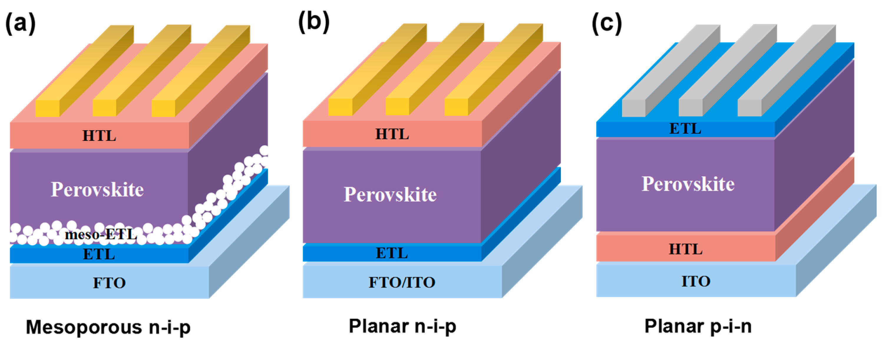
:1. Introduction
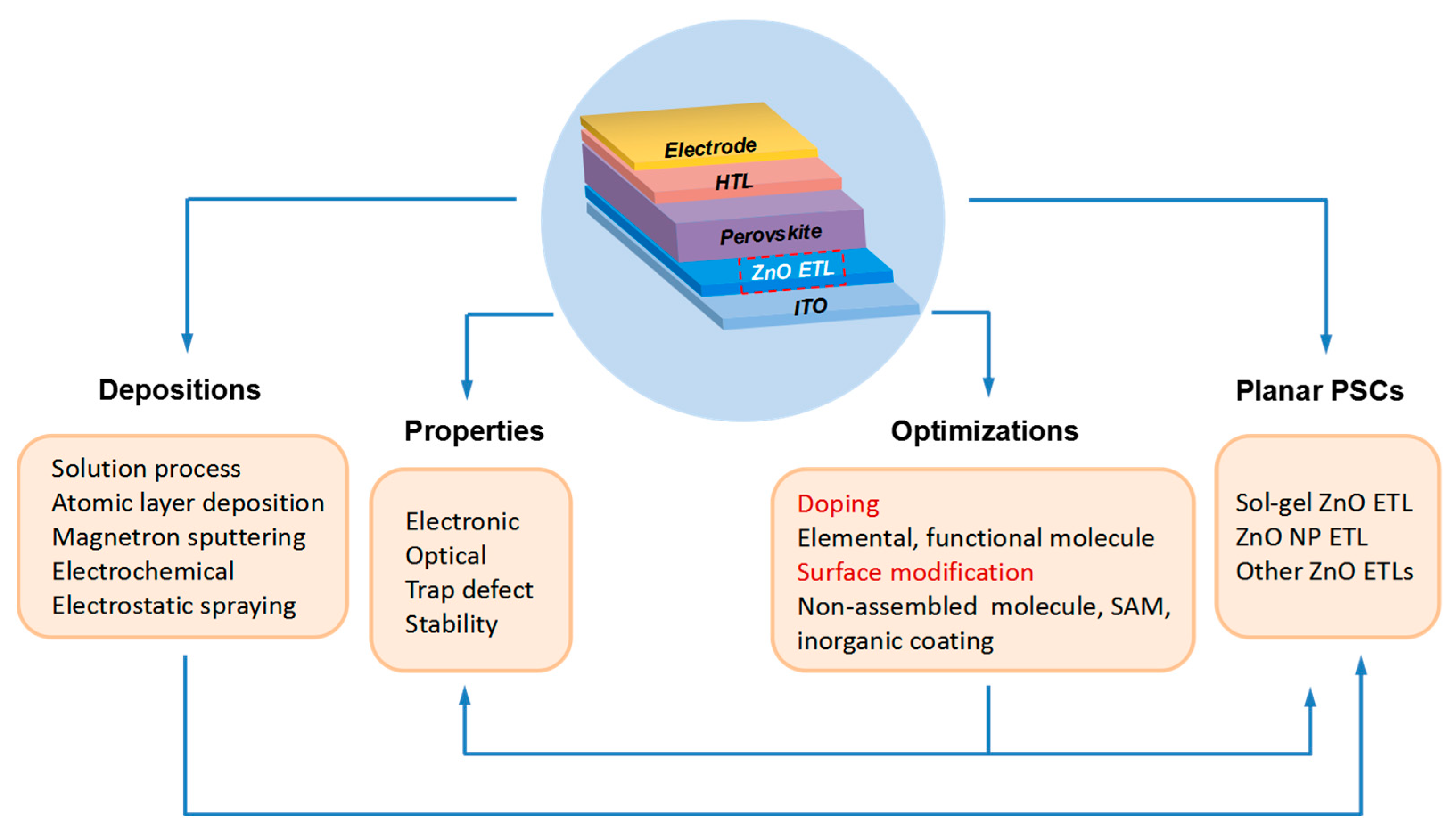
2. ZnO Electron Transport Layer
2.1. Basic Properties of ZnO
2.1.1. Optoelectronic Property
2.1.2. Defects
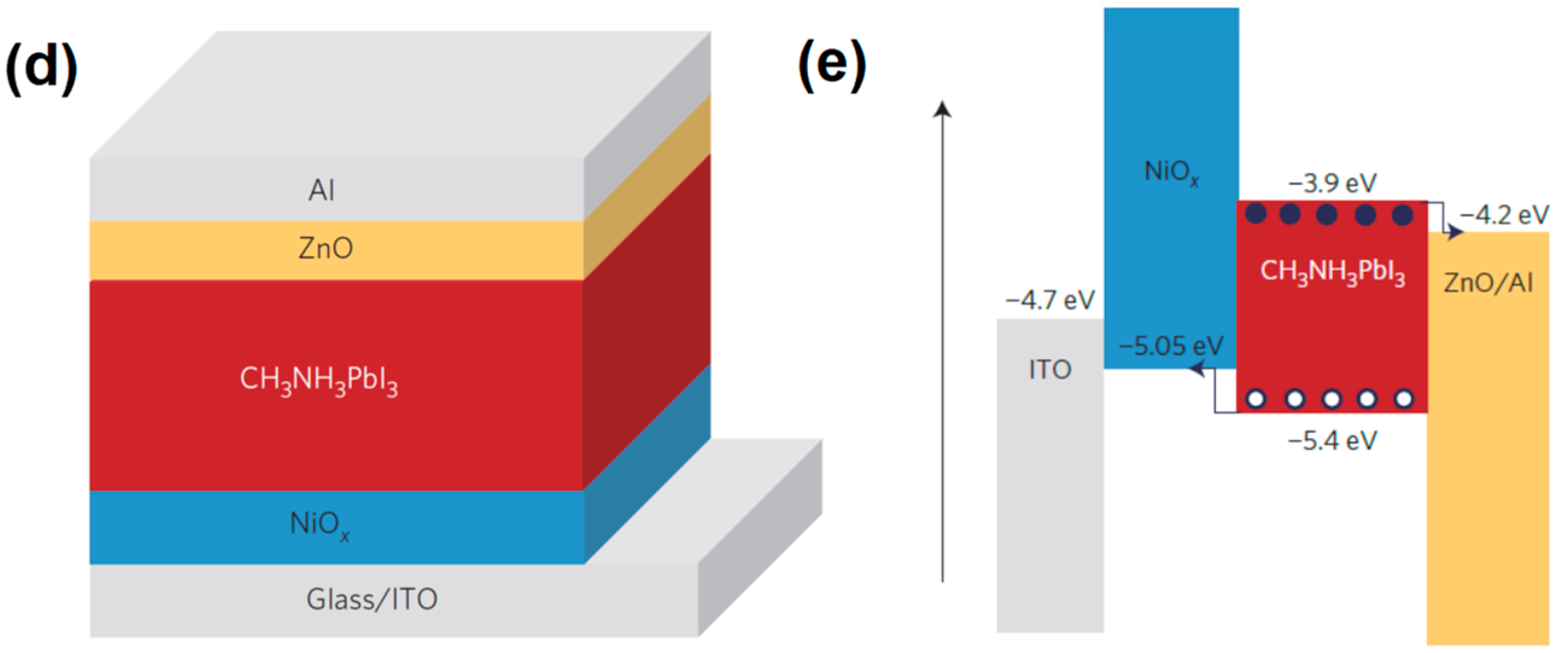
2.1.3. Stability
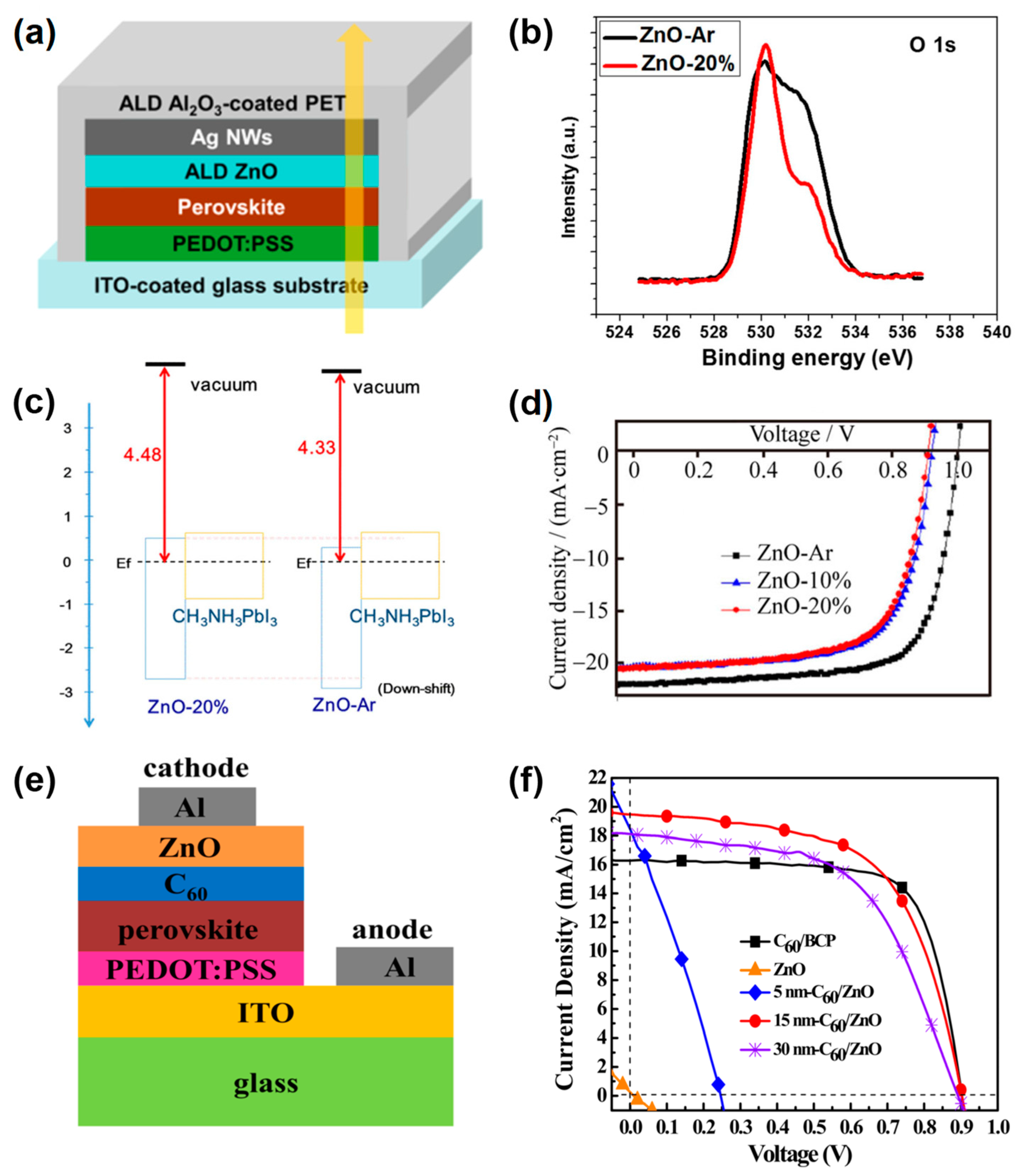
2.1.4. Regulation of Basic Properties
2.2. Deposition Methods of Compact ZnO ETL
2.2.1. Solution Process
2.2.2. Atomic Layer Deposition (ALD)
2.2.3. Magnetron Sputtering Deposition
2.2.4. Electrochemical Deposition (ED) and Electrostatic Spraying

3. Planar PSCs with ZnO ETL
3.1. PSCs Based on Sol-Gel ZnO ETL
3.2. PSCs Based on ZnO NP ETL
3.3. PSCs Based on Other ZnO ETLs


| Deposition Method | Device Structure | Voc (V) | Jsc (mAcm−2) | FF (%) | PCE (%) | Ref. | |
|---|---|---|---|---|---|---|---|
| Planar | Sol-gel | ITO/ZnO/MAPbI3/PTB7-Th/MoO3/Ag | 0.86 | 14.31 | 68 | 8.37 | [58] |
| Planar | Sol-gel | ITO/ZnO/MAPbI3/spiro-OMeTAD/Ag | 0.92 | 20.9 | 71 | 13.7 | [59] |
| Planar | Sol-gel | ITO/ZnO/CH3NH3PbI3−xClx/spiro-OMeTAD/Ag | 0.93 | 22.21 | 52.4 | 10.9 | [51] |
| Planar | Sol-gel | ITO/ZnO/MAPbI3/spiro-OMeTAD/Ag | 1.07 | 16.81 | 59 | 10.6 | [62] |
| Planar | Sol-gel | ITO/ZnO/(Cs0.1FA0.9PbI3)/spiro-OMeTAD/ Au | 1.08 | 24.67 | 74.49 | 19.84 | [63] |
| Planar | Nanoparticle | ITO/ZnO/MAPbI3/spiro-OMeTAD/Ag | 1.03 | 20.4 | 74.9 | 15.7 | [30] |
| Planar | Nanoparticle | PET/ITO/ZnO/MAPbI3/spiro-OMeTAD/Ag | 1.03 | 13.4 | 73.9 | 10.2 | [30] |
| Planar | Nanoparticle | ITO/ZnO/MAPbI3/P3HT/Ag | 0.98 | 20.38 | 59.9 | 11.96 | [65] |
| Planar | Nanoparticle | ZnO/MAPbI3/C | 0.54 | 19.98 | 54 | 8.73 | [66] |
| Planar | Nanoparticle | ITO/ZnO/FAPbI3/spiro-OMeTAD/Ag | 1.08 | 20.9 | 71.3 | 16.1 | [67] |
| Planar | Nanoparticle | ITO/ZnO/Cs6(MA0.17FA0.83)94Pb(I0.83Br0.17)3/ spiro-OMeTAD/Ag | 1.11 | 22.6 | 75.3 | 18.9 | [68] |
| Planar | Nanoparticle | FTO/ZnO/MAPbI3/spiro-OMeTAD/Au | 1.038 | 19.31 | 71.09 | 14.25 | [69] |
| Planar | Nanoparticle | ITO/ZnO/MAPbI3/P3HT/Ag | 0.949 | 18.8 | 66.1 | 11.8 | [64] |
| Inverted Planar | Nanoparticle | ITO/PEDOT:PSS/MAPbI3−xClx/PCBM/ ZnO/Al | 0.97 | 20.5 | 80.1 | 15.9 | [70] |
| Inverted Planar | Nanoparticle | ITO/PEDOT:PSS/MAPbIxCl3−x/PCBM/ ZnO/Al | 0.98 | 19.6 | 74.2 | 14.2 | [71] |
| Inverted Planar | Nanoparticle | ITO/NiOx/MAPbI3/ZnO/Al | 1.01 | 21.0 | 76.0 | 16.1 | [72] |
| Planar | ALD | ITO/ZnO/MAPbI3/spiro-OMeTAD/MoO3/Ag | 0.97 a | 14.15 a | 48 a | 6.59 a | [73] |
| Planar | ALD | FTO/ZnO/MAPbI3/spiro-OMeTAD/Ag | 0.97 | 20.40 | 66.00 | 13.10 | [74] |
| Inverted Planar | ALD | ITO/PEDOT:PSS/MAPbI3/ZnO/Ag | 1.03 | 20.75 | 77.03 | 16.5 | [32] |
| Planar | Magnetron sputtering | ITO/ZnO/MAPbI3/spiro-OMeTAD/MoO3/Ag | 1.04 | 22.4 | 57.4 | 13.4 | [75] |
| Planar | Magnetron sputtering | PET/ITO/ZnO/MAPbI3/spiro-OMeTAD/ MoO3/Ag | 0.87 | 18.4 | 49.7 | 8.03 | [75] |
| Planar | Magnetron sputtering | ITO/ZnO/MAPbI3/spiro-OMeTAD/Ag | 1.00 | 21.8 | 72.6 | 15.9 | [33] |
| Inverted Planar | Magnetron sputtering | ITO/PEDOT:PSS/MAPbI3/C60/ZnO/Al | 0.91 | 19.41 | 62.0 | 10.93 | [76] |
| Planar | ED | FTO/ZnO/MAPbI3/spiro-OMeTAD/Au | 1.02 | 16.98 | 51.11 | 8.90 | [29] |
| Planar | ED | FTO/ZnO/MAPbI3/spiro-OMeTAD/Ag | 1.08 | 20.04 | 69.47 | 14.99 | [59] |
| Planar | Electrostatic spraying | FTO/ZnO/MAPbI3/spiro-OMeTAD/Ag | 1.01 a | 16.0 a | 67.0 a | 10.8 a | [27] |
4. The Optimization of ZnO ETLs for Efficient Planar PSCs
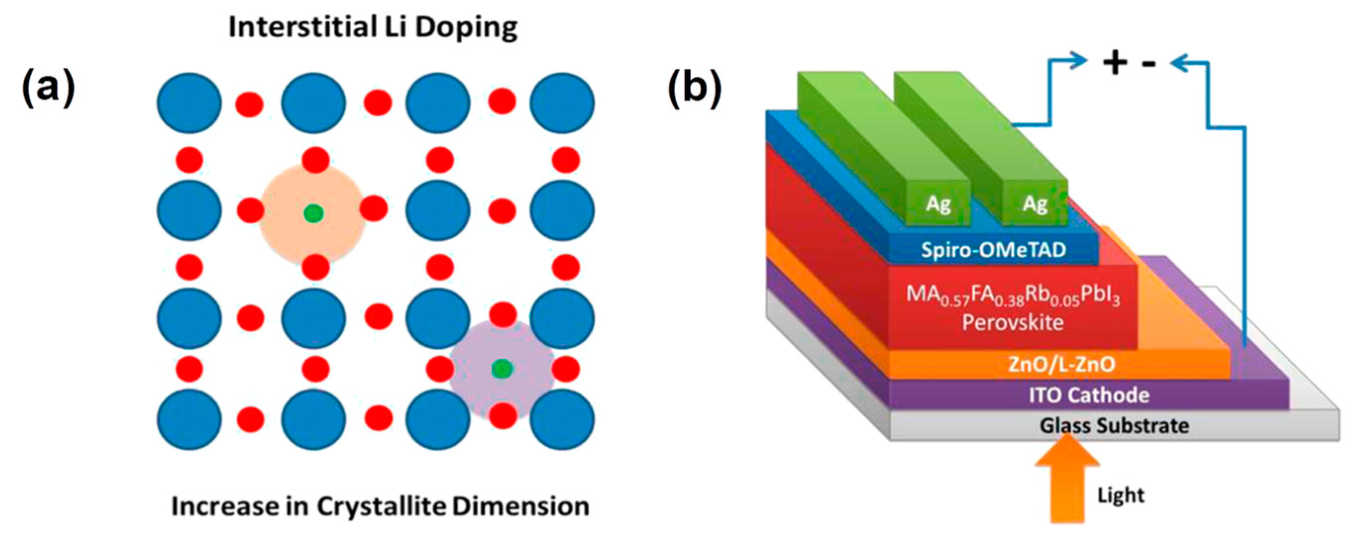
4.1. Doping of ZnO ETL


4.2. Surface Modification of ZnO ETL

5. Conclusions and Prospective
Author Contributions
Funding
Institutional Review Board Statement
Informed Consent Statement
Data Availability Statement
Conflicts of Interest
References
- O’regan, B.; Grätzel, M. A low-cost, high-efficiency solar cell based on dye-sensitized colloidal TiO2 films. Nature 1991, 353, 737–740. [Google Scholar] [CrossRef]
- Gur, I.; Fromer, N.A.; Geier, M.L.; Alivisatos, A.P. Air-stable all-inorganic nanocrystal solar cells processed from solution. Science 2005, 310, 462–465. [Google Scholar] [CrossRef] [Green Version]
- Zeng, G.; Zhang, J.; Chen, X.; Gu, H.; Li, Y.; Li, Y. Breaking 12% efficiency in flexible organic solar cells by using a composite electrode. Sci. China Chem. 2019, 62, 851–858. [Google Scholar] [CrossRef]
- Zhou, Y.; Li, X.; Lin, H. To be higher and stronger-metal oxide electron transport materials for perovskite solar cells. Small 2020, 16, 1902579. [Google Scholar] [CrossRef]
- Ouyang, D.; Huang, Z.; Choy, W.C. Solution-processed metal oxide nanocrystals as carrier transport layers in organic and perovskite solar cells. Adv. Funct. Mater. 2019, 29, 1804660. [Google Scholar] [CrossRef] [Green Version]
- Kojima, A.; Teshima, K.; Shirai, Y.; Miyasaka, T. Organometal halide perovskites as visible-light sensitizers for photovoltaic cells. J. Am. Chem. Soc. 2009, 131, 6050–6051. [Google Scholar] [CrossRef]
- Jeon, N.J.; Noh, J.H.; Kim, Y.C.; Yang, W.S.; Ryu, S.; Seok, S.I. Solvent engineering for high-performance inorganic–organic hybrid perovskite solar cells. Nat. Mater. 2014, 13, 897–903. [Google Scholar] [CrossRef]
- Zhang, M.; Chen, Q.; Xue, R.; Zhan, Y.; Wang, C.; Lai, J.; Yang, J.; Lin, H.; Yao, J.; Li, Y.; et al. Reconfiguration of interfacial energy band structure for high-performance inverted structure perovskite solar cells. Nat. Commun. 2019, 10, 4593. [Google Scholar] [CrossRef] [Green Version]
- Jiang, Q.; Ni, Z.; Xu, G.; Lin, Y.; Rudd, P.N.; Xue, R.; Li, Y.; Li, Y.; Gao, Y.; Huang, J. Interfacial molecular doping of metal halide perovskites for highly efficient solar cells. Adv. Mater. 2020, 32, 2001581. [Google Scholar] [CrossRef]
- National Renewable Energy Laboratory 2022, Best Research Cell Efficiencies. Available online: https://www.nrel.gov/pv/assets/pdfs/best-research-cell-efficiencies.pdf. (accessed on 30 September 2022).
- Im, J.H.; Lee, C.R.; Lee, J.W.; Park, S.W.; Park, N.G. 6.5% efficient perovskite quantum-dot-sensitized solar cell. Nanoscale 2011, 3, 4088–4093. [Google Scholar] [CrossRef]
- Kim, H.S.; Lee, C.R.; Im, J.H.; Lee, K.B.; Moehl, T.; Marchioro, A.; Moon, S.J.; Humphry-Baker, R.; Yum, J.H.; Moser, J.E.; et al. Lead iodide perovskite sensitized all-solid-state submicron thin film mesoscopic solar cell with efficiency exceeding 9%. Sci. Rep. 2012, 2, 591. [Google Scholar] [CrossRef] [Green Version]
- Burschka, J.; Pellet, N.; Moon, S.J.; Humphry-Baker, R.; Gao, P.; Nazeeruddin, M.K.; Grätzel, M. Sequential deposition as a route to high-performance perovskite-sensitized solar cells. Nature 2013, 499, 316–319. [Google Scholar] [CrossRef]
- Shaikh, S.F.; Kwon, H.C.; Yang, W.; Mane, R.S.; Moon, J. Performance enhancement of mesoporous TiO2-based perovskite solar cells by ZnS ultrathin-interfacial modification layer. J. Alloy. Compd. 2018, 738, 405–414. [Google Scholar] [CrossRef]
- Shin, S.S.; Lee, S.J.; Seok, S.I. Metal oxide charge transport layers for efficient and stable perovskite solar cells. Adv. Funct. Mater. 2019, 29, 1900455. [Google Scholar] [CrossRef]
- Song, J.X.; Yin, X.X.; Li, Z.F.; Li, Y.W. Low-temperature-processed metal oxide electron transport layers for efficient planar perovskite solar cells. Rare Met. 2021, 40, 2730–2746. [Google Scholar] [CrossRef]
- Stranks, S.D.; Eperon, G.E.; Grancini, G.; Menelaou, C.; Alcocer, M.J.P.; Leijtens, T.; Herz, L.M.; Petrozza, A.; Snaith, H.J. Electron-hole diffusion lengths exceeding 1 micrometer in an organometal trihalide perovskite absorber. Science 2013, 342, 341–344. [Google Scholar] [CrossRef] [Green Version]
- Liu, M.; Johnston, M.B.; Snaith, H.J. Efficient planar heterojunction perovskite solar cells by vapour deposition. Nature. 2013, 501, 395–398. [Google Scholar] [CrossRef]
- Docampo, P.; Ball, J.M.; Darwich, M.; Eperon, G.E.; Snaith, H.J. Efficient organometal trihalide perovskite planar-heterojunction solar cells on flexible polymer substrates. Nat. Commun. 2013, 4, 2761. [Google Scholar] [CrossRef] [Green Version]
- Zhou, H.; Chen, Q.; Li, G.; Luo, S.; Song, T.B.; Duan, H.S.; Hong, Z.; You, J.; Liu, Y.; Yang, Y. Interface engineering of highly efficient perovskite solar cells. Science 2014, 345, 542–546. [Google Scholar] [CrossRef]
- Song, J.; Zheng, E.; Bian, J.; Wang, X.F.; Tian, W.; Sanehira, Y.; Miyasaka, T. Low-temperature SnO2-based electron selective contact for efficient and stable perovskite solar cells. J. Mater. Chem. A 2015, 3, 10837–10844. [Google Scholar] [CrossRef]
- Ke, W.; Fang, G.; Liu, Q.; Xiong, L.; Qin, P.; Tao, H.; Wang, J.; Lei, H.; Li, B.; Wan, J.; et al. Low-temperature solution-processed tin oxide as an alternative electron transporting layer for efficient perovskite solar cells. J. Am. Chem. Soc. 2015, 137, 6730–6733. [Google Scholar] [CrossRef]
- Wang, Z.L. Zinc oxide nanostructures: Growth, properties and applications. J. Phys. Condens. Matter 2004, 16, R829. [Google Scholar] [CrossRef]
- Zhang, Q.; Dandeneau, C.S.; Zhou, X.; Cao, G. ZnO nanostructures for dye-sensitized solar cells. Adv. Mater. 2009, 21, 4087–4108. [Google Scholar] [CrossRef]
- Dong, J.; Zhao, Y.; Shi, J.; Wei, H.; Xiao, J.; Xu, X.; Luo, J.; Xu, J.; Li, D.; Luo, Y.; et al. Impressive enhancement in the cell performance of ZnO nanorod-based perovskite solar cells with Al-doped ZnO interfacial modification. Chem. Commun. 2014, 50, 13381–13384. [Google Scholar] [CrossRef]
- Zhang, J.; Barboux, P.; Pauporté, T. Electrochemical design of nanostructured ZnO charge carrier layers for efficient solid-state perovskite-sensitized solar cells. Adv. Energy Mater. 2014, 4, 1400932. [Google Scholar] [CrossRef]
- Mahmood, K.; Swain, B.S.; Jung, H.S. Controlling the surface nanostructure of ZnO and Al-doped ZnO thin films using electrostatic spraying for their application in 12% efficient perovskite solar cells. Nanoscale 2014, 6, 9127–9138. [Google Scholar] [CrossRef]
- Son, D.Y.; Im, J.H.; Kim, H.S.; Park, N.G. 11% efficient perovskite solar cell based on ZnO nanorods: An effective charge collection system. J. Phys. Chem. 2014, 118, 16567–16573. [Google Scholar] [CrossRef]
- Kumar, M.H.; Yantara, N.; Dharani, S.; Graetzel, M.; Mhaisalkar, S.; Boix, P.P.; Mathews, N. Flexible, low-temperature, solution processed ZnO-based perovskite solid state solar cells. Chem. Commun. 2013, 49, 11089–11091. [Google Scholar] [CrossRef]
- Liu, D.; Kelly, T.L. Perovskite solar cells with a planar heterojunction structure prepared using room-temperature solution processing techniques. Nat. Photonics 2014, 8, 133–138. [Google Scholar] [CrossRef]
- Zuo, L.; Gu, Z.; Ye, T.; Fu, W.; Wu, G.; Li, H.; Chen, H. Enhanced photovoltaic performance of CH3NH3PbI3 perovskite solar cells through interfacial engineering using self-assembling monolayer. J. Am. Chem. Soc. 2015, 137, 2674–2679. [Google Scholar] [CrossRef]
- Chang, C.Y.; Lee, K.T.; Huang, W.K.; Siao, H.Y.; Chang, Y.C. High-performance, air-stable, low-temperature processed semitransparent perovskite solar cells enabled by atomic layer deposition. Chem. Mater. 2015, 27, 5122–5130. [Google Scholar] [CrossRef]
- Tseng, Z.L.; Chiang, C.H.; Wu, C.G. Surface engineering of ZnO thin film for high efficiency planar perovskite solar cells. Sci. Rep. 2015, 5, 13211. [Google Scholar] [CrossRef] [Green Version]
- Zhang, P.; Wu, J.; Zhang, T.; Wang, Y.; Liu, D.; Chen, H.; Ji, L.; Liu, C.; Ahmad, W.; Chen, Z.D.; et al. Perovskite solar cells with ZnO electron-transporting materials. Adv. Mater. 2018, 30, 1703737. [Google Scholar] [CrossRef]
- Cao, J.; Wu, B.; Chen, R.; Wu, Y.; Hui, Y.; Mao, B.W.; Zheng, N. Efficient, Hysteresis-Free, and Stable Perovskite Solar Cells with ZnO as Electron-Transport Layer: Effect of Surface Passivation. Adv. Mater. 2018, 30, 1705596. [Google Scholar] [CrossRef]
- Schutt, K.; Nayak, P.K.; Ramadan, A.J.; Wenger, B.; Lin, Y.H.; Snaith, H.J. Overcoming zinc oxide interface instability with a methylammonium-free perovskite for high-performance solar cells. Adv. Funct. Mater. 2019, 29, 1900466. [Google Scholar] [CrossRef]
- Singh, T.; Singh, J.; Miyasaka, T. Role of metal oxide electron-transport layer modification on the stability of high performing perovskite solar cells. ChemSusChem 2016, 9, 2559–2566. [Google Scholar] [CrossRef]
- Haque, M.A.; Sheikh, A.D.; Guan, X.; Wu, T. Metal oxides as efficient charge transporters in perovskite solar cells. Adv. Energy Mater. 2017, 7, 1602803. [Google Scholar] [CrossRef]
- Jiang, Q.; Zhang, X.; You, J. SnO2: A wonderful electron transport layer for perovskite solar cells. Small 2018, 14, 1801154. [Google Scholar] [CrossRef]
- Xue, S.W.; Zu, X.T.; Zhou, W.L.; Deng, H.X.; Xiang, X.; Zhang, L.; Deng, H. Effects of post-thermal annealing on the optical constants of ZnO thin film. J. Alloys Compd. 2008, 448, 21–26. [Google Scholar] [CrossRef]
- Srikant, V.; Clarke, D.R. On the optical band gap of zinc oxide. J. Appl. Phys. 1998, 83, 5447–5451. [Google Scholar] [CrossRef]
- Look, D.C.; Reynolds, D.C.; Sizelove, J.R.; Jones, R.L.; Litton, C.W.; Cantwell, G.; Harsch, W.C. Electrical properties of bulk ZnO. Solid State Commun. 1998, 105, 399–401. [Google Scholar] [CrossRef]
- Pacholski, C.; Kornowski, A.; Weller, H. Self-assembly of ZnO: From nanodots to nanorods. Angew. Chem. Int. Ed. 2002, 41, 1188–1191. [Google Scholar] [CrossRef]
- Wang, X.; Summers, C.J.; Wang, Z.L. Large-scale hexagonal-patterned growth of aligned ZnO nanorods for nano-optoelectronics and nanosensor arrays. Nano Lett. 2004, 4, 423–426. [Google Scholar] [CrossRef]
- Kong, Y.C.; Yu, D.P.; Zhang, B.; Fang, W.; Feng, S.Q. Ultraviolet-emitting ZnO nanowires synthesized by a physical vapor deposition approach. Appl. Phys. Lett. 2001, 78, 407–409. [Google Scholar] [CrossRef]
- Sun, Y.; Fuge, G.M.; Fox, N.A.; Riley, D.J.; Ashfold, M.N. Synthesis of aligned arrays of ultrathin ZnO nanotubes on a Si wafer coated with a thin ZnO film. Adv. Mater. 2005, 17, 2477–2481. [Google Scholar] [CrossRef]
- Ronning, C.; Gao, P.X.; Ding, Y.; Wang, Z.L.; Schwen, D. Manganese-doped ZnO nanobelts for spintronics. Appl. Phys. Lett. 2004, 84, 783–785. [Google Scholar] [CrossRef] [Green Version]
- Luo, J.; Wang, Y.; Zhang, Q. Progress in perovskite solar cells based on ZnO nanostructures. Sol. Energy 2018, 163, 289–306. [Google Scholar] [CrossRef]
- Oba, F.; Nishitani, S.R.; Isotani, S.; Adachi, H.; Tanaka, I. Energetics of native defects in ZnO. J. Appl. Phys. 2001, 90, 824–828. [Google Scholar] [CrossRef] [Green Version]
- Kohan, A.F.; Ceder, G.; Morgan, D.; Van de Walle, C.G. First-principles study of native point defects in ZnO. Phys. Rev. 2000, 61, 15019. [Google Scholar] [CrossRef] [Green Version]
- Yang, J.; Siempelkamp, B.D.; Mosconi, E.; De Angelis, F.; Kelly, T.L. Origin of the thermal instability in CH3NH3PbI3 thin films deposited on ZnO. Chem. Mater. 2015, 27, 4229–4236. [Google Scholar] [CrossRef]
- Zhang, P.; Wu, J.; Wang, Y.; Sarvari, H.; Liu, D.; Chen, Z.D.; Li, S. Enhanced efficiency and environmental stability of planar perovskite solar cells by suppressing photocatalytic decomposition. J. Mater. Chem. 2017, 5, 17368–17378. [Google Scholar] [CrossRef]
- Zhao, Y.H.; Zhang, K.C.; Wang, Z.W.; Huang, P.; Zhu, K.; Li, Z.D.; Li, D.H.; Yuan, L.G.; Zhou, Y.; Song, B. Comprehensive study of sol-gel versus hydrolysis-condensation methods to prepare ZnO films: Electron transport layers in perovskite solar cells. ACS Appl. Mater. Interfaces 2017, 9, 26234–26241. [Google Scholar] [CrossRef] [PubMed]
- Song, J.; Bian, J.; Zheng, E.; Wang, X.F.; Tian, W.; Miyasaka, T. Efficient and environmentally stable perovskite solar cells based on ZnO electron collection layer. Chem. Lett. 2015, 44, 610–612. [Google Scholar] [CrossRef] [Green Version]
- Sun, Y.; Seo, J.H.; Takacs, C.J.; Seifter, J.; Heeger, A.J. Inverted polymer solar cells integrated with a low-temperature-annealed sol-gel-derived ZnO film as an electron transport layer. Adv. Mater. 2011, 23, 1679–1683. [Google Scholar] [CrossRef]
- Oviroh, P.O.; Akbarzadeh, R.; Pan, D.; Coetzee, R.A.M.; Jen, T.C. New development of atomic layer deposition: Processes, methods and applications. Sci. Technol. Adv. Mater. 2019, 20, 465–496. [Google Scholar] [CrossRef] [PubMed] [Green Version]
- Carcia, P.F.; McLean, R.S.; Reilly, M.H.; Nunes, G., Jr. Transparent ZnO thin-film transistor fabricated by rf magnetron sputtering. Appl. Phys. Lett. 2003, 82, 1117–1119. [Google Scholar] [CrossRef]
- Kim, K.H.; Park, K.C.; Ma, D.Y. Structural, electrical and optical properties of aluminum doped zinc oxide films prepared by radio frequency magnetron sputtering. J. Appl. Phys. 1997, 81, 7764–7772. [Google Scholar] [CrossRef]
- Zhang, J.; Pauporté, T. Effects of oxide contact layer on the preparation and properties of CH3NH3PbI3 for perovskite solar cell application. J. Phys. Chem. 2015, 119, 14919–14928. [Google Scholar] [CrossRef]
- Kim, J.; Kim, G.; Kim, T.K.; Kwon, S.; Back, H.; Lee, J.; Lee, H.S.; Kang, H.; Lee, K. Efficient planar-heterojunction perovskite solar cells achieved via interfacial modification of a sol-gel ZnO electron collection layer. J. Mater. Chem. A 2014, 2, 17291–17296. [Google Scholar] [CrossRef]
- Manspeaker, C.; Scruggs, P.; Preiss, J.; Lyashenko, D.A.; Zakhidov, A.A. Reliable annealing of CH3NH3PbI3 films deposited on ZnO. J. Phys. Chem. 2016, 120, 6377–6382. [Google Scholar] [CrossRef]
- Zhou, J.; Meng, X.; Zhang, X.; Tao, X.; Zhang, Z.; Hu, J.; Wang, C.; Li, Y.; Yang, S. Low-temperature aqueous solution processed ZnO as an electron transporting layer for efficient perovskite solar cells. Mater. Chem. Front. 2017, 1, 802–806. [Google Scholar] [CrossRef]
- Zheng, D.; Wang, G.; Huang, W.; Wang, B.; Ke, W.; Logsdon, J.L.; Wang, H.; Wang, Z.; Zhu, W.; Yu, J.; et al. Combustion synthesized zinc oxide electron-transport layers for efficient and stable perovskite solar cells. Adv. Funct. Mater. 2019, 29, 1900265. [Google Scholar] [CrossRef]
- Liu, D.; Gangishetty, M.K.; Kelly, T.L. Effect of CH3NH3PbI3 thickness on device efficiency in planar heterojunction perovskite solar cells. J. Mater. Chem. 2014, 2, 19873–19881. [Google Scholar] [CrossRef] [Green Version]
- Hwang, K.; Jung, Y.S.; Heo, Y.J.; Scholes, F.H.; Watkins, S.E.; Subbiah, J.; Jones, D.J.; Kim, D.Y.; Vak, D. Toward large scale roll-to-roll production of fully printed perovskite solar cells. Adv. Mater. 2015, 27, 1241–1247. [Google Scholar] [CrossRef]
- Zhou, H.; Shi, Y.; Wang, K.; Dong, Q.; Bai, X.; Xing, Y.; Du, Y.; Ma, T. Low-temperature processed and carbon-based ZnO/CH3NH3PbI3/C planar heterojunction perovskite solar cells. J. Phys. Chem. 2015, 119, 4600–4605. [Google Scholar] [CrossRef]
- Song, J.; Hu, W.; Wang, X.F.; Chen, G.; Tian, W.; Miyasaka, T. HC(NH2)2PbI3 as a thermally stable absorber for efficient ZnO-based perovskite solar cells. J. Mater. Chem. 2016, 4, 8435–8443. [Google Scholar] [CrossRef]
- Song, J.; Liu, L.; Wang, X.F.; Chen, G.; Tian, W.; Miyasaka, T. Highly efficient and stable low-temperature processed ZnO solar cells with triple cation perovskite absorber. J. Mater. Chem. 2017, 5, 13439–13447. [Google Scholar] [CrossRef]
- Guo, Y.; Kang, L.; Zhu, M.; Zhang, Y.; Li, X.; Xu, P. A strategy toward air-stable and high-performance ZnO-based perovskite solar cells fabricated under ambient conditions. Chem. Eng. J. 2018, 336, 732–740. [Google Scholar] [CrossRef]
- Bai, S.; Wu, Z.; Wu, X.; Jin, Y.; Zhao, N.; Chen, Z.; Mei, Q.; Wang, X.; Ye, Z.; Song, T.; et al. High-performance planar heterojunction perovskite solar cells: Preserving long charge carrier diffusion lengths and interfacial engineering. Nano Res. 2014, 7, 1749–1758. [Google Scholar] [CrossRef]
- Qiu, W.; Buffiere, M.; Brammertz, G.; Paetzold, U.W.; Froyen, L.; Heremans, P.; Cheyns, D. High efficiency perovskite solar cells using a PCBM/ZnO double electron transport layer and a short air-aging step. Org. Electron. 2015, 26, 30–35. [Google Scholar] [CrossRef]
- You, J.; Meng, L.; Song, T.B.; Guo, T.F.; Yang, Y.M.; Chang, W.H.; Hong, Z.; Chen, H.; Zhou, H.; Chen, Q.; et al. Improved air stability of perovskite solar cells via solution-processed metal oxide transport layers. Nat. Nanotechnol. 2016, 11, 75–81. [Google Scholar] [CrossRef]
- Lee, K.M.; Chang, S.H.; Wang, K.H.; Chang, C.M.; Cheng, H.M.; Kei, C.C.; Tseng, Z.L.; Wu, C.G. Thickness effects of ZnO thin film on the performance of tri-iodide perovskite absorber based photovoltaics. Sol. Energy 2015, 120, 117–122. [Google Scholar] [CrossRef]
- Dong, X.; Hu, H.; Lin, B.; Ding, J.; Yuan, N. The effect of ALD-ZnO layers on the formation of CH3NH3PbI3 with different perovskite precursors and sintering temperatures. Chem. Commun. 2014, 50, 14405–14408. [Google Scholar] [CrossRef] [PubMed]
- Liang, L.; Huang, Z.; Cai, L.; Chen, W.; Wang, B.; Chen, K.; Bai, H.; Tian, Q.; Fan, B. Magnetron sputtered zinc oxide nanorods as thickness-insensitive cathode interlayer for perovskite planar-heterojunction solar cells. ACS Appl. Mater. Interfaces 2014, 6, 20585–20589. [Google Scholar] [CrossRef]
- Lai, W.C.; Lin, K.W.; Guo, T.F.; Chen, P.; Wang, Y.T. Conversion efficiency improvement of inverted CH3NH3PbI3 perovskite solar cells with room temperature sputtered ZnO by adding the C60 interlayer. Appl. Phys. Lett. 2015, 107, 253301. [Google Scholar] [CrossRef] [Green Version]
- Tseng, Z.L.; Chiang, C.H.; Chang, S.H.; Wu, C.G. Surface engineering of ZnO electron transporting layer via Al doping for high efficiency planar perovskite solar cells. Nano Energy 2016, 28, 311–318. [Google Scholar] [CrossRef]
- Song, J.; Zheng, E.; Liu, L.; Wang, X.F.; Chen, G.; Tian, W.; Miyasaka, T. Magnesium-doped Zinc Oxide as Electron Selective Contact Layers for Efficient Perovskite Solar Cells. ChemSusChem 2016, 9, 2640–2647. [Google Scholar] [CrossRef]
- Mahmud, M.A.; Elumalai, N.K.; Upama, M.B.; Wang, D.; Soufiani, A.M.; Wright, M.; Xu, C.; Haque, F.; Uddin, A. Solution-Processed Lithium-Doped ZnO Electron Transport Layer for Efficient Triple Cation (Rb, MA, FA) Perovskite Solar Cells. ACS Appl. Mater. Interfaces 2017, 9, 33841–33854. [Google Scholar] [CrossRef]
- Azmi, R.; Hwang, S.; Yin, W.; Kim, T.W.; Ahn, T.K.; Jang, S.Y. High efficiency low-temperature processed perovskite solar cells integrated with alkali metal doped ZnO electron transport layers. ACS Energy Lett. 2018, 3, 1241–1246. [Google Scholar] [CrossRef]
- An, Q.; Fassl, P.; Hofstetter, Y.J.; Becker-Koch, D.; Bausch, A.; Hopkinson, P.E.; Vaynzof, Y. High performance planar perovskite solar cells by ZnO electron transport layer engineering. Nano Energy 2017, 39, 400–408. [Google Scholar] [CrossRef]
- Qin, F.; Meng, W.; Fan, J.; Ge, C.; Luo, B.; Ge, R.; Hu, L.; Jiang, F.; Liu, T.; Jiang, Y.; et al. Enhanced Thermochemical Stability of CH3NH3PbI3 Perovskite Films on Zinc Oxides via New Precursors and Surface Engineering. ACS Appl. Mater. Interfaces 2017, 9, 26045–26051. [Google Scholar] [CrossRef] [PubMed]
- Wang, Z.; Zhu, X.; Feng, J.; Wang, C.; Zhang, C.; Ren, X.; Priya, S.; Liu, S.F.; Yang, D. Antisolvent- and Annealing-Free Deposition for Highly Stable Efficient Perovskite Solar Cells via Modified ZnO. Adv. Sci. 2021, 8, 2002860. [Google Scholar] [CrossRef] [PubMed]
- Cheng, Y.; Yang, Q.D.; Xiao, J.; Xue, Q.; Li, H.W.; Guan, Z.; Yip, H.L.; Tsang, S.W. Decomposition of Organometal Halide Perovskite Films on Zinc Oxide Nanoparticles. ACS Appl. Mater. Interfaces 2015, 7, 19986–19993. [Google Scholar] [CrossRef] [PubMed]
- Liu, C.; Wu, W.; Zhang, D.; Li, Z.; Ren, G.; Han, W.; Guo, W. Effective stability enhancement in ZnO-based perovskite solar cells by MACl modification. J. Mater. Chem. 2021, 9, 12161–12168. [Google Scholar] [CrossRef]
- Azmi, R.; Lee, C.L.; Jung, I.H.; Jang, S.Y. Simultaneous Improvement in Efficiency and Stability of Low-Temperature-Processed Perovskite Solar Cells by Interfacial Control. Adv. Energy Mater. 2018, 8, 1702934. [Google Scholar] [CrossRef]
- Azmi, R.; Hadmojo, W.T.; Sinaga, S.; Lee, C.L.; Yoon, S.C.; Jung, I.H.; Jang, S.Y. High-Efficiency Low-Temperature ZnO Based Perovskite Solar Cells Based on Highly Polar, Nonwetting Self-Assembled Molecular Layers. Adv. Energy Mater. 2018, 8, 1701683. [Google Scholar] [CrossRef]
- Wu, Y.; Song, J.; Wu, X.; Qiu, C.; Yin, X.; Hu, L.; Su, Z.; Jin, Y.; Chen, J.; Li, Z. Highly efficient and stable ZnO-based perovskite solar cells enabled by a self-assembled monolayer as the interface linker. Chem. Commun. 2022, 58, 9266–9269. [Google Scholar] [CrossRef]
- Chen, R.; Cao, J.; Duan, Y.; Hui, Y.; Chuong, T.T.; Ou, D.; Han, F.; Cheng, F.; Huang, X.; Wu, B.; et al. High-Efficiency, Hysteresis-Less, UV-Stable Perovskite Solar Cells with Cascade ZnO-ZnS Electron Transport Layer. J. Am. Chem. Soc. 2019, 141, 541–547. [Google Scholar] [CrossRef]
- Pang, Z.; Yang, S.; Sun, Y.; He, L.; Wang, F.; Fan, L.; Chi, S.; Sun, X.; Yang, L.; Yang, J. Hydrophobic PbS QDs layer decorated ZnO electron transport layer to boost photovoltaic performance of perovskite solar cells. Chem. Eng. J. 2022, 439, 135701. [Google Scholar] [CrossRef]
- Tavakoli, M.M.; Tavakoli, R.; Yadav, P.; Kong, J. A graphene/ZnO electron transfer layer together with perovskite passivation enables highly efficient and stable perovskite solar cells. J. Mater. Chem. 2019, 7, 679–686. [Google Scholar] [CrossRef]


Publisher’s Note: MDPI stays neutral with regard to jurisdictional claims in published maps and institutional affiliations. |
© 2022 by the authors. Licensee MDPI, Basel, Switzerland. This article is an open access article distributed under the terms and conditions of the Creative Commons Attribution (CC BY) license (https://creativecommons.org/licenses/by/4.0/).
Share and Cite
Qiu, C.; Wu, Y.; Song, J.; Wang, W.; Li, Z. Efficient Planar Perovskite Solar Cells with ZnO Electron Transport Layer. Coatings 2022, 12, 1981. https://doi.org/10.3390/coatings12121981
Qiu C, Wu Y, Song J, Wang W, Li Z. Efficient Planar Perovskite Solar Cells with ZnO Electron Transport Layer. Coatings. 2022; 12(12):1981. https://doi.org/10.3390/coatings12121981
Chicago/Turabian StyleQiu, Chufeng, Yan Wu, Jiaxing Song, Wentao Wang, and Zaifang Li. 2022. "Efficient Planar Perovskite Solar Cells with ZnO Electron Transport Layer" Coatings 12, no. 12: 1981. https://doi.org/10.3390/coatings12121981