Communication

Phase Transition and Optical Properties of VO2 and Al: ZnO/VO2 Thin Films

1
Department of Physics, Deenbandhu Chhotu Ram University of Science and Technology, Murthal, Sonepat 131039, India
2
Pohang Accelerator Laboratory, POSTECH, Pohang 37673, Korea
*
Authors to whom correspondence should be addressed.
Coatings 2022, 12(11), 1737; https://doi.org/10.3390/coatings12111737
Submission received: 10 October 2022 / Revised: 10 November 2022 / Accepted: 11 November 2022 / Published: 13 November 2022
(This article belongs to the Special Issue Thin Films of Electronic Materials)

Abstract

:
Thermochromic Vanadium dioxide (VO2) has strong potential for smart window applications but its commercial scale usage is limited due to low visible light transmission. To address this issue, aluminum doped zinc oxide (AZO) anti-reflecting layer is integrated with VO2 layer in the present work. VO2 single layer and AZO/VO2 bilayer thin film samples were deposited by sputtering technique on quartz substrate. The single-phase growth of VO2 and AZO in single layer and bilayer thin film samples is confirmed by X-ray diffraction measurements. Monoclinic M1 phase of VO2 is detected in VO2 and AZO/VO2 thin film samples at room temperature. Monoclinic to rutile structural phase transition (SPT) in these samples is studied by performing temperature-dependent X-ray diffraction measurements. SPT in VO2 thin film samples is close to 68 °C and SPT temperature appears slightly lower in AZO/VO2 sample as compared to VO2 sample. Spectral transmittance measurement at room temperature showed significant improvement in the visible transmittance of AZO bilayer film than that of single layer VO2 thin film. These results demonstrate the possibility of integration of anti-reflecting layers such as AZO with VO2 layer for better visible transmittances suitable for large-scale smart window applications.

1. Introduction

The most common chromogenic materials are thermochromic, electrochromic, and photochromic materials which change their optical properties in response to temperature, external voltage bias, and photons, respectively. Thermochromic materials could potentially be used in wide technological applications such as Mott transistors, optical switches, filters, thermometers, smart windows, gas sensors, memory devices, and metamaterials [1,2,3,4,5,6,7]. Thermochromic materials involve temperature-dependent changes and are suitable for energy-saving smart windows to reduce building energy consumption [1,8,9]. Smart windows help to control the temperature inside the building even when there is a significant change in the temperature outside. Thermochromism can either be reversible or irreversible and can occur both over a range of temperatures or at particular transition temperature depending on the thermodynamics of the material [9]. Vanadium dioxide (VO2) is a popular thermochromic material which shows reversible insulation (monoclinic M1 crystal structure) to metal (rutile crystal structure) at a critical temperature of ~68 °C [8,10,11,12]. The structural and electrical phase transition is also accompanied by optical transition. Below 68 °C, monoclinic insulating phase of VO2 is infrared (IR) transparent while above 68 °C rutile metallic phase of VO2 is infrared (IR) opaque [1,12]. Compared to other thermochromic materials, the transition temperature of VO2 is closest to room temperature and therefore can be used for the development of smart windows [6,13]. This is the reason VO2 is explored as a thermochromic material for the smart windows application across the world. However, large-scale use of VO2 in smart window application is limited by its higher transition temperature and low visible transmittance. Therefore, different approaches such as deposition parameters control, strain/stress, doping, ion-implantation, oxygen vacancies, hydrogenation etc. [12,14,15,16,17,18] were extensively explored to tune the transition temperature of VO2 close to the room temperature. The other crucial issue of low visible transmittance in VO2 is not yet addressed well, unlike the issue of transition temperature tuning. Some groups have attempted to enhance the room temperature luminous transmittance of VO2 by means of integration of VO2 with an anti-reflecting layer such as TiO2, Ti:ZnO etc. [19,20,21,22]. In continuation, we have explored AZO (ZnO having 5 wt% Al) as an anti-reflecting layer for integration with VO2 in order to modify the luminous transmittance. ZnO is known to show good visible transmittance and its band gap can be tuned by properly selecting the dopant [23,24,25,26]. Earlier, attempts were made to study the effect of integration of AZO layer with VO2 [21,22]. However, these works lack structural phase transition study aspect in the integrated samples.
In present work, we have deposited VO2 single layer and AZO/VO2 bilayer thin film samples on quartz substrate by sputtering and studied their structural phase transition and optical properties. Higher luminous transmittance was observed in the AZO/VO2 sample compared to that of the VO2 sample, which highlights the importance of anti-reflecting layer for realization of VO2-based smart windows.

2. Materials and Methods
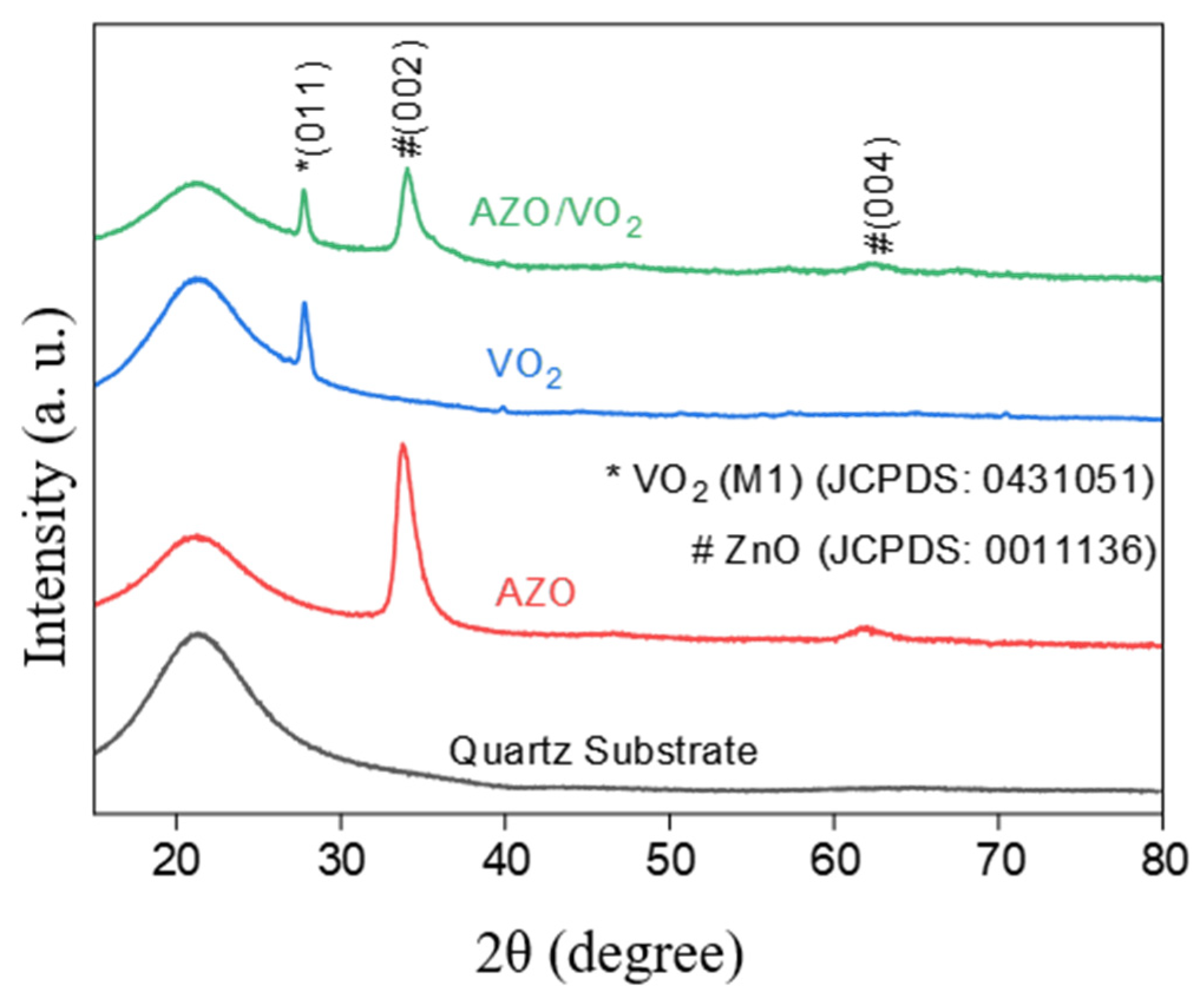
Ultrasonically cleaned quartz substrates were used to grow thin films of VO2 and AZO. Using radio frequency (RF) magnetron sputtering technique, VO2 and AZO layers were grown from commercially purchased VO2 and AZO targets, respectively. At first, VO2 thin film of about 100 nm thickness was simultaneously grown on two quartz substrates, one of which was used for bilayer growth later. Before the deposition, the deposition chamber was evacuated to 1 × 10⁻⁶ Torr. VO2 film growth was carried out at 500 °C temperature, 120 W deposition power and 30 mTorr sputtering Ar gas pressure. One of the VO2 thin film samples was taken out from the deposition chamber, and in place of it, another quartz substrate was mounted. Subsequently, AZO layer of about 50 nm thickness was simultaneously grown on substrate and the freshly prepared VO2 thin film sample. AZO layer growth was carried out at room temperature, 100 W deposition power and 35 mTorr sputtering Ar gas pressure. Table 1 tabulates the growth parameters for different layers of VO2 and AZO/VO2 thin film samples.
The crystallographic properties of the grown thin film samples were studied at BL5A beamline of Pohang Light source-II, Pohang, South Korea. Room temperature and temperature-dependent grazing incidence X-ray diffraction (GIXRD) measurements were performed with X-ray of 11.57 keV energy and the incidence angle was kept at 0.5°. The obtained GIXRD data was converted to Cu Kα wavelength using Bragg’s diffraction formula to show in the present work. The surface microstructure of films was characterised by field emission scanning electron microscopy (FESEM) using Sigma FESEM instrument (Zeiss Microsccopy, Jena, Germany). Furthermore, Lambda 950 UV-Vis spectrophotometer (Perkin Elmer, Waltham, MA, USA) in transmission mode was used to measure transmittance spectra in 200–800 nm wavelength range.

3. Results

Figure 1 shows the room temperature GIXRD data of grown samples along with substrate. In VO2 single layer thin film sample, apart from the substrate hump, only one diffraction peak is seen, and it belongs to (011) plane of monoclinic M1 phase of VO2 (JCPDS card number 0431051). This observation of single peak in the GIXRD data points to preferred growth of VO2 along this plane in single layer thin film sample. In case of AZO single layer sample, only the c-axis-oriented diffraction peaks representing the hexagonal structure of ZnO (JCPDS card number 0011136) are observed [27]. In AZO/VO2 bilayer thin film sample, the diffraction peaks observed in the GIXRD data are only those which appeared in the single layer VO2 and AZO thin film samples. Any other diffraction peak of significant intensity is not observed in the AZO/VO2 thin film sample. Room temperature GIXRD results confirm the single-phase growth of VO2 (monoclinic M1 phase) in single layer as well as bilayer sample. Moreover, the deposition of AZO layer on top of VO2 did not produce any significant changes in the crystalline structure of VO2. Earlier, extra peak corresponding to other vanadium oxides and/or zinc vanadate was observed when VO2 layer was grown on top of ZnO layer for substrate temperature higher than 250 °C [21].
After confirming the single-phase growth of VO2 in single and AZO/VO2 thin film samples, we have recorded the temperature-dependent GIXRD data of these samples focused to M(011) diffraction peak in temperature range 28 to 90 °C. This enabled us to track the structural phase transition in these samples. The temperature-dependent diffraction data of VO2 and AZO/VO2 thin film samples are shown in Figure 2a,b, respectively. In VO2 thin film sample, M(011) diffraction peak remains stable from 28 to ~60 °C, and beyond that it starts to shift towards lower 2θ values with increasing temperature and finally transforms to rutile phase R(110) diffraction peak. Similar behavior of M(011) diffraction peak with increasing temperature is also noticed in the AZO/VO2 thin film sample.
For better visualization of monoclinic to rutile structural phase transition and to identify the transition temperature in VO2 and AZO/VO2 thin film samples, the intensity variation of R(110) diffraction peak with increasing temperatures are plotted in Figure 3 for these samples. One can clearly see the emergence of R(110) diffraction peak when temperature is increased above 60 °C. The dotted line in Figure 3 represents the structural phase transition temperature (68 °C) seen in bulk VO2 and good quality thin film samples [10]. The temperature-dependent intensity variation of R(110) diffraction peak of VO2 thin film sample shown in Figure 3 also indicates that the structural phase transition temperature of this sample is close to 68 °C, which highlights its good growth quality. R(110) diffraction peak intensity variation trend is similar for VO2 as well as AZO/VO2 thin film samples, except the fact that the structural phase transition temperature in AZO/VO2 sample appears to be on slightly lower temperature than that of VO2 thin film sample. This is possible due to the formation of defects such as oxygen vacancies during the AZO layer growth on top of the VO2 thin film. As AZO layer was grown at room temperature and no further annealing was performed after that, the defects were fewer and the change in transition temperature of AZO/VO2 sample was not much different to that of VO2 layer.
The surface morphology of VO2 and AZO/VO2 thin film samples was studied by means of FESEM (as seen in Figure 4). From Figure 4a, it can be seen that VO2 film has large flat aggregated particles. In AZO/VO2 thin film sample, uniform and continuous grain growth of AZO on VO2 layer is observed (Figure 4b). Inset of Figure 4b shows the phot of VO2 and AZO/VO2 layers grown on quartz substrate. The uniform surface coverage of these layers is evident in this photo.
After structural characterization and surface morphological study of VO2 and AZO/VO2 thin film samples, UV-vis spectroscopy at room temperature in transmission mode was performed to examine the optical properties of these samples. Recorded UV-Vis spectra of VO2 and AZO/VO2 thin film samples in 200 to 800 nm range is shown in Figure 5. From Figure 5, it can be seen that growth of AZO layer on top of VO2 has significantly modulated the optical transmittance in AZO/VO2 sample as compared to the VO2 thin film sample. It is worthy to note that transmittance is very little for both films in the UV region, while transmittance in visible region is significantly higher for the AZO/VO2 bilayer film sample as compared to the VO2 single layer sample. Better transmittance of AZO/VO2 bilayer film sample is likely to be driven by the antireflection property of AZO layer that reduces the light loss by making use of phase change and the reflectivity dependence on index of refraction [19].

4. Conclusions

In summary, some initial results of VO2 single layer and AZO/VO2 bilayer films grown on quartz substrate by RF magnetron sputtering have been presented. Preferential crystal orientation of VO2 and AZO in single and bilayer samples was confirmed by GIXRD measurements at room temperature. GIXRD results confirmed the absence of any extra peak corresponding to other vanadium oxides and/or zinc vanadate in VO2 and azo/VO2 thin film samples. Temperature-dependent GIXRD measurements revealed the monoclinic to rutile structural phase transition in VO2 close to 68 °C and with slight shift towards lower temperature in AZO/VO2 thin film sample. Through UV-Vis spectroscopy, it was found that bilayer structures have significantly higher optical transmittance than the VO2 single layer, and the enhanced transmittance in bilayer sample is associated with anti-reflecting AZO layer. The use of anti-reflecting layer such as AZO leads to enhanced visible transmittance in the AZO/VO2 integrated structure and can eventually solve the issue of low visible transmittance of VO2 single layer.

Author Contributions

Data curation, C.S. and M.K; Methodology, C.S., P.S.R. and M.K.; writing—original draft preparation, C.S.; writing—review and editing, P.S.R. and M.K. All authors have read and agreed to the published version of the manuscript.

Funding

This work was supported by Council of Scientific Research (CSIR) and Frontiers in Science and Technology (FIST).

Institutional Review Board Statement

Not applicable.

Informed Consent Statement

Not applicable.

Data Availability Statement

The data that supports the findings of this study are available from the corresponding author upon reasonable request.

Acknowledgments

One of the authors, Chirag Saharan, is highly thankful to CSIR Delhi for providing research grants as JRF and SRF. Authors thanks Ravinder of IIT Guwahati for technical assistance.

Conflicts of Interest

The authors declare no conflict of interest.

References

  1. Zhou, J.; Gao, Y.; Zhang, Z.; Luo, H.; Cao, C.; Chen, Z.; Dai, L.; Liu, X. VO2 Thermochromic Smart Window for Energy Savings and Generation. Sci. Rep. 2013, 3, 1–5. [Google Scholar] [CrossRef] [Green Version]
  2. Liu, K.; Lee, S.; Yang, S.; Delaire, O.; Wu, J. Recent Progresses on Physics and Applications of Vanadium Dioxide. Mater. Today 2018, 21, 875–896. [Google Scholar] [CrossRef] [Green Version]
  3. Patel, A.; Pataniya, P.; Solanki, G.K.; Sumesh, C.K.; Patel, K.D.; Pathak, V.M. Fabrication, Photoresponse and Temperature Dependence of n-VO2/n-MoSe2 Heterojunction Diode. Superlattices Microstruct. 2019, 130, 160–167. [Google Scholar] [CrossRef]
  4. Lee, M.-J.; Park, Y.; Suh, D.-S.; Lee, E.-H.; Seo, S.; Kim, D.-C.; Jung, R.; Kang, B.-S.; Ahn, S.-E.; Lee, C.B.; et al. Two Series Oxide Resistors Applicable to High Speed and High Density Nonvolatile Memory. Adv. Mater. 2007, 19, 3919–3923. [Google Scholar] [CrossRef]
  5. Zheng, J.; Bao, S.; Jin, P. TiO2(R)/VO2(M)/TiO2(A) Multilayer Film as Smart Window: Combination of Energy-Saving, Antifogging and Self-Cleaning Functions. Nano Energy 2015, 11, 136–145. [Google Scholar] [CrossRef]
  6. Ocampo, O.; Antúnez, E.E.; Agarwal, V. Memristive Devices from Porous Silicon—ZnO/VO2 Nanocomposites. Superlattices Microstruct. 2015, 88, 198–203. [Google Scholar] [CrossRef]
  7. Li, W.; Yan, X.; Zhao, W. Preparation of Crystal Violet Lactone Complex and Its Effect on Discoloration of Metal Surface Coating. Polymers 2022, 14, 4443. [Google Scholar] [CrossRef]
  8. Cui, Y.; Ke, Y.; Liu, C.; Chen, Z.; Wang, N.; Zhang, L.; Zhou, Y.; Wang, S.; Gao, Y.; Long, Y. Thermochromic VO2 for Energy-Efficient Smart Windows. Joule 2018, 2, 1707–1746. [Google Scholar] [CrossRef] [Green Version]
  9. Wang, X.; Narayan, S. Thermochromic Materials for Smart Windows: A State-of-Art Review. Front. Energy Res. 2021, 9, 837. [Google Scholar] [CrossRef]
  10. Zylbersztejn, A.; Mott, N.F. Metal-Insulator Transition in Vanadium Dioxide. Phys. Rev. B 1975, 11, 4383–4395. [Google Scholar] [CrossRef]
  11. Kumar, M.; Singh, J.P.; Chae, K.H.; Park, J.; Lee, H.H. Annealing Effect on Phase Transition and Thermochromic Properties of VO2 Thin Films. Superlattices Microstruct. 2020, 137, 106335. [Google Scholar] [CrossRef]
  12. Kumar, M.; Rani, S.; Pal Singh, J.; Hwa Chae, K.; Kim, Y.; Park, J.; Hwi Lee, H. Structural Phase Control and Thermochromic Modulation of VO2 Thin Films by Post Thermal Annealing. Appl. Surf. Sci. 2020, 529, 147093. [Google Scholar] [CrossRef]
  13. Yang, Z.; Ko, C.; Ramanathan, S. Oxide Electronics Utilizing Ultrafast Metal-Insulator Transitions. Annu. Rev. Mater. Sci. 2011, 41, 337–367. [Google Scholar] [CrossRef]
  14. Mulchandani, K.; Soni, A.; Pathy, K.; Mavani, K.R. Structural Transformation and Tuning of Electronic Transitions by W-Doping in VO2 Thin Films. Superlattices Microstruct. 2021, 154, 106883. [Google Scholar] [CrossRef]
  15. Yang, J.; Li, D.; Wang, X.; Jin, H.; Li, J. Optimizing Phase Transition Temperature and Visible Transmittance of VO2 Films Driven by Synergistic Effect of La-Mo Co-Doping. Appl. Surf. Sci. 2022, 600, 154074. [Google Scholar] [CrossRef]
  16. Jeong, J.; Aetukuri, N.; Graf, T.; Schladt, T.D.; Samant, M.G.; Parkin, S.S.P. Suppression of Metal-Insulator Transition in VO2 by Electric Field-Induced Oxygen Vacancy Formation. Science 2013, 339, 1402–1405. [Google Scholar] [CrossRef] [PubMed]
  17. Mulchandani, K.; Soni, A.; Pathy, K.; Mavani, K.R. Rapid Hydrogenation of VO2 Thin Films via Metal-Acid Contact Method Using Mild Electric Fields at Room Temperature. Mater. Lett. 2021, 295, 129786. [Google Scholar] [CrossRef]
  18. Kumar, M.; Singh, S.; Lim, W.C.; Chae, K.H.; Lee, H.H. Effect of Implantation of Nitrogen Ions into VO2 Thin Films. Mater. Lett. 2022, 310, 131438. [Google Scholar] [CrossRef]
  19. Ji, Y.; Mattsson, A.; Niklasson, G.A.; Granqvist, C.G.; Österlund, L. Synergistic TiO2/VO2 Window Coating with Thermochromism, Enhanced Luminous Transmittance, and Photocatalytic Activity. Joule 2019, 3, 2457–2471. [Google Scholar] [CrossRef]
  20. Kumar, M.; Rani, S.; Lee, H.H. Effect of Ti:ZnO Layer on the Phase Transition and the Optical Properties of VO2 Film. J. Korean Phys. Soc. 2019, 75, 519–522. [Google Scholar] [CrossRef]
  21. Sato, K.; Hoshino, H.; Mian, M.S.; Okimura, K. Low-Temperature Growth of VO2 Films on Transparent ZnO/Glass and Al-Doped ZnO/Glass and Their Optical Transition Properties. Thin Solid Film. 2018, 651, 91–96. [Google Scholar] [CrossRef]
  22. Kang, L.; Gao, Y.; Luo, H.; Wang, J.; Zhu, B.; Zhang, Z.; Du, J.; Kanehira, M.; Zhang, Y. Thermochromic Properties and Low Emissivity of ZnO: Al/VO2 Double-Layered Films with a Lowered Phase Transition Temperature. Sol. Energy Mater. Sol. Cells 2011, 95, 3189–3194. [Google Scholar] [CrossRef]
  23. Devi, V.; Kumar, M.; Shukla, D.K.; Choudhary, R.J.; Phase, D.M.; Kumar, R.; Joshi, B.C. Structural, Optical and Electronic Structure Studies of Al Doped ZnO Thin Films. Superlattices Microstruct. 2015, 83, 431–438. [Google Scholar] [CrossRef]
  24. Devi, V.; Kumar, M.; Kumar, R.; Joshi, B.C. Effect of Substrate Temperature and Oxygen Partial Pressure on Structural and Optical Properties of Mg Doped ZnO Thin Films. Ceram. Int. 2015, 41, 6269–6273. [Google Scholar] [CrossRef]
  25. Devi, V.; Kumar, M.; Choudhary, R.J.; Phase, D.M.; Kumar, R.; Joshi, B.C. Band Offset Studies in Pulse Laser Deposited Zn1-XCdxO/ZnO Hetero-Junctions. J. Appl. Phys. 2015, 117, 225305. [Google Scholar] [CrossRef]
  26. Devi, V.; Kumar, M.; Kumar, R.; Singh, A.; Joshi, B.C. Band Offset Measurements in Zn1−x SbxO/ZnO Hetero-Junctions. J. Phys. D Appl. Phys. 2015, 48, 335103. [Google Scholar] [CrossRef]
  27. Kumar, M.; Singh, J.P.; Chae, K.H.; Kim, J.H.; Lee, H.H. Structure, Optical and Electronic Structure Studies of Ti:ZnO Thin Films. J. Alloys Compd. 2018, 759, 8–13. [Google Scholar] [CrossRef]
Figure 1. Room temperature GIXRD data of substrate, VO2, AZO and AZO/VO2 thin film samples.
Coatings 12 01737 g001
Figure 2. Temperature-dependent GIXRD data of (a) VO2 thin film sample and (b) AZO/VO2 thin film sample measured during heating cycle.
Coatings 12 01737 g002
Figure 3. Temperature-dependence intensity variation of R(110) diffraction peak (rutile phase of VO2) for VO2 and AZO/VO2 thin film samples.
Coatings 12 01737 g003
Figure 4. SEM images of (a) VO2 thin film sample and (b) AZO/VO2 thin film sample measured at room temperature. Inset of figure (b) shows the photo of sample used for SEM measurement.
Coatings 12 01737 g004
Figure 5. UV-Vis spectroscopy spectra of VO2 and AZO/VO2 thin film sample measured at room temperature.
Coatings 12 01737 g005
Table 1. Growth parameters for different layers of VO2 and AZO/VO2 thin film samples.
Film LayerTarget
RF (W)
Ar Gas
Pressure (mTorr)
Thickness
(nm)
VO212030100
AZO1003550
Publisher’s Note: MDPI stays neutral with regard to jurisdictional claims in published maps and institutional affiliations.

