Communication

Discontinuous Powder Aerosol Deposition: An Approach to Prepare Films Using Smallest Powder Quantities

1
Department of Functional Materials, University of Bayreuth, 95447 Bayreuth, Germany
2
Institute of Chemical Process Engineering, University of Stuttgart, 70174 Stuttgart, Germany
*
Author to whom correspondence should be addressed.
Coatings 2021, 11(7), 844; https://doi.org/10.3390/coatings11070844
Submission received: 10 June 2021 / Revised: 7 July 2021 / Accepted: 9 July 2021 / Published: 13 July 2021
(This article belongs to the Section Ceramic Coatings and Engineering Technology)

Abstract

:
This work shows that the powder aerosol deposition (PAD) method allows the formation of films in powder quantities of less than 60 mg, rather than the large amounts that are typically required for conventional powder aerosol deposition systems. This was achieved by changing the operation mode to a discontinuous one, resulting in operation times of several seconds. Semiconducting strontium titanate ferrate SrTi0.65Fe0.35O3−δ (STF35) was used as the powder to prove the equal behavior in terms of adhesion, film quality and electric conductivity compared to conventional powder-aerosol-deposited films.

1. Introduction

The powder aerosol deposition (PAD) method, also known as the aerosol deposition method (ADM) or vacuum kinetic spray process (VKS), has attracted increasing interest in industry and science over the last years [1,2,3,4]. This ceramic film deposition technique is carried out completely at room temperature. The raw ceramic particles are aerosolized by a gas flow and accelerated into a vacuum chamber by a pressure gradient. Typical working pressures for the PAD are 100 to 1000 mbar for the aerosol chamber and 0.01 to 10 mbar for the deposition chamber [5]. The impact of the particles with suitable kinetic energy leads to the formation of dense ceramic films on the substrate material. In addition, the particle size has to be suitable for the deposition process. While small particles (particle diameters less than 100 nm) are deflected by the bow shock in front of the substrate, particles with a diameter significantly larger than 10 µm lead to an abrasion of the substrate or of the previously deposited film. In return, non-agglomerated particles in the single-digit micrometer diameter range show good deposition behavior [1]. Neither substrate heating nor heating of the coating material is necessary [6]. The resulting films are fully dense and show good adherence. In addition to common technical oxide ceramics such as Al2O3 and TiO2, functional ceramics are increasing in importance [7]. The large variety of materials and the direct processing approach from raw powder makes PAD an interesting manufacturing process in the field of sensor technology [8,9]. The suitability of the PAD process for the fabrication of electrolytes in solid oxide fuel cells has already been demonstrated [10,11,12]. Furthermore, PAD can be used to process solid electrolytes such as Li7La3Zr2O12 (LLZO) for use in solid-state lithium batteries. The high ionic conductivity combined with the high deposition rates at room temperature makes this process interesting [13]. To date, many studies have addressed large-area deposition [14]; however, this requires large amounts of materials. Even when using a small deposition chamber, at least several grams of powder are required [15]. The deposition of very small powder quantities in the milligram range is of interest, especially when depositing new materials that are typically available only in lab-scale quantities.
In this study, we suggest a discontinuous process, which we refer to herein as discontinuous powder aerosol deposition (DPAD). The goal is to deposit powder quantities of less than 100 mg within short coating times of several seconds. The typical advantageous properties of PAD films should are also retained. Very recently, Shoji et al. used a discontinuous process to manufacture a battery cathode from a material combination of LiCoO2 and Li3BO3 [16]. Nevertheless, it has not yet been proven that DPAD films show identical behavior in terms of film quality, adhesion on the substrate and electric conductivity.

2. Materials and Methods

For this study, we used semiconducting strontium titanate ferrate SrTi0.65Fe0.35O3−δ (STF35) as the material to be deposited. STF35 is typically applied for resistive oxygen sensing applications [17]. It shows a high electrical conductivity in the temperature range between 300 and 700 °C and has already been processed using PAD [7,18]. The synthesis followed the mixed oxide route, with stoichiometrically mixed starting powders of SrCO3, TiO2 and Fe2O3. Milling these starting powders in a planetary ball mill (Fritsch Pulverisette 5, Idar-Oberstein, Germany) with cyclohexane as the solvent yielded uniformly mixed reactants, followed by a calcination at 1200 °C for 15 h in air atmosphere. Calcined powders were subsequently milled in cyclohexane to achieve a suitable particle size distribution for PAD, exhibiting a median diameter of d50 = 3.1 µm, as measured by laser diffraction (Malvern Mastersizer 2000, Worcestershire, United Kingdom). Excess solvent was removed using a Heidolph rotary evaporator and the powder was then stored at 200 °C in a drying oven.
In order to illustrate the difference between a conventional PAD apparatus and the proposed novel DPAD setup, Figure 1 describes the schematic layouts of both setups. In the conventional apparatus, as introduced in Figure 1a, a continuous carrier gas flow is forced through an aerosol generation chamber on a vibrating table, fluidizing the ceramic particles. A pressure gradient from the aerosol to the deposition chamber caused by the vacuum pump accelerates the particles through a nozzle and makes them collide with a substrate. If the velocity of the particles is suitable (typically above 150 m/s [19]), the collision leads to the formation of films, which is known as room-temperature impact consolidation (RTIC) [14].
The setup and operating mode of the proposed DPAD apparatus are shown in Figure 1b. This layout features several deviations from the standard setup, namely a miniaturized aerosol chamber, an additional gas pressure chamber, and a de Laval nozzle to achieve higher gas velocities. Here, a defined carrier gas volume and pressure are utilized to form and accelerate the aerosol instead of the continuous gas flow used in conventional PAD. Before each deposition run, oxygen as a carrier gas is fed through valve 1 into a gas pressure chamber with a total volume of 16,000 mm3 (including the piping between the valves and the gas pressure chamber). After closing valve 1, valve 2 is used to lower the pressure in the pressure chamber to the intended absolute pressure of 1.5 bar, controlled by the connected pressure gauge. The small powder quantities are filled into the aerosol chamber and subsequently a vacuum is slowly applied to the deposition chamber until an absolute pressure of below 1 mbar is reached. Since the aerosol and deposition chamber are directly connected by pipes, the STF35 powder is already at the identical vacuum level, whereas the pressure of 1.5 bar is held by the solenoid valve in the pressure chamber. When opening the solenoid valve (switching time of less than 3 milliseconds), a transient gas flow fluidizes and transports the STF35 powder through a round de Laval nozzle and ejects it onto the substrate within seconds. Within this short procedure, the film is formed and the coating is finished. Four different substrates are used to characterize the deposited films:
  • Fire-polished stainless steel substrates for film profile measurement with a laser scanning microscope (Zeiss LSM900, Oberkochen, Germany) and for the Daimler–Benz Rockwell-C adhesion tests [20,21];
  • Alumina substrates for scanning electron microscope (SEM, Zeiss Leo 1530, Oberkochen, Germany) fracture patterns;
  • Silicon wafer for X-ray diffraction analysis (XRD, Bruker D8 Advance, Billerica, MA, USA) measurements;
  • Alumina substrates with sputtered platinum interdigital electrodes for the temperature-dependent electrical conductivity measurements.
The weight difference of the aerosol chamber prior to and after the discontinuous deposition gives information about the actual powder mass that contributes to the film formation and the powder mass that remains in the aerosol chamber. In Table 1, the term “filled-in powders” means the mass prior to the discontinuous deposition process, whereas “discharged powders” denotes the mass that contributes to the film. Despite the significant reduction in powder quantities, the deposition efficiency (ratio between deposited film mass and discharged powder) remains in line with typical PAD value of about 0.1% [22]. The difference between the filled-in powder and the discharged powder sticks to the walls of the aerosol chamber and does not contribute to the film formation. The error of the balance is 1 mg. The different substrate materials and the related characterization methods are mentioned in Table 1.
A closer look at the formed film was taken using a confocal laser scanning microscope (Zeiss LSM900, Oberkochen, Germany) to assess the shapes of the films, while an SEM fracture pattern (Zeiss Leo 1530, Oberkochen, Germany) was used to assess the microstructures of the films. The crystalline phase composition, microstrain and the nanocrystalline structure were investigated using XRD (Bruker D8 ADVANCE, 1D-Lynxeye detector, Ge-Kα1 monochromator, Billerica, MA, USA), including Rietveld refinement (X’Pert HighScore Plus).
The adhesion of the film was proven via the Daimler–Benz Rockwell-C test in accordance with VDI 3198 [23]. Analogously to the Rockwell-C hardness measurement, a 120° diamond cone indenter was pressed into the film and the stainless steel substrate with a load of 150 kg (or 1471 N). Subsequently, an optical assessment of the indentation spot and its circumference was performed and it was categorized from HF1 (excellent adhesion, only minor cracks allowed) to HF6 (complete delamination of the surroundings of the indentation). According to VDI 3198 [23], the maximum film thickness may be less than or equal to 5 µm [20,21].
Electrical characterization was carried out at temperatures between 100 and 700 °C in 100 °C steps upon heating and cooling in air to investigate the typical PAD annealing behavior via temperature-dependent resistance measurements (DC, Keithley model 2700, Solon, OH, USA) of the film. Here, alumina with platinum sputtered interdigital electrodes was used as a substrate. The distance between the fingers d and the width of the fingers w of the electrodes were 10 µm, respectively. The length of the fingers l was 1 mm; therefore, the total surface area of the finger-structured electrodes was 0.8 mm × 1 mm, having n = 20 pairs of fingers. The film thickness h = 800 nm was derived using LSM. To obtain an approximately uniform film thickness on the electrode structure, the maximum of the Gaussian-distributed film contour (see Figure 2b and Figure 3, respectively) was aimed in the middle of the electrode structure. In the surroundings, with a radius of 0.5 mm around the maximum of the Gaussian-shaped contour, the film thickness can be assumed to be approximately constant. This allows the use of Equation (1) to calculate the geometry factor of the interdigital electrode and to determine the electrical conductivity σ from the measured electrical resistance R [24]:
σ = 1 R   d ( 2 n 1 ) l h + 2 n w h   = 1 R 3.1726 1 cm .

3. Results

The DPAD method will be discussed in the following sections, which allows the use of small powder quantities to obtain films of equal quality and behavior.

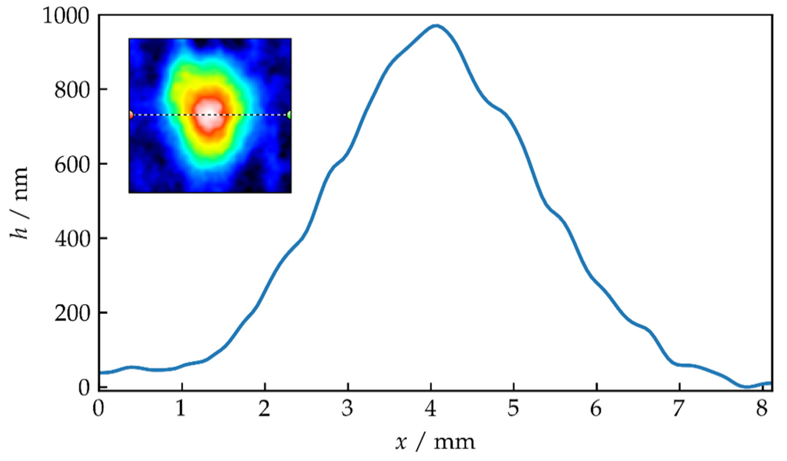
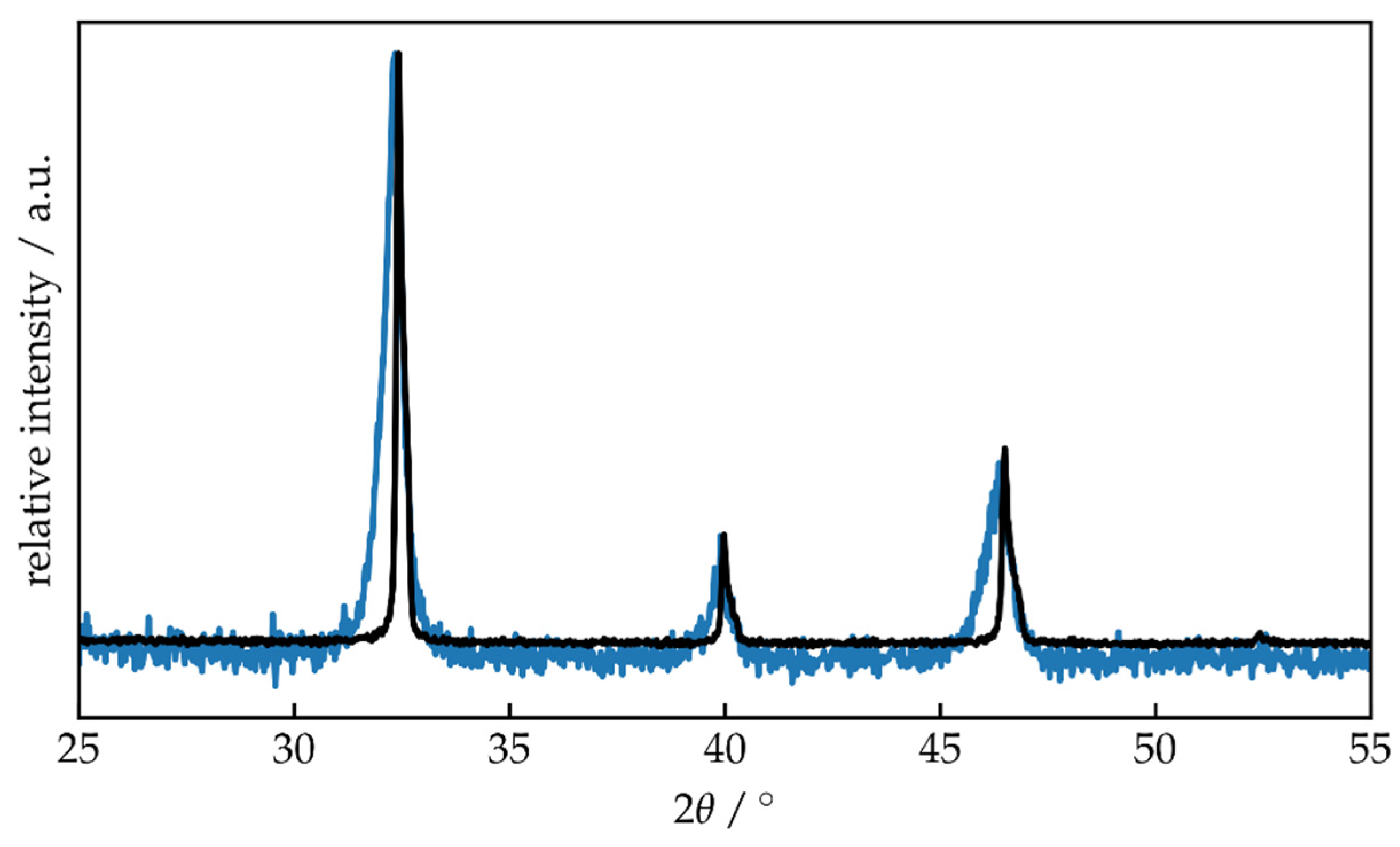
3.1. Contour, Thickness and Crystalline Structure of the Film

Figure 2a shows an STF35 film deposited on stainless steel. The circular contour of the film resulted from the round de Laval nozzle, with diameters of 1.6 and 5 mm for the throat and orifice, respectively. The darker appearance of the core zone relates to the throat diameter of the de Laval nozzle. The corresponding LSM image is shown in Figure 2b, where a Gaussian-shaped surface contour can be observed. The maximum film thickness of h ≈ 1 µm can be derived from the extracted two-dimensional profile in Figure 3. Similarly shaped profiles were observed for Al2O3, TiO2 and ZnO in another unpublished study.
An SEM fracture pattern of STF35 on an alumina substrate is shown in Figure 4. Starting from the synthesized STF35 powder with a mean particle diameter of 3.1 µm, the fracture pattern shows a dense film with crystallite fragments in the nanometer range. In accordance with Akedo et al., this is a typical feature of a PAD film, as the impact leads to fragmentation and distortion of the deposited particles [25].
An STF35 film deposited on silicon wafer was examined using XRD at 2θ-angles between 25° and 55°. Figure 5 shows the XRD pattern of the STF35 film and an STF powder reference. The positions of all reflexes coincide well, pointing out that a phase-pure STF film was formed by DPAD; however, a significant broadening of reflexes can be detected. These features are similar to conventional sprayed PAD films, as discussed by Sahner et al. [26]. The broadened reflexes are an indication of a strongly reduced crystallite size. An additional Rietveld refinement of the XRD pattern of the film yielded a crystallite size of 56 nm and a microstrain of 0.63%. The order of magnitude of the microstrain and the crystallite size fit very well to reported films of functional ceramics, such as BiCuTiVOx [27] and Li5.3Al0.4La3Zr1.5Ta0.5O12 (ALLZTO) [28].

3.2. Film Properties

The good adherence of the coatings is a key feature of PAD films; therefore, a Daimler–Benz Rockwell-C adhesion test was performed. The optical microscope image of the indentation is shown in Figure 6a. The image neither shows cracks nor any kind of delamination in the surroundings of the indentation and can, therefore, be classified as HF1 (excellent adhesion) according to the test chart in Figure 6b.
The electrical conductivity of STF35 films prepared by conventional PAD was carefully studied in [18]. As explained in [6], the electrical conductivity is already present within the as-deposited films, but is lowered by several orders of magnitude. To return the electrical conductivity to levels close to the bulk value, thermal post-treatment of the deposited film is often required. This annealing step restores the undistorted crystalline lattice, i.e., the microstrain diminishes [6,27,28].
An Arrhenius-like plot of the electric conductivity is shown in Figure 7. Starting at 100 °C and σ = 10−7 Scm−1, increasing the temperature T results in significantly increased conductivity, reaching a maximum of 4.6 × 10⁻³ Scm−1 at 700 °C. Upon first cooling, the conductivity decreases, with similar behavior to that described by [6], to approximately 10−5 Scm−1 at 100 °C. The subsequent second heating and cooling cycle follows exactly the behavior as the first cooling cycle, reaching identical maximum conductivity at 700 °C. Figure 7 is very similar to the data shown in [6], showing the irreversible enhancement of the electrical conductivity during initial heating, which is a typical behavior of electrically conductive PAD films. Despite the slightly lower electrical conductivity compared to previously published data on STF35 PAD films [18], this is further proof that it is possible to deposit films using DPAD of similar quality and behavior as with conventional PAD.

4. Conclusions

DPAD provides an approach to produce dense ceramic films at room temperature, even with small powder quantities below 100 mg. Films were successfully sprayed using small aerosol powder batches of 12 to 60 mg with short spraying times of about one second. A Gaussian-shaped film profile was observed, caused by the circular de Laval nozzle geometry. The thickness of a single deposition shot almost reached about 1 µm. The particles of the deposited powders were fragmented in nanometer-sized crystallites, as also observed for conventional PAD. Excellent adhesion and the well-known irreversible change in the electric conductivity upon initial heating proved that the discontinuous mode of operation with small powder quantities allows for the fabrication of PAD films. Using the proposed DPAD setup, the necessary powder quantities for the successful film deposition are significantly lowered from the kilogram or gram range to tens of milligrams. This may allow researchers to use the PAD technique to process and characterize films of powders that are expensive or only available in very small quantities.

Author Contributions

M.L. conceived the setup and conducted the experiments. The results were evaluated by J.E. and M.L. A joint discussion about the experimental setup was conducted by F.B., J.E. and M.L. The received results were discussed by all authors. J.K. and R.M. supervised the work, while M.S. and R.M. carried out the project. M.L., J.E. and R.M. wrote the paper. All authors have read and agreed to the published version of the manuscript.

Funding

The authors would like to thank the German Research Foundation (DFG) for funding (DFG Grant MO 1060/40-1). This publication was funded by the German Research Foundation (DFG) and the University of Bayreuth in the funding program Open Access Publishing.

Institutional Review Board Statement

Not applicable.

Informed Consent Statement

Not applicable.

Data Availability Statement

Not applicable.

Acknowledgments

The authors thank N. Hall from the Department of Functional Materials for taking the SEM images. Equal thanks are also due to G. Jena from the Chair of Applied Mechanics and Fluid Mechanics (J. Sesterhenn) for the particle size distribution measurements. We would also like to thank the Bavarian Polymer Institute (BPI, Keylab Electron and Optical Microscopy) for providing the SEM and the Department of Metals and Alloys (U. Glatzel) for providing the XRD and the Rockwell-C test equipment.

Conflicts of Interest

The authors declare no conflict of interest.

References

  1. Hanft, D.; Exner, J.; Schubert, M.; Stöcker, T.; Fuierer, P.; Moos, R. An overview of the aerosol deposition method: Process fundamentals and new trends in materials applications. J. Ceram. Sci. Technol. 2015, 6, 147–182. [Google Scholar] [CrossRef]
  2. Akedo, J. Room temperature impact consolidation and application to ceramic coatings: Aerosol deposition method. J. Ceram. Soc. Jpn. 2020, 128, 101–116. [Google Scholar] [CrossRef] [Green Version]
  3. Cho, M.-Y.; Lee, D.-W.; Ko, P.-J.; Koo, S.-M.; Kim, J.; Choi, Y.-K.; Oh, J.-M. Adhesive mechanism of Al2O3/Cu composite film via aerosol deposition process for application of film resistor. Electron. Mater. Lett. 2019, 32, 11. [Google Scholar] [CrossRef]
  4. Seto, N.; Endo, K.; Sakamoto, N.; Hirose, S.; Akedo, J. Hard α-Al2O3 film coating on industrial roller using aerosol deposition method. J. Therm. Spray Technol. 2014, 23, 1373–1381. [Google Scholar] [CrossRef] [Green Version]
  5. Chun, D.-M.; Ahn, S.-H. Deposition mechanism of dry sprayed ceramic particles at room temperature using a nano-particle deposition system. Acta Mater. 2011, 59, 2693–2703. [Google Scholar] [CrossRef]
  6. Exner, J.; Nazarenus, T.; Hanft, D.; Kita, J.; Moos, R. What happens during thermal post-treatment of powder aerosol deposited functional ceramic films? Explanations based on an experiment-enhanced literature survey. Adv. Mater. 2020, 32, 1908104. [Google Scholar] [CrossRef] [PubMed]
  7. Schubert, M.; Hanft, D.; Nazarenus, T.; Exner, J.; Schubert, M.; Nieke, P.; Glosse, P.; Leupold, N.; Kita, J.; Moos, R. Powder aerosol deposition method-novel applications in the field of sensing and energy technology. Funct. Mater. Lett. 2019, 12, 1930005. [Google Scholar] [CrossRef] [Green Version]
  8. Sahner, K.; Kaspar, M.; Moos, R. Assessment of the novel aerosol deposition method for room temperature preparation of metal oxide gas sensor films. Sens. Actuators B 2009, 139, 394–399. [Google Scholar] [CrossRef]
  9. Cho, M.-Y.; Kim, S.; Kim, I.-S.; Kim, E.-S.; Wang, Z.-J.; Kim, N.-Y.; Kim, S.-W.; Oh, J.-M. Perovskite-induced ultrasensitive and highly stable humidity sensor systems prepared by aerosol deposition at room temperature. Adv. Funct. Mater. 2019, 27, 1907449. [Google Scholar] [CrossRef]
  10. Choi, J.-J.; Cho, K.-S.; Choi, J.-H.; Ryu, J.; Hahn, B.-D.; Yoon, W.-H.; Kim, J.-W.; Ahn, C.-W.; Yun, J.; Park, D.-S. Low temperature preparation and characterization of LSGMC based IT-SOFC cell by aerosol deposition. J. Eur. Ceram. Soc. 2012, 32, 115–121. [Google Scholar] [CrossRef]
  11. Exner, J.; Nazarenus, T.; Kita, J.; Moos, R. Dense Y-doped ion conducting perovskite films of BaZrO3, BaSnO3, and BaCeO3 for SOFC applications produced by powder aerosol deposition at room temperature. Int. J. Hydrogen Energ. 2020, 45, 10000–10016. [Google Scholar] [CrossRef]
  12. Erilin, I.; Agarkov, D.; Burmistrov, I.; Pukha, V.; Yalovenko, D.; Lyskov, N.; Levin, M.; Bredikhin, S. Aerosol deposition of thin-film solid electrolyte membranes for anode-supported solid oxide fuel cells. Mater. Lett. 2020, 266, 127439. [Google Scholar] [CrossRef]
  13. Nazarenus, T.; Sun, Y.; Exner, J.; Kita, J.; Moos, R. Powder aerosol deposition as a method to produce garnet-type solid ceramic electrolytes: A study on electrochemical film properties and industrial applications. Energy Technol. 2021, 2100211. [Google Scholar] [CrossRef]
  14. Akedo, J.; Nakano, S.; Park, J.; Baba, S.; Ashida, K. The aerosol deposition method-For production of high performance micro devices with low cost and low energy consumption. Synthesiology 2008, 1, 121–129. [Google Scholar] [CrossRef] [Green Version]
  15. Kwon, H.; Kim, Y.; Park, H.; Jeong, S.; Lee, C. Promotion of the fragmentation and densification for a dense vacuum kinetic-sprayed Y2O3 coating by heat-treatment of feedstock powder. Ceram. Int. 2019, 46, 9016–9024. [Google Scholar] [CrossRef]
  16. Shoji, M.; Cheng, E.J.; Kimura, T.; Kanamura, K. Recent progress for all solid state battery using sulfide and oxide solid electrolytes. J. Phys. D Appl. Phys. 2019, 52, 103001. [Google Scholar] [CrossRef]
  17. Moos, R.; Izu, N.; Rettig, F.; Reiss, S.; Shin, W.; Matsubara, I. Resistive oxygen gas sensors for harsh environments. Sensors 2011, 11, 3439–3465. [Google Scholar] [CrossRef] [Green Version]
  18. Exner, J.; Schubert, M.; Hanft, D.; Stöcker, T.; Fuierer, P.; Moos, R. Tuning of the electrical conductivity of Sr(Ti,Fe)O3 oxygen sensing films by aerosol co-deposition with Al2O3. Sens. Actuators B 2016, 230, 427–433. [Google Scholar] [CrossRef]
  19. Katanoda, H.; Matsuo, K. Gasdynamic simulation of aerosol deposition method. Mater. Trans. 2006, 47, 1620–1625. [Google Scholar] [CrossRef]
  20. Vidakis, N.; Antoniadis, A.; Bilalis, N. The VDI 3198 indentation test evaluation of a reliable qualitative control for layered compounds. J. Mater. Process. Technol. 2003, 143–144, 481–485. [Google Scholar] [CrossRef]
  21. Broitman, E.; Hultman, L. Adhesion improvement of carbon-based coatings through a high ionization deposition technique. J. Phys. Conf. Ser. 2012, 370, 12009. [Google Scholar] [CrossRef] [Green Version]
  22. Naoe, K.; Nishiki, M.; Yumoto, A. Relationship between impact velocity of Al2O3 particles and deposition efficiency in aerosol deposition method. J. Therm. Spray Technol. 2013, 22, 1267–1274. [Google Scholar] [CrossRef]
  23. Verein Deutscher Ingenieure, E.V. Beschichten von Werkzeugen der Kaltmassivumformung; CVD- und PVD-Verfahren; Beuth Verlag: Berlin, Germany, 1992; p. 3198. [Google Scholar]
  24. Shu, J.H.; Wikle, H.C.; Chin, B.A. Passive chemiresistor sensor based on iron (II) phthalocyanine thin films for monitoring of nitrogen dioxide. Sens. Actuators B 2010, 148, 498–503. [Google Scholar] [CrossRef]
  25. Akedo, J. Room temperature impact consolidation (RTIC) of fine ceramic powder by aerosol deposition method and applications to microdevices. J. Therm. Spray Technol. 2008, 17, 181–198. [Google Scholar] [CrossRef]
  26. Sahner, K.; Moos, R.; Matam, M.; Tunney, J.J.; Post, M. Hydrocarbon sensing with thick and thin film p-type conducting perovskite materials. Sens. Actuators B 2005, 108, 102–112. [Google Scholar] [CrossRef] [Green Version]
  27. Exner, J.; Fuierer, P.; Moos, R. Aerosol deposition of (Cu,Ti) substituted bismuth vanadate films. Thin Solid Films 2014, 573, 185–190. [Google Scholar] [CrossRef]
  28. Hanft, D.; Exner, J.; Moos, R. Thick-films of garnet-type lithium ion conductor prepared by the aerosol deposition method: The role of morphology and annealing treatment on the ionic conductivity. J. Power Source 2017, 361, 61–69. [Google Scholar] [CrossRef]
Figure 1. Schematic drawing of the PAD apparatus: (a) conventional PAD apparatus; (b) novel DPAD apparatus.
Coatings 11 00844 g001
Figure 2. STF35 film deposited by DPAD on a stainless steel substrate: (a) light microscope image of the as-deposited film; (b) three-dimensional film profile as measured by LSM (with color-indicated film thickness).
Coatings 11 00844 g002
Figure 3. Extracted 2D film profile of the STF35 film formed by DPAD. The dashed arrow within the insets depicts the extracted line.
Coatings 11 00844 g003
Figure 4. SEM fracture pattern of STF35 on an Al2O3 substrate.
Coatings 11 00844 g004
Figure 5. XRD patterns of STF35 powder (black) and an STF35 film (blue).
Coatings 11 00844 g005
Figure 6. Daimler–Benz Rockwell-C adhesion test: (a) indentation of an STF35 film produced by DPAD; (b) test chart of different adhesive strengths according to [20,21]. Reprinted with permission from Elsevier.
Coatings 11 00844 g006
Figure 7. Electrical conductivity during two thermal annealing cycles.
Coatings 11 00844 g007
Table 1. Coated substrates with corresponding powder quantities.
SubstratePowder Quantities/mgPurpose
Filled-inDischarged
Stainless steel127LSM: surface and film profile characterization
Stainless steel2111Daimler–Benz Rockwell-C adhesion test
Silicon wafer5436XRD
Alumina6030SEM
Interdigital electrode2911Electric conductivity measurement
Publisher’s Note: MDPI stays neutral with regard to jurisdictional claims in published maps and institutional affiliations.

