Article

Impedance Spectroscopy of Lead-Free Ferroelectric Coatings

by
Mariya Aleksandrova
1,* and
Ivailo Pandiev
2
1
Department of Microelectronics, Technical University of Sofia, 1756 Sofia, Bulgaria
2
Department of Electronics, Technical University of Sofia, 1756 Sofia, Bulgaria
*
Author to whom correspondence should be addressed.
Coatings 2021, 11(2), 221; https://doi.org/10.3390/coatings11020221
Submission received: 6 December 2020 / Revised: 1 February 2021 / Accepted: 8 February 2021 / Published: 13 February 2021

Abstract

:
This paper presents impedance measurements of ferroelectric structures involving lead-free oxide and polymer-oxide composite coatings for sensing and energy harvesting applications. Three different ferroelectric materials grown by conventional microfabrication technologies on solid or flexible substrates are investigated for their basic resonant characteristics. Equivalent electrical circuit models are applied to all cases to explain the electrical behavior of the structures, according to the materials type and thickness. The analytical results show good agreement with the experiments carried out on a basic types of excited thin-film piezoelectric transducers. Additionally, temperature and frequency dependences of the dielectric permittivity and losses are measured for the polymer-oxide composite device in relation with the surface morphology before and after introduction of the polymer to the functional film.

1. Introduction

Two basic kinds of devices are preferred and commercially available in piezotronics in terms of constructive design and materials selection: solid substrate based (mainly semiconductors like silicon, or piezoelectric crystals like quartz), which are suitable for sensors applications [1,2,3], and flexible substrate based, suitable mainly for mechanical to electrical energy conversion (energy harvesting) [4,5]. Very often the way of characterization of such devices is conducted at a microstructural level considering the crystallinity, crystallographic planes, chemical composition and surface morphology of the piezoelectric films relating them further with the (piezoelectric voltage) = f (mass load) dependence. Detailed information about the electrical processes revealed locally in the films could be extracted with a technique called electrical impedance spectroscopy.
Parameters like the full impedance and admittance, contact resistance, interface capacitance, dielectric permittivity and loss tangent can be extracted from the impedance measurements. In addition, some major parameters of ferroelectric structures, extracted from impedance spectroscopy (IS), can be determined at different temperatures. All these parameters are important for the sensor technology, because they are related to the linearity of the response (contact resistance), time delay of the response (interface capacitances and their frequency dependence), thermal stability (dielectric permittivity and losses vs. temperature), impedance matching with the sensor signal’s processing circuit (impedance/admittance of the sample), etc. It was found that ferroelectric ceramic based structures, which are not fine granular, have exhibited faster degradation of their electrical characteristics [6,7,8]. This behavior has been ascribed to the worse contact properties between the grains and the electrode films, because the grains are very often sharper depending on the materials’ nature and crystallization degree. Therefore, a buffer layer for interface smoothening is welcome. Poly(vinylidene fluoride-co-trifluoroethylene) fluoropolymer ink (PVDF-TrFE) is suitable candidate for this purpose.
One of the most recent reports [9] provides valuable data about bias dependent impedance spectroscopy of graphene oxide (GO) nanosheet reinforced PVDF/ZnO composite membranes produced by a chemical route. The authors have found the variation of the relaxation times with external bias indicates a filler-induced modification of the polymer interface and the GO conducting network facilitates better charge transport under a small applied field. The effect of Lanthanum Zirconium Oxide (LZO) content on the dielectric properties of the polymer composite PVDF-derivative film produced by a sonochemical approach has been also studied [10]. It has been found that after introduction of suitable volume percent of the filler in the polymer matrix the increase in the intensity of the local electric field contributes to the migration and accumulation of charge carriers at the filler–matrix interfaces. Although the cited papers have also discussed the impedance of the prepared structures, the films’ thickness has been in the micrometric range.
In our previous study, we found that printed PVDF-TrFE on BaSrTiO3 (BST) sputtered film exhibited an excellent performance, and that a composition between them arose due to diffusion of the PVDF-TrFE particles between the crystallites of the BST [11]. This combination was explored for energy harvesting and energy storage applications [12]. However, the effect of the composition PVDF-TrFE/BST on the ferroelectric sensors’ contact resistance, interface capacitance, full impedance and frequency and temperature dependences has not been investigated yet. It should be also mentioned that the principle of composition preparation in this paper is not based on ceramic nanoparticles used as filler in a polymeric matrix, but on layer-by-layer fabrication and post-deposition thermal treatment.
In the IS technique, the applied potential is a steady (d.c.) potential and a small amplitude sinewave at some angular frequency ω. The current density flowing through the cell in response to this will be the sum of a steady-state current density, an a.c. component at angular frequency ω and higher frequency components at angular frequencies 2ω, 3ω…. Electrical equivalent circuits are used for understanding some of the capabilities of the elements and the limitations of the analysis of impedance data. They are constructed as a finite number of resistors, capacitors and inductors, all connected together in a specific way. These circuits are passive (cannot generate energy), lumped (components are small compared to the wavelength), and linear (doubling the amplitude of the perturbation doubles the response). These models can be used to extract the intrinsic material properties from the impedance spectrum, which are not possible for being explored by spectroscopic or microscopic techniques.
Although Nyquist plot can often be found in the literature [13,14,15], it is valuable to identify the number of characteristic features exhibited by the system, but the frequency information is somehow lost and they are more appropriate for charge carriers’ diffusion transport description [16]. Therefore, for resonant type devices, like the piezoelectric elements, the impedance magnitude and phase angle are plotted against frequency usually in logarithmic scale, which corresponds to Bode plot.
The capacitance from the electrical equivalent circuit is the frequency dependent element providing most of the significant information for the measured device, because it is strongly affected by the deterioration of materials due to its porosity or defects and surface preparation of substrates [17]. The electrical capacitance is related to the non-conductive properties of materials and their elemental composition, respectively, impurity presence or dislocations and as a consequence the coating life time prediction [18].
Interpretation of IS data has traditionally relied on processes revealed in bulk structures (crystals with thickness more than 100 μm). To the authors’ knowledge, however, the spectra attributed to physical processes in thin film piezoelectric transducers with perovskite single and composite coatings, produced by conventional microfabrication technology, have not been studied so far. Moreover, according to the literature overview, the representatives of lead-free materials such as potassium niobate (KNbO3), gallium doped zinc oxide (ZnO:Ga2O3-GZO) and the composite between perovskite barium strontium titanate (BaSrTiO3-BST) and polymer polyvinylidenefluoride thrifluorethylene (PVDF-TrFE) have not been investigated by impedance spectroscopy to explore the local processes in the structures. In this study, Bode plots are given for several basic transducing devices fabricated on solid (silicon) and flexible substrate, involving perovskite (KNbO3) and non-perovskite (GZO) piezoelectric films on the silicon substrates, and using two different thicknesses of one and the same perovskite material (KNbO3). The composite coatings between BST:PVDF-TrFE were in the main focus with their surface morphology and frequency dependence of the dielectric losses and electrical permittivity due to the considerable attention they have received in the last few years, combining the positive features of both classes of materials. In this way, conclusions about the trends in the revealing electrical processes according to the films nature and films thickness, were made for first time for thin film piezoelectric transducers, containing lead-free oxide and polymeric-oxide composite films with nanoscale thickness.

2. Materials and Methods

Silicon wafers with orientation (100) were used as substrates. This orientation was chosen because the device is intended for further processing by deep anisotropic wet silicon etching and membrane formation. The aim is to produce a combined pressure and thermal (piezoelectric and pyroelectric) sensor with flexible membrane. Its deflection will cause stress induced in the coatings, which is important for their piezoelectric behavior. They were preliminarily cleaned from the native SiO2 by rinsing in 10% water solution of hydrofluoric acid, followed by sonication bath in acetone. The sputtering pressure for all piezoelectric films was set to 2.5 × 10⁻² Torr and the sputtering voltage varied between 0.75 kV and 1.1 kV depending on the sputtering target density. Plasma power necessary for the sputtering of the KNbO3 film was 100 W (power density 25 W/cm2 per 4 cm2 sample area); for the sputtering of the GZO film, the plasma power was 136 W (34 W/cm2); and for the BST film, the plasma power was 77 W (~19 W/cm2). Substrate-to-source distance was 60 mm for all three depositions. The substrate temperature during the KNbO3 sputtering was 100 °C, during the GZO sputtering it was 120 °C and during the BST sputtering, −80 °C. The sources of material for each type of sample were oxidized 3 inches in diameter sputtering targets without need of additional oxidation during film growth. Thus, the working gas contained only argon. The discharge power per unit area of the target was as follows: for the KNbO3 target, it was 2.2 W/cm2, for GZO target, it was 3 W/cm2; and for the BST target, 1.7 W/cm2. All samples had the same area of 4 cm2 for correct comparison of the results. The device design was the same for all samples, and it was generally a “sandwich” type, consisting of silicon wafer/bottom electrode/ferroelectric coating/top electrode.
The composite layer was prepared by subsequent deposition of thin films of the single component sources, following a procedure similar to that described in [19]. This resulted in a blended PVDF-TrFE/BST compositional structure due to the thermal treatment of the top deposited ink conducted at 120 °C for solvent evaporation and enhanced crystallization of the piezoelectric polymer. The new film consisted of a bottom zone containing mainly BST, a central zone composed of high volume fraction BST particles with a size of less than 100 nm engineered to ensure high electric displacement and top zone dominantly containing PVDF-TrFE and a lower volume fraction of BST taking advantage of the smoother surface and lower contact resistance compared to pure BST. The exact thickness of the zones and ratio of components is out of the scope of the present paper and will be the object of study in our future research to clarify the effect of this ratio on the connectivity type and, respectively, on the piezoelectric behavior of the composite.
All piezoelectric samples were fabricated with near to ohmic contacts to avoid a measurement error caused by the interface barriers voltage drop. It was previously established that for piezoelectric films of GZO, the most appropriate electrode material was silver (Ag), for KNbO3, aluminum (Al) and for BST:PVDF-TrFE composite, Ag [20,21]. The top electrodes were patterned by lift-off process to produce a variety of similar segments for impedance spectroscopy probing. The ferroelectric ink PVDF-TrFE was spin coated at 1000 rpm from Solvene 300 solution, then annealed at 120 °C in oxygen atmosphere for 15 min to gain its ferroelectric phase. The films thicknesses were as follows: KNbO3 was <400 nm and 600 nm (these values are optimal for different aspects of the coating parameters—the film with thickness of 600 nm exhibited better piezoelectric coefficients and stronger piezoelectric response than 400 nm, but the film with thickness of 400 nm showed better long-term exploitation stability in terms of durability in tension, compression and electromechanical behavior in general. Such sensitivity to the thickness was not found at the other coatings presented here.), GZO was 216 nm and the BST:PVDF-TrFE composite was 480 nm. The poling voltage for the KNbO3 was 0.5 kV/cm, for the GZO films was 2 kV/cm and for the composite PVDF-TrFE/BST films was 5 kV/cm.
The present paper differs from other known studies related to thin film piezoelectric transducers by applying electrical impedance spectroscopy rather than electrochemical impedance spectroscopy, which is of help not only to determine the processes contributing to the impedance curves, but to give significant information about the impedance matching necessary for the power processing circuits that serve as a direct load of the piezoelectric device. In this regard, piezoelectric elements that were previously optimized were used for this investigation. The optimization of the elements required specific piezoelectric films thickness compliant with the electromechanical performance based on the physical properties of the materials (dipoles motion processes, according to their mobility and the electrical permittivity of the matter). Thus, the transducing elements involving different materials cannot have one and same thickness as a comparison base, because they would not work in optimal electromechanical coupling mode. This is the reason for the different thickness of the functional films, produced from oxide and composite based samples under investigation. The piezoelectric properties of the devices were separately studied and some data were published in [22,23] but these studies focus on the single piezoelectric elements not interacting further with signal processing circuits and without special care of the mutual impedance matching. Exception was made for the composite BST:PVDF-TrFE, which has not been previously studied. This is the reason to give more detailed information about its dielectric loss, permittivity and their frequency and temperature dependence together with the film’s morphology.
In these papers, we explored the content, structure and morphology of the films used in this study. For the KNbO3, we found that applying the above cited deposition conditions resulted in the composition K0.52Nb0.48O3, surface roughness of almost 4% from the total film thickness and orthorhombic microstructure. It possesses three ferroelectric phase transitions—from cubic to tetragonal, from tetragonal to orthorhombic and from orthorhombic to rhombohedral. For the GZO films, it was established a composition of ZnO:Ga2O3 = 94:6 wt %, surface roughness of almost 7% from the total film thickness and a non-centrosymmetric lattice. For the BST, it was obtained a composition of Ba0.5Sr0.5TiO3, surface roughness of 8% from the total film thickness and a confirmed perovskite microstructure. All these features prove the polarizing susceptibility and favorable films interface conditions, giving the structures appropriate tunable properties for implementation in energy harvesting and sensing devices, generally called transducers.
Atomic force microscopy was conducted using an AFM model MFP-3D, Asylum Research, Oxford Instruments (Abingdon, UK), in non-contact mode for 2D and 3D imaging of the PVDF-TrFE coated and uncoated BST films’ surfaces. Impedance spectroscopy was carried out by a chemical impedance analyzer IM3590 Hioki (Hioki E.E., Nagano, Japan) in the frequency range in the frequency range 10–100 kHz. The electrodes were squared in shape, 2 cm × 2 cm, and the distance between the top and bottom measuring electrode was the corresponding films thickness of the different samples due to their sandwich structure. The temperature measurements in the range 5–130 °C were realized for the composite PVDF-TrFE/BST samples in the frequency range 100 Hz-100 kHz by a home-made Peltier based heating-cooling system with smooth regulation of the temperature.
All quantities were related to one and the same area of the electrodes, since this is essential for comparing data between different samples using differently sized electrodes. The curves were measured at applied bias voltage of 0.5 V, after all necessary device calibrations and sufficient time for establishing steady-state conditions in the structures.

3. Results and Discussion

3.1. Devices with Oxide Ferroelectric Coatings

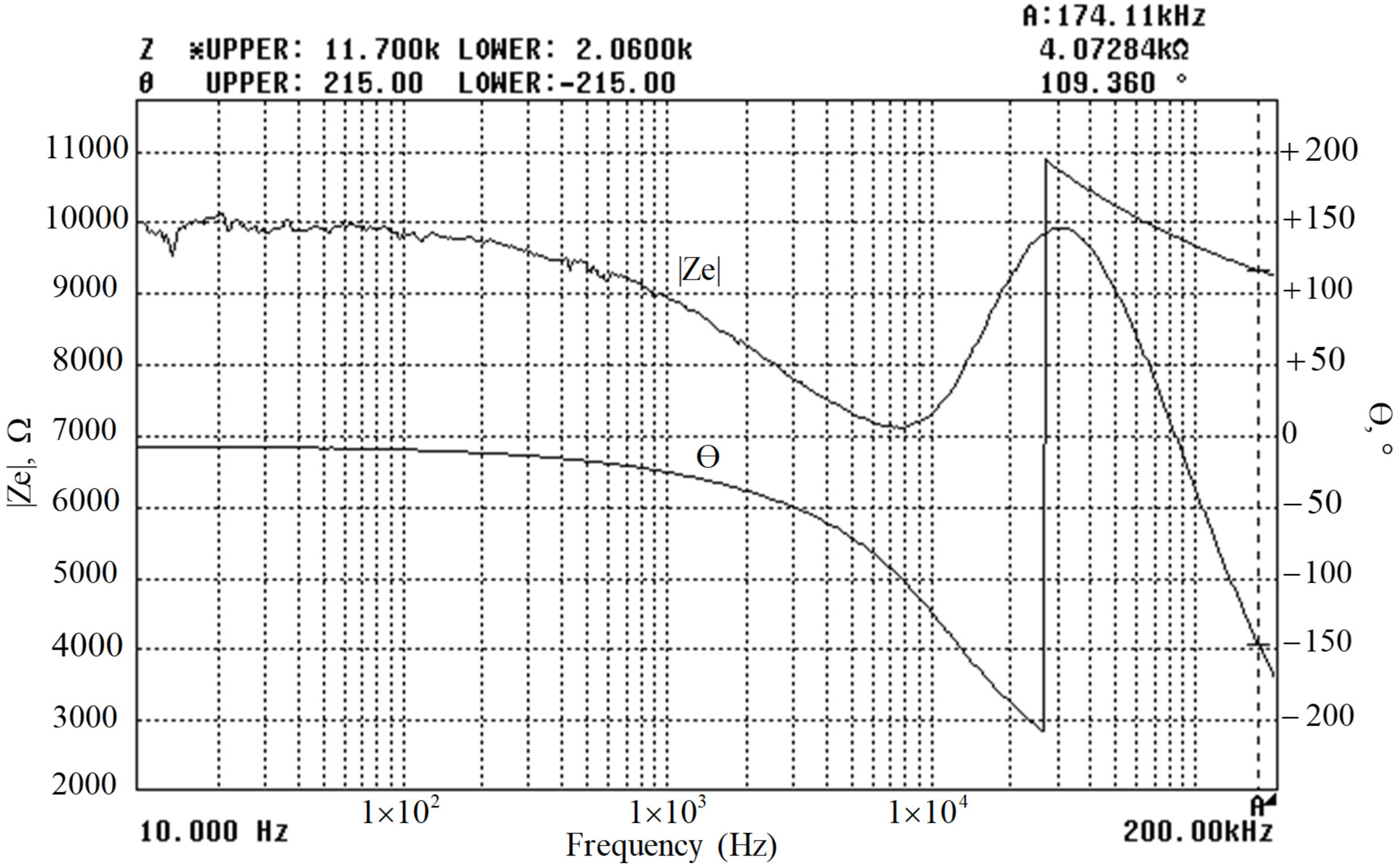
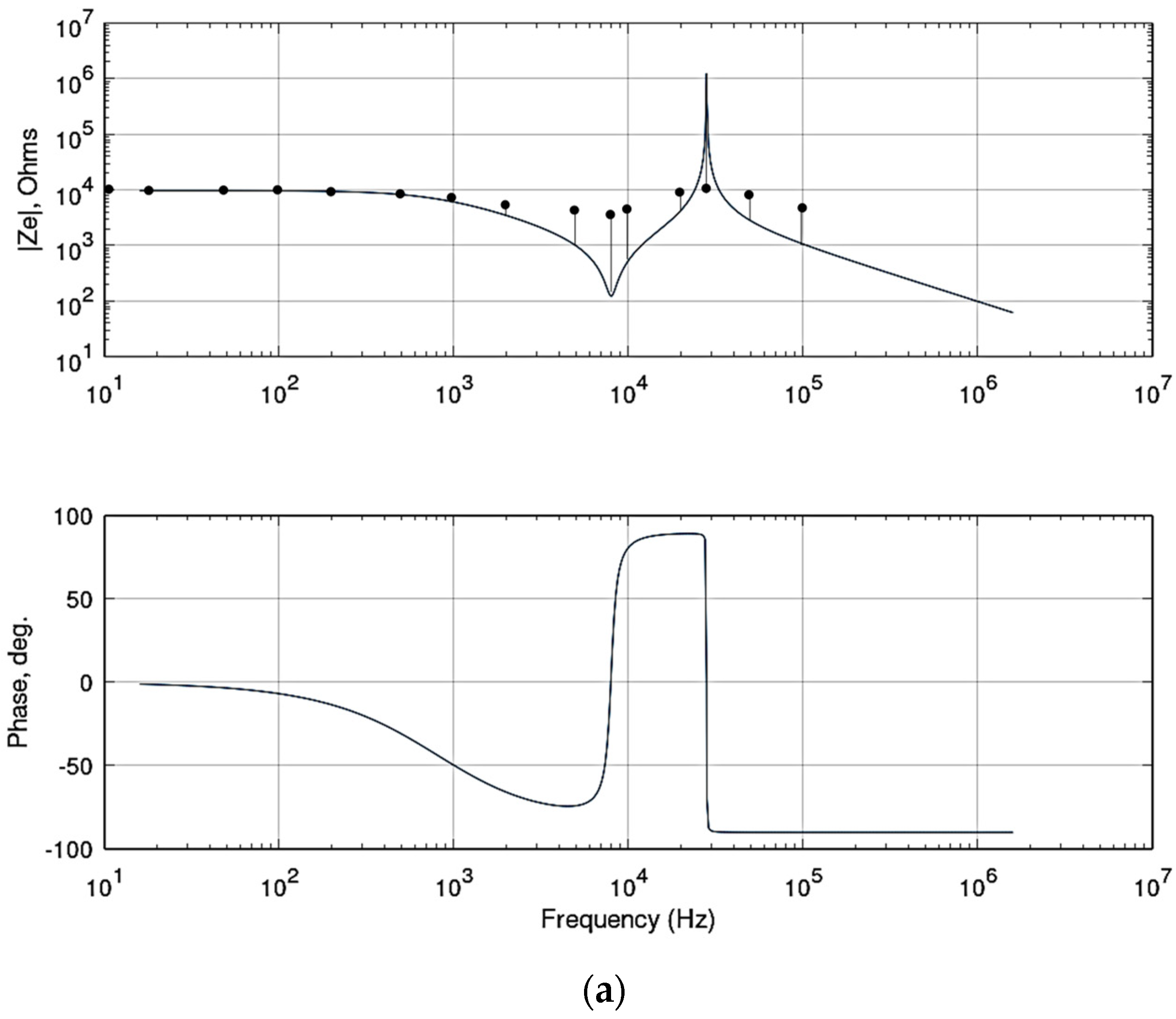
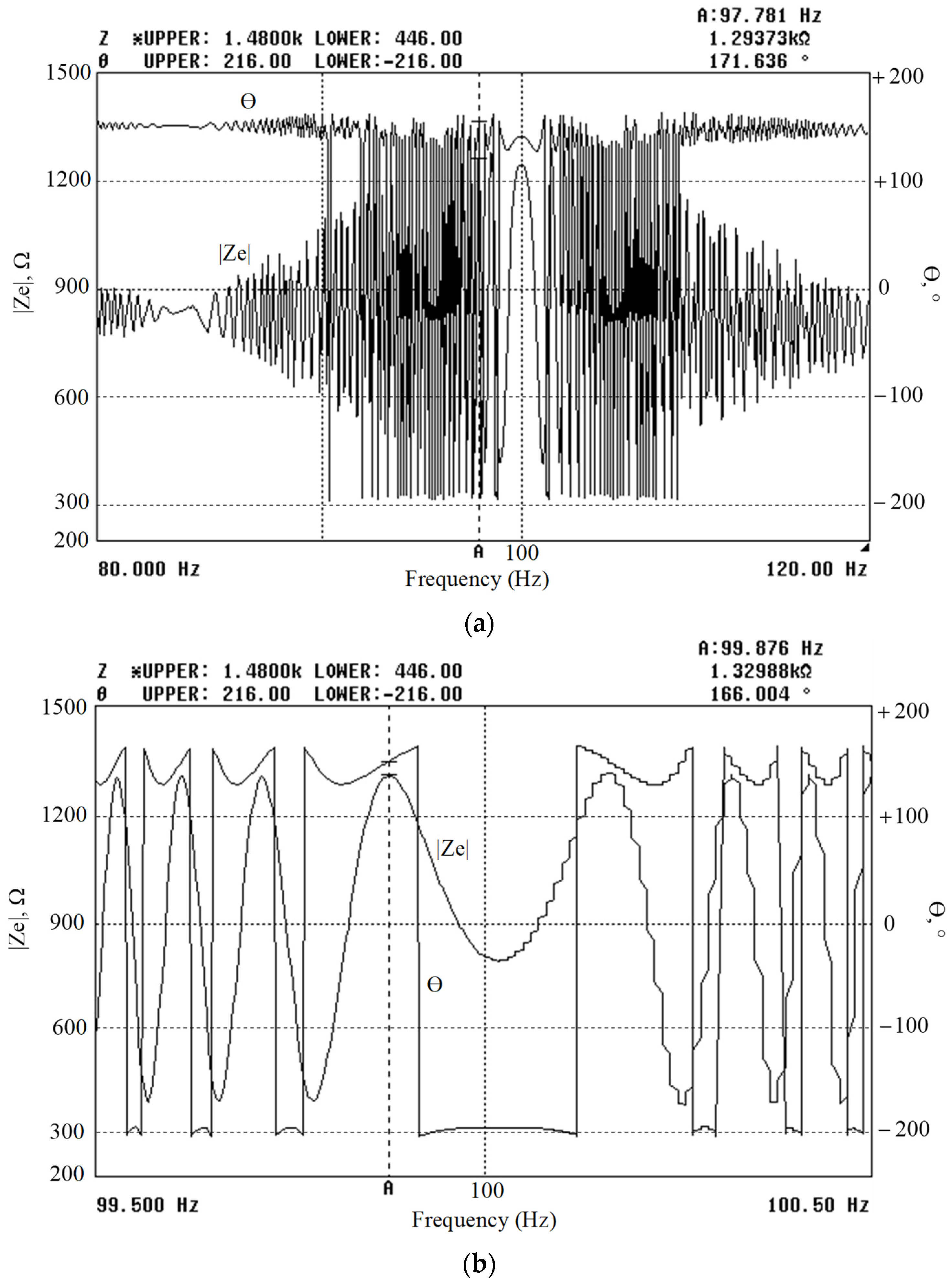
The analysis of the results for the first type of the thin film piezoelectric elements shown in Figure 1 exhibited a pronounced minimum in the transmission coefficient for frequency f s = 8 kHz. In addition, a maximum was obtained at frequency f p = 28 kHz, which defines a parallel resonance. The ohmic resistance at a constant current was 9.64 kΩ. The phase angle, determined by the voltage and current phase, changed its value in the range from 90 ° to + 90 °. This behavior of the impedance characteristic is close to the shape of the quartz resonators characteristics operating in reverse piezoelectric mode. For them, when an alternating voltage is applied between the electrodes, small mechanical oscillations occur, which are proportional to the intensity of the applied electric field (for example, the deformations of the crystal can reach 0.1% of the initial size).
Depending on the shape of the piezoelectric crystal, the planes orientation, the electrodes, etc., different types of oscillations can occur, such as bending, twisting or compressing/stretching. As a result of the vibration of the crystal at a certain frequency, a mechanical series resonance can occur, in which the amplitude of the oscillations becomes maximum, and the electrical resistance between the two electrodes is minimal with typical values of several tens of ohms. The parallel resonance in quartz resonators, for comparison, occurs as a result of the capacitance between the electrodes caused by the dielectric quartz itself and the equivalent quartz inductance. Because the capacitance between the resonator electrodes is significantly greater than the equivalent quartz capacitance, the parallel resonance frequency is higher than the series resonance frequency.
In the studied element, corresponding to Figure 1, a similar behavior was observed, which is repeated in all tested samples of this type. In contrast to classical resonators, the frequency of parallel resonance for the studied element is significantly higher (more than five times) than the frequency of the serial resonance, because the films are thin but deposited on a larger surface.
The impedance characteristics are the basic electrical characteristics that are used to illustrate the functionality of the piezoelectric transducers. In order to fully utilize the benefits of the piezoelectric devices and to ensure their implementation in sensor systems or power electronic converters, the performance has to be fully evaluated. Comprehensive studies are needed if topologies and design solutions are optimized in order to increase the quality factor, to improve the reliability and to adjust the serial and parallel resonance. To ensure reliable operation, the performance of the piezoelectric devices has to be simulated, optimized and experimentally verified by using analytical circuit simulations based on accurate and reliable models of the piezoelectric components. The simulation model of the piezoelectric components should be simple and analytical with a small number of model parameters; however, they have to represent accurately the real impedance characteristics within the simulation environment. Most of the models are based on simple electrical circuits [24,25,26] and contain passive RLC components which are rather easy to implement and suitable in the circuit simulators and at the same time in the mathematical calculation systems, using only few parameters. The parameter extraction procedure of the passive electrical circuits is relatively easy, performed by using measured electrical characteristics.
It was proved that the arbitrary boundary conditions can be artificially controlled to design the equivalent circuit, but it is impossible for a free boundary. In the RLC network, the formula leads to the occurrence of resonances when the boundary condition holds a series of special values with an external AC source. This result suggests the possibility of practical applications of the formula to resonant circuits [27]. The total electrical impedance is the superposition of several physical phenomena coexisting in the device and cannot be related only to the fit to the resonance frequency. Impedance data, in the form of Nyquist plots, which are mainly used at the electrochemical impedance spectroscopy and have been mainly reported in the literature, can help to determine the individual contribution of the phenomena to the global behavior. As is widely known, these plots report the real part of the complex impedance on the x-axis and the imaginary part on the y-axis, taking frequency and DC bias as parameters. However, in a purely electrical impedance study, the contribution of multiple reactive behaviors, rising from the various existing interfaces in the considered device, can be reflected with the help of the phase angle shift, represented with Bode plots. Therefore, it is not possible to find several equivalent models that can be tailored with a simple fit to fulfil the conditions for the same resonant frequency and simultaneously the same phase angle shift.
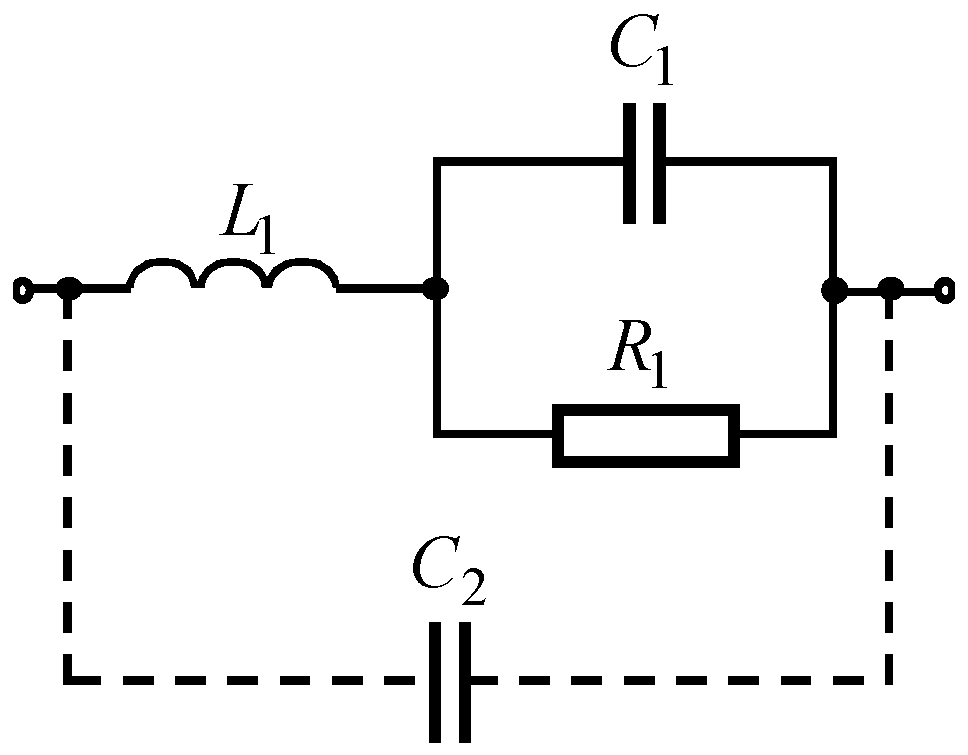
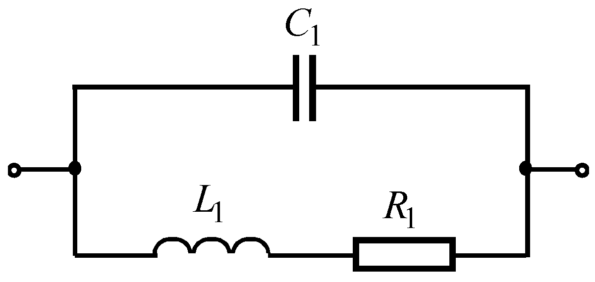
The presented impedance characteristic in Figure 1 can only be obtained with the equivalent circuit diagram given in Figure 2. The proposed electrical circuit in Figure 2 provides a series resonance determined by the inductance L 1 and the capacitor C 1 , with a minimum value of resistance. The ohmic resistance R 1 determines the resistance of the structure to a direct current. In addition, in parallel to the L 1 and C 1 , a capacitance C 2 was added with a dashed line. This capacitance models the behavior of the piezoelectric element when a parallel resonance occurs.
For the circuit in Figure 2, if the capacitance C 2 is neglected, the complex resistance representing the physical structure of the piezo electrical devices with impedance characteristics given in Figure 1 is determined by the expression (Equations (1) and (2)):
Z e = s L 1 + R 1 1 s C 1 ,   or
Z e = R 1 s 2 L 1 C 1 + s L 1 R 1 + 1 s R 1 C 1 + 1 = k T 1 2 s 2 + 2 ξ T 1 s + 1 T 2 s + 1 ,
where k is the DC proportionality constant, T 1 is the time-constant of the polynomic in the numerator, ξ is damping factor and T 2 is the time-constant of the polynomic in the denominator.
From the comparison of the left and right sides of the above equation the following formulas are obtained for the main parameters:
k = R 1 ,   T 1 = L 1 C 1 ,   ξ = 1 2 R 1 L 1 C 1 и   T 2 = R 1 C 1 ,
where L1 is the equivalent series inductance, C1 is equivalent series capacitance, R1 is equivalent parallel resistance, and C2 is equivalent parallel capacitance (parasitic).
Based on the analysis of Equation (2) and the formulas, the basic parameters for the elements in the equivalent circuit and the coefficients of the analytical expression of the complex resistance are obtained: k = R 1 = 9.64 kΩ; ξ = 1 2 Q 0.0562 , where the equivalent quality factor is determined from the following approximate formula Q f s B W 0.7 = 8   kHz 900   Hz 8.89 ( B W 0.7 900   Hz and is defined as the bandwidth at the level of 0.707 from the serial resonance frequency); T 1 = 1 2 π f s = 19.9   μ s ; C 1 = T 1 2 ξ R 1 = 18.45   nF ; L 1 = ( 2 ξ R 1 ) 2 C 1 = 21.66   mH and T 2 = R 1 C 1 = 177.85   μ s . Then, for the complex resistance of the equivalent circuit of Figure 2, the following expression with specific numerical values was obtained (Equation (4)):
Z q = 396.01 × 10 12 s 2 + 2.2367 × 10 6 s + 1 177.85 × 10 6 s + 1 × 9.64   k Ω
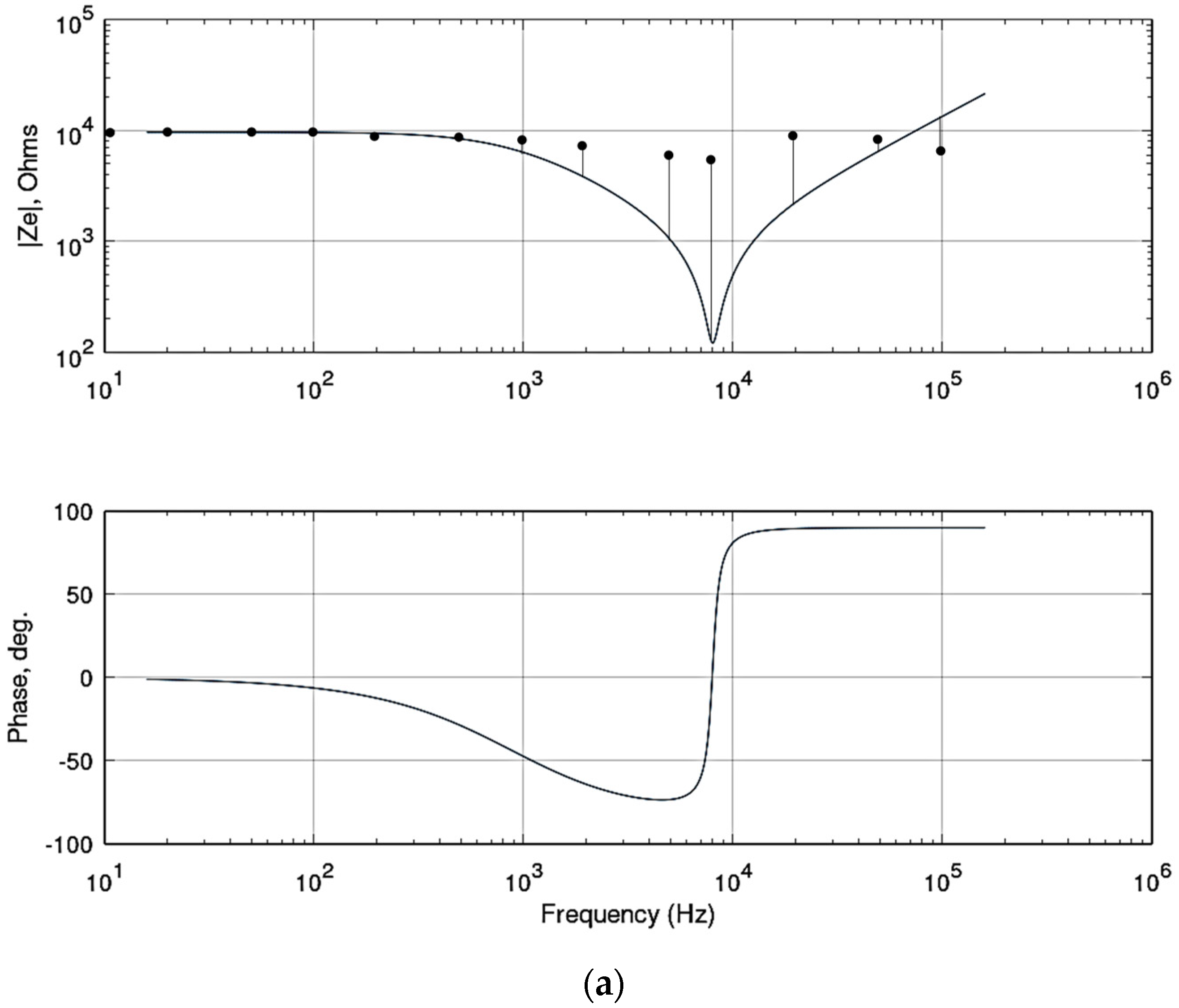
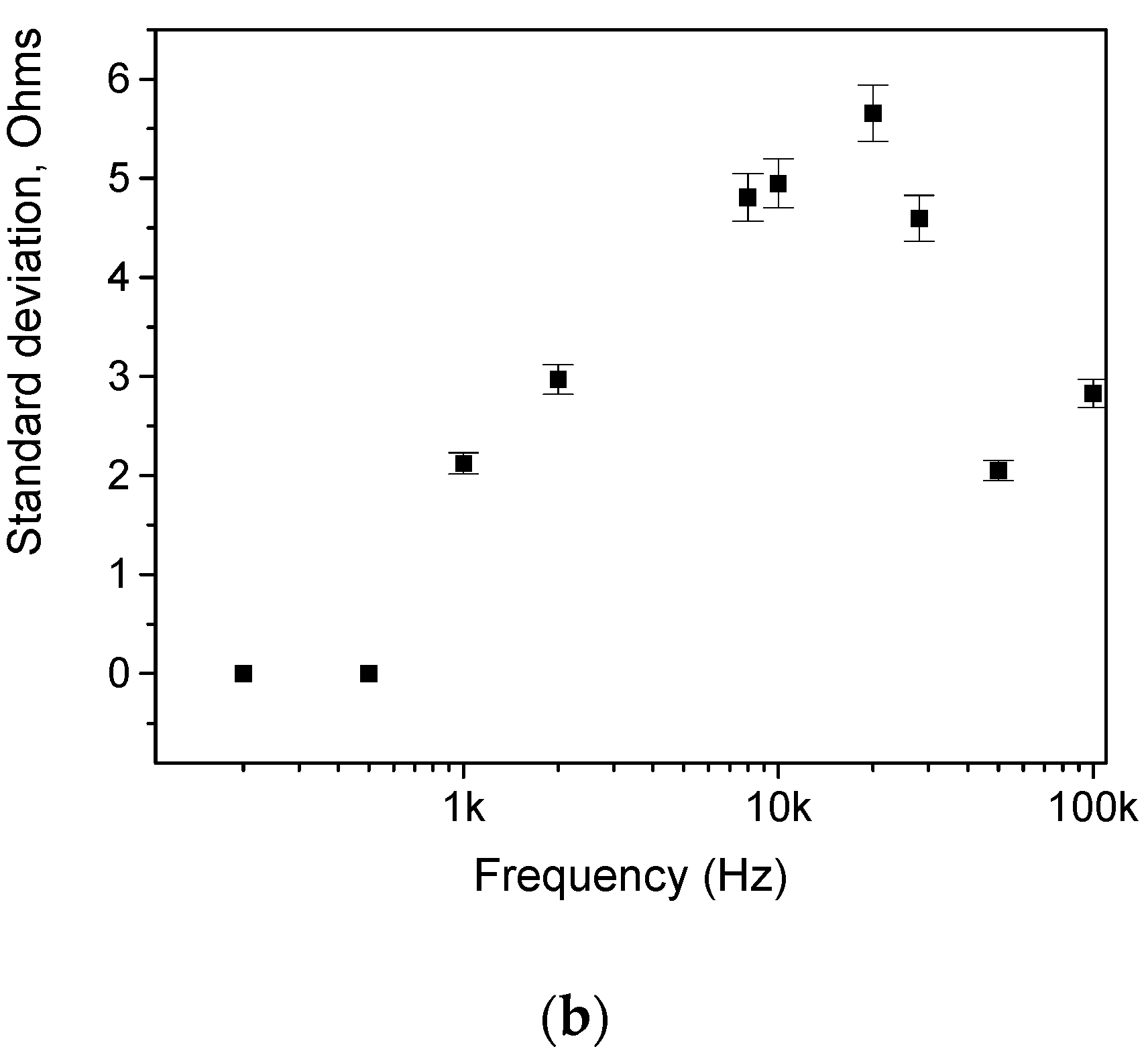
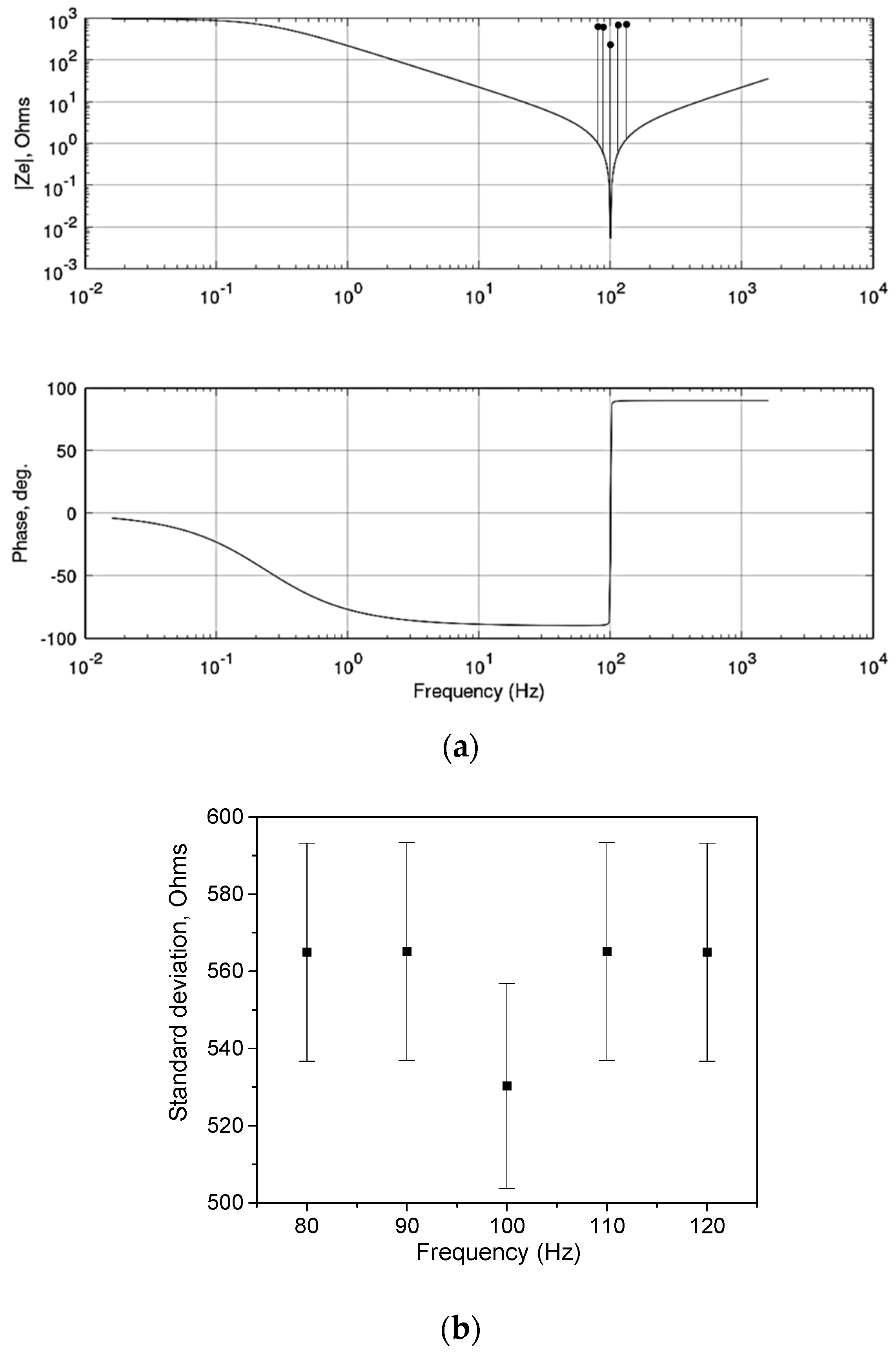
In graphical form, the module and the phase of the complex resistance (Figure 3a) from the above expression are obtained in the environment of the free-to-use program for mathematical calculations Octave [
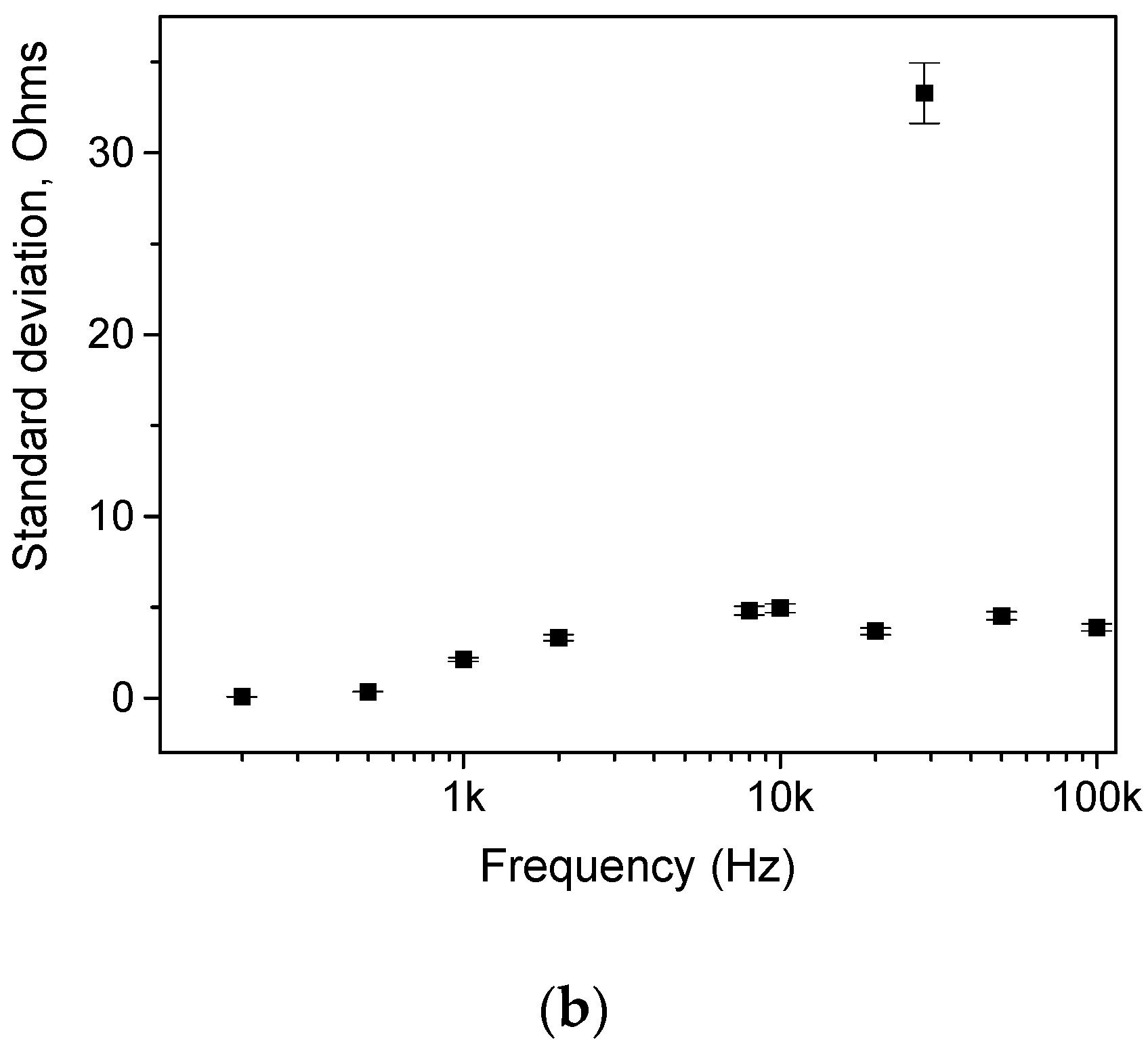
28]. The standard deviation between the measured and modelled curves is presented for specific points extracted from the experimental results in the corresponding frequency range and aligned over the modelled curve for the more critical parameter related to the film’s nature and morphology—the impedance Z (Figure 3b). Its structure, programming language syntax and most of the commands are the same as or similar to those in the MATLAB® programming system. Comparison of the modeled with the experimental characteristics for the module and the phase taking into account the influence of the parallel resonance results in an impedance characteristic determined by the following expression (Equation (5)):
Z e = s 2 L 1 C 1 + s L 1 R 1 + 1 s 3 L 1 C 1 C 2 + s 2 C 2 L 1 R 1 + s ( C 1 + C 2 ) + 1 R 1
The frequency of the parallel resonance is determined considering that R 1 , and the formula is in the form (Equation (6)):
f p 1 2 π L 1 C 1 C 2 C 1 + C 2
The value of the capacitor C 2 can be determined by the formula
C 2 = C 1 ( 2 π f p ) 2 L 1 C 1 1 = 1.6246   nF
The analytical expressions show great overlap between the experiments and the behavior of the models, for both impedance and phase angle. This means that the circuit configuration extracted from the automated procedure is unambiguously suitable for modelling the impedance in the whole frequency range. In general, for a given data set, if there exists more than one equivalent circuit which gives a reasonable fitting, the choice between these has to be based both in simplicity and consistency with the known physical and chemical processes which take place in the system. The best fittings were reached after several attempts. In contrasts to the commercially available transducers, the determination of the equivalent electrical circuits in the software of the impedance analyzer gave significant deviations for the different custom developed thin film piezoelectric structures. Thus, the need for using modified electrical models operating in a strictly defined frequency range appeared. Moreover, based on the analysis of the electrical models, their analytical transfer functions were determined, which were further implemented in a program based on a high-level language, primarily intended for numerical computations. The use of an impedance analyzer for the experimental measurements and mathematics-oriented syntax software for the representation of analytical transmission functions imposed their visualization in separate coordinate systems. Thus, the real measurement values as curves were compared to the equivalent circuit models obtained out of the program environment of the impedance measurement device to guarantee more precisely the correctness of the proposed models choice.
In Figure 4a, the graphical form of the module and the phase of the complex resistance taking into account the parallel resonance is presented (Figure 4b is the standard deviation between the measured and the modelled results for the impedance). The comparative analysis of the two graphs showed that the relative error between the measured and modeled results for the main parameters is not higher than 10%. Such an error is considered acceptable, taking into account the technological tolerances of the parameters, related to the sputtering conditions of the piezoelectric and metallic films growth. In this case, in addition to the serial resonance, a parallel resonance also occurred. Compared to the classical quartz resonators, the difference between the two frequencies in this case is much larger, i.e., the element had a pronounced serial resonance and then had a relatively long region with an inductive resistance.
In summary, according to the observed curves in the Bode plot for Si/Ag/GZO/Ag (Figure 1), the equivalent circuit model involved the resistivity of the piezoelectric film and electrode interfaces, a capacitor formed between the aluminum electrodes formed due to the dielectric permittivity of the GZO film and parasitic inductance of the leads. Additionally, we propose capacitor C2 in parallel to the circuit in order to better reflect the course of the curves. At high frequencies, the current flowing through the interface of the element is not equal to the inner current in the functional film. It is known that the dipoles motion in the thin film cannot well synchronize follow the changes in an electric field of tens kilohertz range for coatings with low dipoles mobility below 30 cm2/(V.s) [29]. This effect is enhanced for the polycrystalline nature of the piezoelectrics and the grains boundaries between the crystallites (or domains). Thus, it can be assumed that space charge accumulated near the electrodes, which is considered as a double layer capacitor [30]. It results in a change of the electric field exhibited as a frequency shift between the impedance and phase angle extremums. Therefore, the double layer was treated as a capacitor in parallel to the basic circuit. This could be the possible reason for reaching the phase angle values greater than 90°. Two extremums of the impedance characteristics can be ascribed to the grain boundaries of the doped piezoceramic, considering that the samples contain two phases (Ga and ZnO).
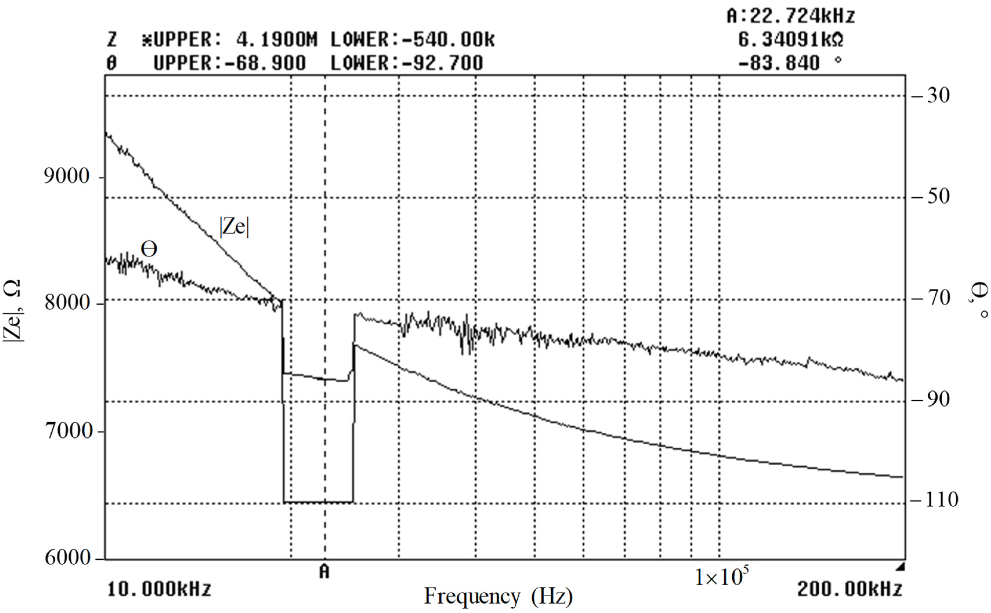
Figure 5 shows the Bode plot for Si/Al/KNbO3/Al with a thickness of the piezoelectric film less than 400 nm.
In comparison with the previous GZO material, no sharp minimum in the Z was observed around 22.72 kHz after its monotonic decrease. Additionally, the phase angle changed in a small range of 68°. This can be ascribed to the lack of a double layer of space charge, respectively, and lack of additional capacitance in the equivalent electrical circuit, modelling the samples behavior. The equivalent circuit from Figure 2 was still valid, but excluding the capacitor C2. In this case, for the elements in the equivalent circuit (Figure 2) and for the coefficients of the analytical expression of the complex resistance it is obtained: k = R 1 = 6.34 kΩ; ξ 0.11 (or Q 4.54 ); T 1 = 7   μ s ; C 1 = 5.018   nF ; L 1 = 9.762   mH , and T 2 = 31.814   μ s . For the complex resistance with specific numerical values, the following was obtained (Equation (8)):
Z q = 49 × 10 12 s 2 + 1.54 × 10 6 s + 1 31.814 × 10 6 s + 1 × 6.34   k Ω
In graphical form, the module and the phase of the complex resistance is shown in Figure 6a (Figure 6b is the standard deviation between the measured and the modelled results for the impedance). A pronounced minimum was exhibited and the phase angle changed from 90 ° to + 90 °. In this case, the quality factor is of the same order as in the previous case. The advantage of this case is the lack of additional parallel resonance, which in the previous case was obtained due to the parasitic capacitor. For this type of element, a pronounced serial resonance was again observed, followed by an area with an approximately linear increase in the reactance.
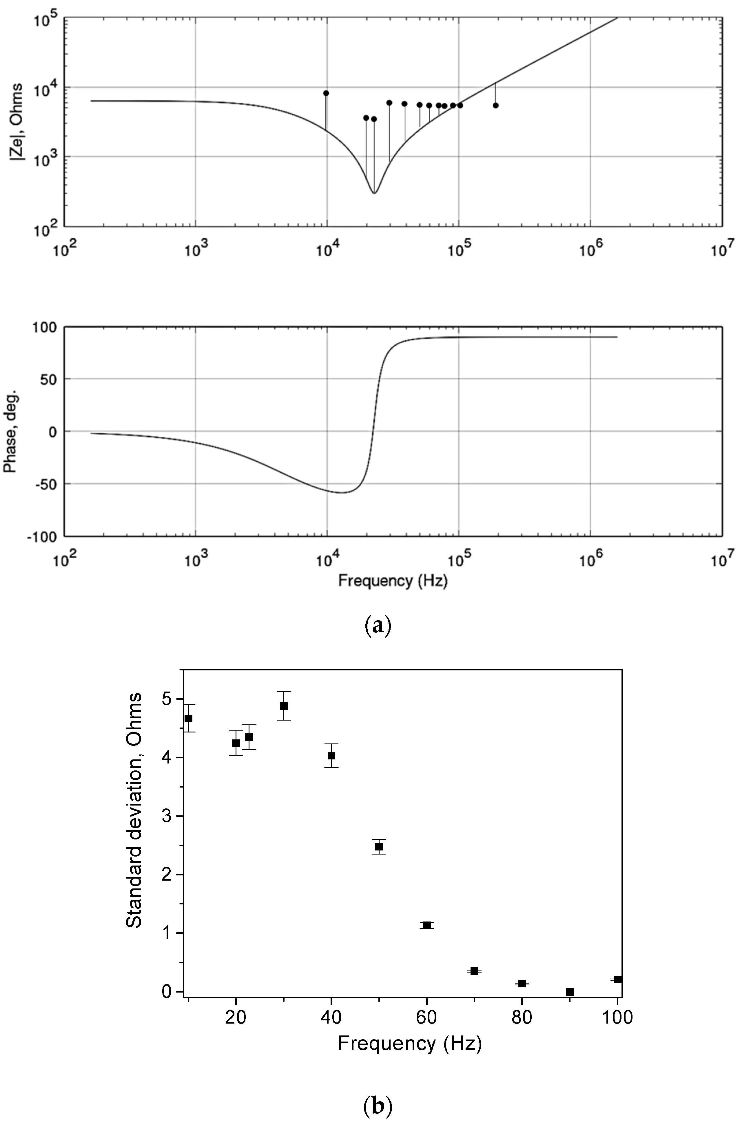
Increasing the KNbO3 film thickness to near 600 nm (thicker film), specific patterns of the impedance characteristics can be noted, which are actually overtone series around the main resonant frequency at 99.8 Hz (Figure 7a,b). Equivalent electrical circuit presented in Figure 2 remained valid. It is known for thicker films that the piezoelectric phenomena are localized in the film bulk rather than distributed between the thin film and the substrate surface [31]. The mechanical waves propagate only in the piezoelectric material and the electrical processes are revealed there instead at the film/substrate interface. Thus, the dominant bulk behavior and the polycrystalline nature of the niobate sputtered films may be responsible for the overtones appearing.
The impedance characteristics of the duplicated KNbO3 based piezoelectric element with thicker film is shown in Figure. 7a, and in its form, a serial resonance and additional parallel resonance were again observed. For the serial resonance was determined a value of 100   Hz , and for the additional parallel resonance was determined a value of 100.11   Hz . In this case, the quality factor for the series resonance was significantly higher and had a value approximately equal to 427. At a constant current, the ohmic resistance was equal to 960   Ω . The parasitic poles and zeros in the impedance characteristic could be ascribed to defects in the film’s microstructure and in the surface monolayers [32]. The characteristic of the complex resistance in a wide frequency range is given in Figure 7b.
For the elements in the equivalent circuit and the coefficients of the analytical expression of the complex resistance was obtained: k = R 1 = 960   Ω ; ξ 1.1709 × 10 3 ; T 1 = 1.5923   ms ; C 1 = 708.3   μ F ; L 1 = 3.58   mH , and T 2 = 679.97   ms . For the complex resistance with specific numerical values was obtained (Equation (9)):
Z q = 2.5354 × 10 6 s 2 + 3.7288 × 10 6 s + 1 679.97 × 10 3 s + 1 × 960   Ω
The module and the phase of the complex resistance are shown in Figure 8a in graphical form (Figure 8b is the standard deviation between the measured and the modelled results for the impedance). The characteristic exhibited a pronounced minimum, and the phase angle changed from 90 ° to + 90 °. Since the transfer function showed only a second-order polynomic in the numerator and a first-order polynomic in the denominator, there were no additional poles and zeros that led to minima and maxima in the impedance characteristic. The slope of the characteristic was high, as the equivalent quality factor had a relatively high value. Compared to the actual characteristic, the additional resonant frequencies were around the main resonant frequency in the range of 80 to 120 Hz. Then, they gradually attenuated and at low frequencies the ohmic resistance was reached, which had a value of about 960   Ω . An advantage in this case is the high quality factor. A disadvantage for this case is the occurrence of additional resonant frequencies, respectively higher or lower than f s 100   Hz .
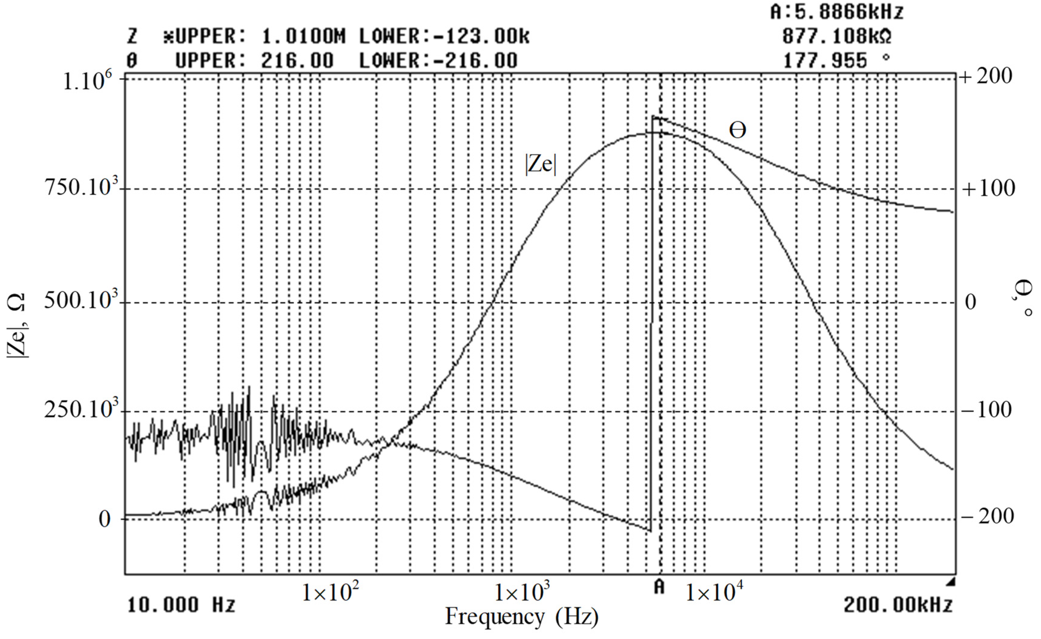
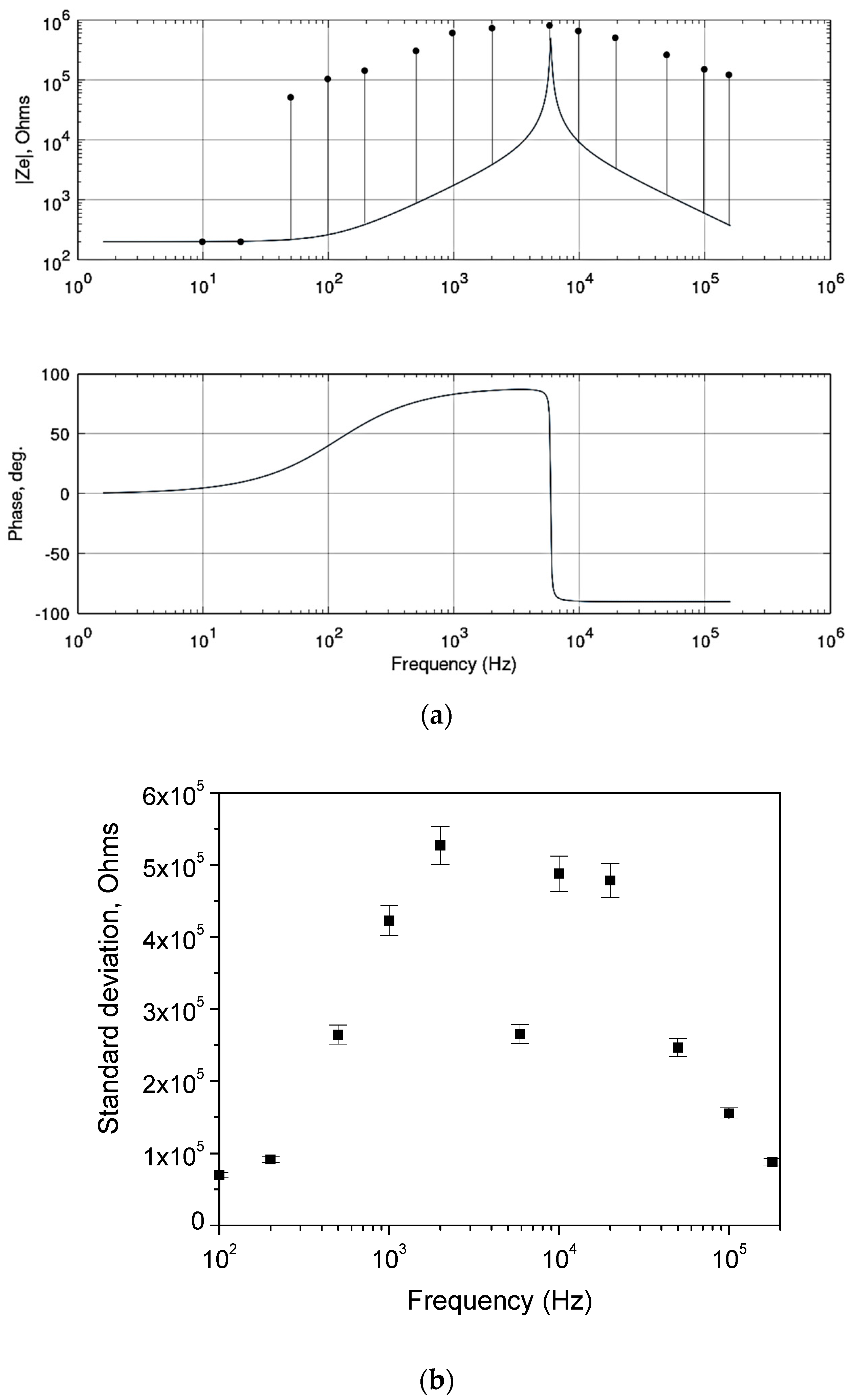
Figure 9 shows a Bode plot for PET/Ag/BST:PVDF-TrFE/Ag. The difference between the concrete values of the resonant frequency, impedance and phase angle is due to the different films’ thicknesses and the electromechanical coupling of the materials. For this reason, only the general tendencies in the curves will be considered. The characteristic resonant frequency was found to be approximately 877 kΩ.
After comparison of the impedance characteristics of the flexible composite based device with those of silicon based samples, it could be noted more clearly defined sharp resonance behavior at the flexible device without additional capacitance effects or double layers. This can be ascribed to the soft matter of the polymeric substrate and the polymeric component of the composite piezoelectric coating, corresponding to constant electric field conditions. Due to their enhanced elasticity, the mechanical wave travelling and the corresponding dipoles distribution process are facilitated as compared to the processes revealing in the solid substrate coated with higher density purely oxide coatings. Thus, because of the specific lattice orientation of the crystalline substances, the electrical and mechanical processes get delay from the applied AC stimulus at the purely oxide piezoelectrics, which is reflected as a frequency shift between the extremums of the measured parameters when the capacitive behavior is dominant [33].
As a general trend, broadening of the peaks could be noted near the characteristic frequency, suggesting spread of the relaxation times, i.e., the existence of electrical relaxation phenomenon in the lead-free piezoelectric materials. The great variation of the phase angle for most of the samples could be an indication of space charge accumulation in the film, serving as defect states with low mobility, causing a relaxation process.

3.2. Devices with Compositional Oxide/Polymer Ferroelectric Coatings

The impedance characteristic shown in Figure 9 can only be obtained with the electrical circuit given in Figure 10. In contrast to the scheme in Figure 2, the proposed electrical circuit in Figure 10 provides a parallel resonance determined by the inductance L 1 and the capacitance C 1 , with maximal value of the resistance r o e = 1 R 1 L 1 C 1 . The ohmic resistance R 1 determines the resistance of the structure at direct current, which is of the order of several hundred ohms.
The presented impedance characteristic (Figure 9) can be explained with the equivalent circuit diagram given in Figure 10 [24,25,26]. Then, the complex resistance was determined by the expression (Equations (10) and (11)):
Z e = ( s L 1 + R 1 ) 1 s C 1 ,   or
Z e = R 1 s L 1 R 1 + 1 s 2 L 1 C 1 + s R 1 C 1 + 1 = k T 1 s + 1 T 2 2 s 2 + 2 ξ T 2 s + 1
From the comparison of the left and right sides of the above equation, the following formulas were obtained for the main parameters: k = R 1 , T 1 = L 1 R 1 , ξ = 1 2 R 1 C 1 L 1 and T 2 = L 1 C 1 , where R1 is the serial resistance of L1, L1 is the parallel equivalent inductance and C1 is the parallel equivalent capacitance. Based on the analysis of Equation (11) and the formulas, the basic parameters for the elements in the equivalent circuit and for the coefficients of the analytical expression of the complex resistance were obtained: k = R 1 = 200   Ω ; ξ 0.01 (or Zmax ≈ 850 kΩ); T 2 = 1 2 π f p = 27.067   μ s ; C 1 = 2 ξ T 2 R 1 = 2.7068   nF ; L 1 = T 2 2 C 1 = 270.68   mH and T 1 = L 1 R 1 = 1.3534   ms . Then, for the complex resistance of the equivalent circuit, the following expression with specific numerical values was applied (Equation (12)):
Z q = 1.3534 × 10 3 s + 1 732.62 × 10 12 s 2 + 541.34 × 10 9 s + 1 × 200   Ω
The module and the phase of the complex resistance were shown in Figure 11a in graphical form (Figure 11b is the standard deviation between the measured and the modelled results for the impedance). A pronounced minimum in the main characteristic was observed, and the phase angle changed from 90 ° to + 90 °. Compared to the impedance characteristic obtained from the measurement, the maximum of the modeled characteristic had a significantly higher value, and an equivalent circuit modeling system with a pronounced resonant character was used. In this case, the quality factor was relatively high, which greatly impaired the output energy maximizing, but the processes revealing in the microstructure best fitted to the processes revealed in the reference piezoelectric crystal plate elements, which is evidenced by the shape of the characteristics closely matched to the reference. It can be assumed that after optimization of the deposition conditions in terms of composition ratios, the quality factor will be sufficiently enhanced without modification of the impedance curves shapes, which is an objective of our future work.
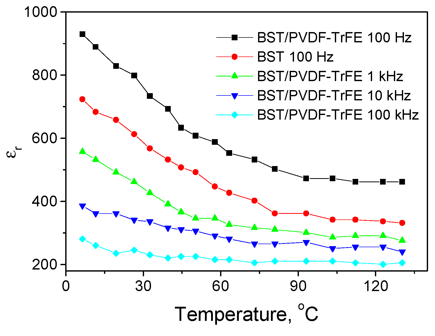
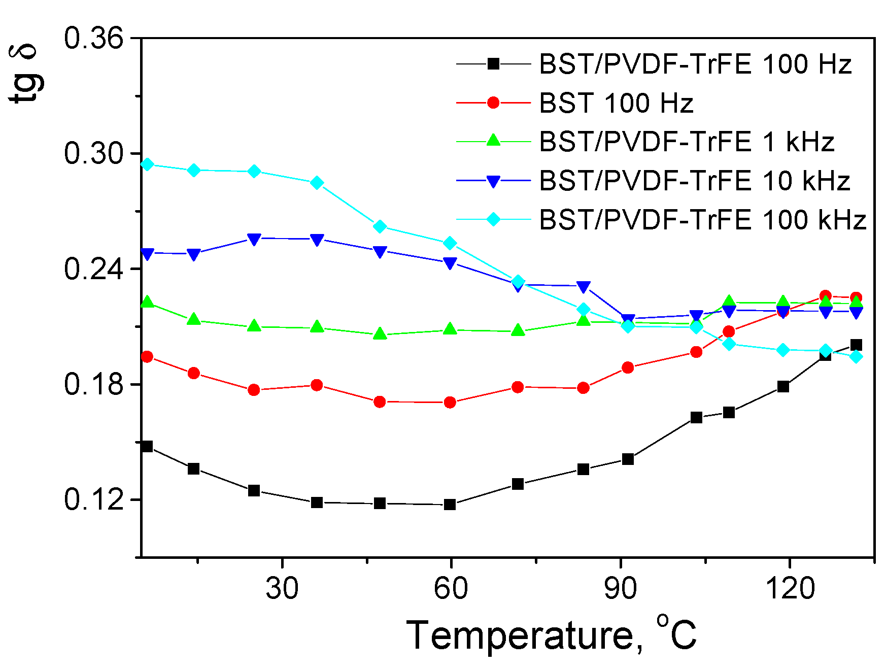
Despite the relatively low quality factor, as the impedance results related to the samples with piezoelectric composite were closest to the shape of the reference characteristics of piezoelectric films, their dielectric behavior was studied more extensively in terms of frequency and temperature dependence of the dielectric permittivity (Figure 12) and dielectric losses (Figure 13).
Dielectric permittivity, εr, and dielectric losses (loss factor), tgδ, were measured within the temperature range from 5 °C to 130 °C (further temperature increase would change the crystal phase of the PVDF-TrFE polymer) at frequencies 100 Hz, 1 kHz, 10 kHz and 100 kHz, for pristine BST sample and PVDF-TrFE/BST. It was found that the dielectric permittivity is greater for the composite PVDF-TrFE/BST that can be ascribed to interfacial polarization at the ceramic/polymer interface due to the difference of their conductivity and piezoelectric coefficients. It was also found that εr slightly decreased with the temperature for all set frequencies (Figure 12). The dielectric permittivity was higher at lower frequencies and was found to decrease monotonically with the frequency. This behavior could be related to the oscillation of the free dipoles in an alternating electrical field, as was predicted in [34,35].
According to some authors, the higher value of dielectric constant at lower frequency is due to the occurrence of different types of polarization, i.e., dipolar, and space charge. Similar to the behavior of dielectric permittivity with frequency, the dielectric loss increased with increasing temperature, except for the frequencies in the range 10–100 kHz, which indicates thermally activation of the dielectric relaxation for the low and middle frequencies.
Dielectric losses were found to be smaller for the PVDF-TrFE/BST, slightly dependent on the temperature and more strongly dependent on the frequency (Figure 13). The results are in good agreement with those reported for ferroelectric composites [37].
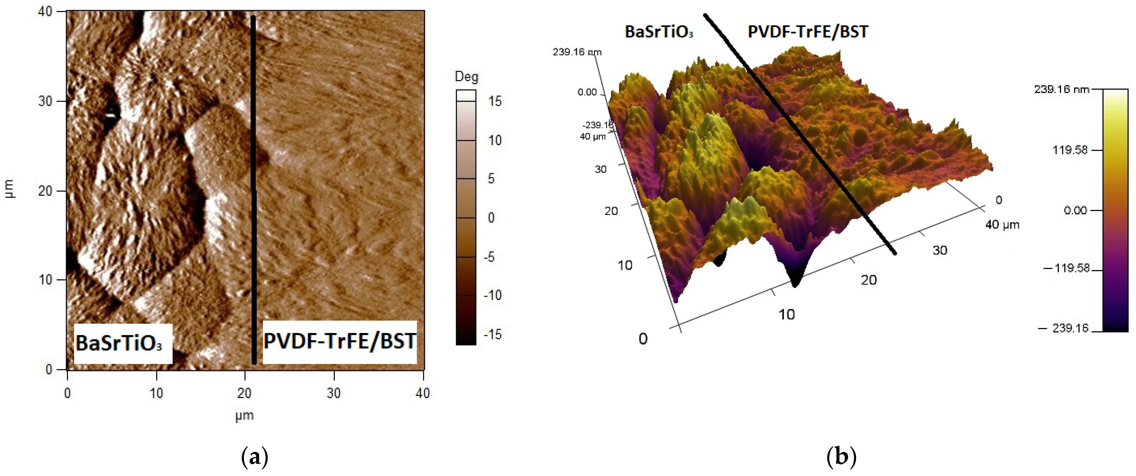
Figure 14 compares 2D and 3D atomic force microscopic (AFM) images of BaSrTiO3 (left half of the images) and PVDF-TrFE coated BST (right half of the images). They reveal that large agglomerates in the range of 10 micrometer grains of perovskite phase are formed at the BST sputtering on the silicon.
On the top view, it seems that a dense microstructure is formed; however, the tilted 3D image shows that there is a great variation in the BST film height at the interface area between the large crystallites (the height difference between the largest hill and hole was approximately 211 nm related to a total thickness of 480 nm). The spin-coating of the polymeric solution caused gaps filling and smoothening of the BST film, as can be clearly seen from both images. Finer microstructure with an average roughness of less than 100 nm was observed for the smoother surface. Then, it is expected that the improved film’s flatness resulted in relatively small losses and contact resistance due to the increased contact area at the interfaces electrode/functional film. This is the reason for the lowest possible measured serial resistance of 200 Ω from the rest samples, containing oxide piezoelectric film only.

4. Conclusions

Impedance spectroscopy has been applied to study thin film lead-free piezoelectric transducers. Identification of the most appropriate equivalent circuit to represent the electrical properties of the samples has been made. Further clarification is necessary to precisely determine the exact contribution of the substrate. It can be concluded that the composite coating exhibited the lowest serial resistance due to the improved morphology after the polymeric ink deposition on the top of the piezoelectric oxide. Although its quality factor is higher, as compared to the GZO film and the thinner KNbO3 film, it should be further enhanced. Comparing the samples with the same material of KNbO3 and different film thicknesses, it can be seen that the greater thickness resulted in decrease of the serial resistance with an order of magnitude, which may be due to the increased density of the coating in this specific case. The thicker one KNbO3 coated on silicon samples exhibited the lowest damping factor with a meaning of the lowest decay rate of oscillation for a long time, resulting in the highest quality factor. In addition, its resonance frequency is the lowest of all the samples, making it more suitable for energy harvesting than for sensing application. The BST/PVDF-TrFE composite material on the other side showed preferable sensing characteristics for fast dynamic pressure changes detection due to the highest resonance frequency and quality factor, as compared to the other high resonance frequency samples (GZO and thin KNbO3). Its dielectric characteristics remained stable in a broad range of temperatures and frequencies.

Author Contributions

Conceptualization, M.A.; methodology, I.P.; validation, M.A. and I.P.; formal analysis, M.A. and I.P.; investigation, M.A. and I.P.; data curation, M.A. and I.P.; writing—original draft preparation, M.A. and I.P.; writing—review and editing, M.A. and I.P.; visualization, M.A. and I.P. All authors have read and agreed to the published version of the manuscript.

Funding

This research was funded by the Bulgarian National Science Fund, grant number KP06-H27/1.

Institutional Review Board Statement

Not applicable.

Informed Consent Statement

Not applicable.

Data Availability Statement

The data presented in this study are available on request from the corresponding author.

Acknowledgments

The authors are thankful to the colleagues from the Bulgarian Academy of Sciences and from the Govt. V.Y.T. Autonomous College, Durg, India for the microscopic imaging of the samples.

Conflicts of Interest

The authors declare no conflict of interest. The funders had no role in the design of the study; in the collection, analyses or interpretation of data; in the writing of the manuscript or in the decision to publish the results.

References

  1. Song, P.; Ma, Z.; Ma, J.; Yang, L.; Wei, J.; Zhao, Y.; Zhang, M.; Yang, F.; Wang, X. Recent progress of miniature MEMS pressure sensors. Micromachines 2020, 11, 56. [Google Scholar] [CrossRef] [Green Version]
  2. Weng, C.-H.; Pillai, G.; Li, S.-S. A thin-film piezoelectric-on-silicon MEMS oscillator for mass sensing applications. IEEE Sens. J. 2020, 20, 7001–7009. [Google Scholar] [CrossRef]
  3. Hartz, J.S.R.; Emanetoglu, N.W.; Howell, C.; Vetelino, J.F. Lateral field excited quartz crystal microbalances for biosensing applications editors-pick. Biointerphases 2020, 15, 030801. [Google Scholar] [CrossRef]
  4. Covaci, C.; Gontean, A. Piezoelectric energy harvesting solutions: A review. Sensors 2020, 20, 3512. [Google Scholar] [CrossRef]
  5. Choudhry, I.; Khalid, H.R.; Lee, H.-K. Flexible piezoelectric transducers for energy harvesting and sensing from human kinematics. ACS Appl. Electron. Mater. 2020, 2, 3346–3357. [Google Scholar] [CrossRef]
  6. Hajra, S.; Sahu, M.; Purohit, V.; Choudhary, R.N.P. Dielectric, conductivity and ferroelectric properties of lead-free electronic ceramic: 0.6Bi(Fe0.98Ga0.02)O3-0.4BaTiO3. Heliyon 2019, 5, e01654. [Google Scholar] [CrossRef] [PubMed] [Green Version]
  7. Huan, Y.; Wang, X.; Li, F.L. Grain size effect on piezoelectric and ferroelectric properties of batio3 ceramics. J. Eur. Ceram. Soc. 2014, 34, 1445–1448. [Google Scholar] [CrossRef]
  8. Ezhilvalavan, S.; Samper, V. Ferroelectric properties and leakage current characteristics of radio-frequency-sputtered SrBi2(V0.1Nb0.9)2O9 thin films. J. Appl. Phys. 2004, 96, 2181. [Google Scholar] [CrossRef]
  9. Kadir, E.S.; Gayen, R.N.; Paul, R.; Biswas, S. Interfacial effects on ferroelectric and dielectric properties of GO reinforced free-standing and flexible PVDF/ZnO composite membranes: Bias dependent impedance spectroscopy. J. Alloys Compd. 2020, 843, 155974. [Google Scholar] [CrossRef]
  10. Kishor Kumar, M.J.; Kalathi, J.T. Investigation on the dielectric performance of PVDF-HFP/LZO composites. J. Alloys Compd. 2020, 843, 155889. [Google Scholar] [CrossRef]
  11. Pandiev, I.; Aleksandrova, M.; Kolev, G. Design and Implementation of Interface Circuits Intended for Printed Piezoelectric Micropower Harvesters on Flexible Substrates. IOP Conf. Ser. Mater. Sci. Eng. 2020, 876, 012007. [Google Scholar] [CrossRef]
  12. Yu, S.; Zhang, C.; Wu, M.; Dong, H.; Li, L. Ultra-high energy density thin-film capacitors with high power density using BaSn0.15Ti0.85O3/Ba0.6Sr0.4TiO3 heterostructure thin films. J. Power Sources 2019, 412, 648–654. [Google Scholar] [CrossRef]
  13. Pozo, B.; de Gorostiza, E.F.; Eletxigerra, U.; Mabe, J.; Martínez, A. Self-powered thin-film impedance spectroscopy sensor system to measure corrosion presence in aerogenerators or aircrafts. In Proceedings of the SPIE (Smart Structures and Materials + Nondestructive Evaluation and Health Monitoring, Online), 27 April–8 May 2020; p. 17. [Google Scholar] [CrossRef]
  14. Omari, L.H.; Moubah, R.; Boutahar, A.; Hajji, L.; El Ouatib, R. Analysis of electrical properties using complex impedance spectroscopy in solid solutions (PbTiO3)0.97-(LaFeO3)0.03 prepared by sol-gel technique. J. Electroceram. 2020, 44, 23–31. [Google Scholar] [CrossRef]
  15. Loyaua, V.; Feuillard, G. Relationship between electrical impedance of a transducer and its electroacoustic behavior: Measurement without primary source. J. Appl. Phys. 2006, 100, 034909. [Google Scholar] [CrossRef]
  16. Arof, A.K.; Amirudin, S.; Yusof, S.Z.; Noor, M. A method based on impedance spectroscopy to determine transport properties of polymer electrolytes. Phys. Chem. Chem. Phys. 2014, 16, 1856–1867. [Google Scholar] [CrossRef] [PubMed] [Green Version]
  17. Gómez-Aguilar, J.F.; Escalante-Martínez, J.E.; Calderón-Ramón, C.; Morales-Mendoza, L.J.; Benavidez-Cruz, M.; Gonzalez-Lee, M. Equivalent circuits applied in electrochemical impedance spectroscopy and fractional derivatives with and without singular kernel. Adv. Math. Phys. 2016, 2016, 9720181. [Google Scholar] [CrossRef] [Green Version]
  18. Calderón-Gutierrez, J.A.; Bedoya-Lora, F.E. Barrier property determination and lifetime prediction by electrochemical impedance spectroscopy of a high performance organic coating. Dyna 2014, 81, 97–106. [Google Scholar] [CrossRef]
  19. Wang, X. BaTiO3/PVDF Nanocomposite film with high energy storage density. APS April Meeting 2016. [Google Scholar]
  20. Aleksandrova, M.; Ivanova, T.; Hamelmann, F.; Strijkova, V.; Gesheva, K. Study of sputtered ZnO:Ga2O3 films for energy harvesting applications. Coatings 2020, 10, 650. [Google Scholar] [CrossRef]
  21. Aleksandrova, M.; Aepuru, R.; Dobrikov, G. Study of printed polymeric flexible energy harvesting elements—Impact of the electrode materials and patterns. IOP Conf. Ser. Mater. Sci. Eng. 2020, 876, 012006. [Google Scholar] [CrossRef]
  22. Tsanev, T.; Aleksandrova, M.; Ivanova, T.; Dobrikov, G. Investigation of lead-free potassium niobate thin films on silicon for piezoelectric transducers. In Proceedings of the X National Conference with International Participation (ELECTRONICA), Sofia, Bulgaria, 16–17 May 2019; pp. 1–4. [Google Scholar] [CrossRef]
  23. Aleksandrova, M.; Tsanev, T.; Dobrikov, G.; Kolev, G.; Sophocleous, M.; Georgiou, J.; Denishev, K. Sputtering of Ga-doped ZnO nanocoatings on silicon for piezoelectric transducers. IOP Conf. Ser. Mater. Sci. Eng. 2019, 618, 012014. [Google Scholar] [CrossRef]
  24. Liang, J.; Liao, W.-H. Impedance analysis for piezoelectric energy harvesting devices under displacement and force excitations. In Proceedings of the 2010 IEEE International Conference on Information and Automation, Harbin, China, 20–23 June 2010; pp. 42–47. [Google Scholar] [CrossRef]
  25. Xing, F.; Dong, B.; Li, Z. Impedance spectroscopic studies of cement-based piezoelectric ceramic composites. Compos. Sci. Technol. 2008, 68, 456–2460. [Google Scholar] [CrossRef]
  26. Yan, F.; Chan, H.L.W. Analytical model of piezoelectric cantilever as rheological sensor. Phys. B Condens. Matter. 2011, 406, 3605–3608. [Google Scholar] [CrossRef]
  27. Tan, Z.-Z.; Zhu, H.; Asad, J.H.; Xu, C.; Tang, H. Characteristic of the equivalent impedance for an m×n RLC network with an arbitrary boundary. Front. Inform. Technol. Electron. Eng. 2017, 18, 2070–2081. [Google Scholar] [CrossRef]
  28. GNU Octave. Available online: https://www.gnu.org/software/octave/ (accessed on 17 November 2020).
  29. Gaspera, E.D.; Bersani, M.; Cittadini, M.; Guglielmi, M.; Pagani, D.; Noriega, R.; Mehra, S.; Salleo, A.; Martucci, A. Low-temperature processed Ga-doped ZnO coatings from colloidal Inks. J. Am. Chem. Soc. 2013, 135, 3439–3448. [Google Scholar] [CrossRef] [PubMed]
  30. Vicentini, R.; Da Silva, L.M.; Cecilio Junior, E.P.; Alves, T.A.; Nunes, W.G.; Zanin, H. How to measure and calculate equivalent seriesresistance of electric double-layer capacitors. Molecules 2019, 24, 1452. [Google Scholar] [CrossRef] [Green Version]
  31. Ion, V.; Craciun, F.; Scarisoreanu, N.D.; Moldovan, A.; Andrei, A.; Birjega, R.; Ghica, C.; Di Pietrantonio, F.; Cannata, D.; Benetti, M.; et al. Impact of thickness variation on structural, dielectric and piezoelectric properties of (Ba,Ca)(Ti,Zr)O3 epitaxial thin films. Sci. Rep. 2018, 8, 2056–2065. [Google Scholar] [CrossRef] [Green Version]
  32. Rehman, F.; Lin, J.B.; Cao, M.-S.; Zhao, Y.-J.; Rizwan, M.; Jin, H.-B. Contribution of grains and grain boundaries to dielectric relaxations and conduction of Aurivillius Bi4Ti2Fe0.5Nb0.5O12 ceramics. Ceram. Int. 2015, 41, 14652–14659. [Google Scholar] [CrossRef]
  33. Cseresnyés, I.; Rajkai, K.; Vozáry, E. Role of phase angle measurement in electrical impedance spectroscopy. Int. Agrophys. 2013, 27, 377–382. [Google Scholar] [CrossRef] [Green Version]
  34. Cassiède, M.; Daridon, J.-L.; Paillol, J.H.; Pauly, J. Impedance analysis for characterizing the influence of hydrostatic pressure on piezoelectric quartz crystal sensors. J. Appl. Phys. 2010, 108, 034505. [Google Scholar] [CrossRef]
  35. Nayak, P.; Badapanda, T.; Pattanayak, R.; Mishra, A.; Anwar, S.; Sahoo, P.; Panigrahi, S. Structural, electrical, and optical behavior of strontium bismuth titanate ceramic. Metall. Mater. Trans. A 2014, 45, 2132–2141. [Google Scholar] [CrossRef]
  36. Aleksandrova, M.; Tsanev, T.; Pandiev, I.; Dobrikov, G. Study of lead-free ferroelectric composite coatings by impedance spectroscopy. Mater. Proc. 2020, 2, 11. [Google Scholar] [CrossRef]
  37. Gautam, C.R.; Kumar, D.; Singh, P.; Parkash, O. Study of impedance spectroscopy of ferroelectric (PbSr)TiO3 glass ceramic system with addition of La2O3. ISRN Spectrosc. 2012, 2012, 410583. [Google Scholar] [CrossRef] [Green Version]
Figure 1. Impedance Z and phase angle θ against frequency for a sample Si/Ag/GZO/Ag.
Coatings 11 00221 g001
Figure 2. Equivalent circuit model, for a solid state substrate samples with GZO piezoelectric films.
Coatings 11 00221 g002
Figure 3. (a) Modelled characteristics of the module and the phase of the complex resistance for the equivalent circuit in Figure 2; (b) standard deviation between experimental and modelled curves.
Coatings 11 00221 g003aCoatings 11 00221 g003b
Figure 4. (a) Modelled characteristics of the modulus and the phase of the complex resistance taking into account the parallel resonance for an equivalent circuit from Figure 2 with capacitor; (b) standard deviation between experimental and modelled curves.
Coatings 11 00221 g004aCoatings 11 00221 g004b
Figure 5. Impedance Z and phase angle θ against frequency for a sample Si/Al/KNbO3/Al with thin potassium niobate (KNbO3) film.
Coatings 11 00221 g005
Figure 6. (a) Modelled characteristics of the module and the phase of the complex resistance for the equivalent circuit from Figure 2 for the case of KNbO3 thinner film based piezoelectric transducer; (b) standard deviation between experimental and modelled curves.
Coatings 11 00221 g006
Figure 7. Impedance Z and phase angle θ against frequency for a sample Si/Ag/KNbO3/Ag with thicker KNbO3 film: (a) general view and (b) re-scaled closer view.
Coatings 11 00221 g007
Figure 8. (a) Modelled characteristics of the module and the phase of the complex resistance for the equivalent circuit from Figure 2 for the case of KNbO3 thicker film based piezoelectric transducer; (b) standard deviation between experimental and modelled curves.
Coatings 11 00221 g008
Figure 9. Impedance Z and phase angle θ against frequency for a sample PET/Ag/BST:PVDF-TrFE/Ag.
Coatings 11 00221 g009
Figure 10. Equivalent circuit model of the flexible substrate based samples with composite piezoelectric films.
Coatings 11 00221 g010
Figure 11. (a) Modelling characteristics of the module and the phase of the complex resistance for the equivalent circuit shown in Figure 10; (b) standard deviation between experimental and modelled curves.
Coatings 11 00221 g011
Figure 12. Variation of the permittivity with the temperature, frequency and composition of the functional film [36].
Coatings 11 00221 g012
Figure 13. Variation of the loss factor with the temperature, frequency and composition of the functional film [36].
Coatings 11 00221 g013
Figure 14. AFM images comparing the surface topography of BST film and PVDF-TrFE coated BST film: (a) 2D (top view); (b) 3D view of the same surfaces [36].
Coatings 11 00221 g014
Publisher’s Note: MDPI stays neutral with regard to jurisdictional claims in published maps and institutional affiliations.

