Properties of Bare and Thin-Film-Covered GaN(0001) Surfaces


1
Institute of Experimental Physics, University of Wrocław, pl. M. Borna 9, 50-204 Wrocław, Poland
2
Łukasiewicz Research Network–PORT Polish Center for Technology Development, ul. Stabłowicka 147, 54-066 Wrocław, Poland
Coatings 2021, 11(2), 145; https://doi.org/10.3390/coatings11020145
Submission received: 30 December 2020
/
Revised: 20 January 2021
/
Accepted: 21 January 2021
/
Published: 28 January 2021
(This article belongs to the Special Issue Selected Papers from the 2nd Coatings and Interfaces Web Conference (CIWC2020))
Abstract
:In this paper, the surface properties of bare and film-covered gallium nitride (GaN) in wurtzite form, (0001) oriented, are summarized. Thin films of several elements—manganese, nickel, palladium, arsenic, and antimony—were formed by the physical vapor deposition method. The results of the bare surfaces, as well as the thin film/GaN(0001) phase boundaries presented, were characterized by X-ray and ultraviolet photoelectron spectroscopies (XPS, UPS). Basic information on the electronic properties of GaN(0001) surfaces are shown. Different behaviors of the thin films, after postdeposition annealing in ultrahigh vacuum conditions such as surface alloying and subsurface dissolving and desorbing, were found. The metal films formed surface alloys with gallium (MnGa, NiGa, PdGa), while the semimetal (As, Sb) layers easily evaporate from the GaN(0001) surface. However, the layer in direct contact with the substrate could react with it, modifying the surface properties of GaN(0001).
1. Introduction
The intensive development of research related to gallium nitride (GaN) arose in the second half of the 1990s. This was due to the improvement in GaN crystal quality and their availability on the market, which opened the door for wide use in modern electronic devices [1,2,3]. The upward trend of research continues to this day, proving the attractiveness of this semiconductor. This stems from the fact that GaN, especially in the wurtzite structure, has many more potential applications in the light-emitter, high-power, and high-frequency fields compared to the conventional III-V semiconductors, i.e., GaAs, GaSb [4,5,6,7,8,9,10]. This is due to its unique physicochemical properties, such as a wide and direct bandgap, along with high electron mobility, thermal conductivity, and breakdown voltage. Furthermore, GaN, due to its high chemical and thermal resistance, enables electronic equipment to operate under harsh conditions, in contrast to electronic devices based on the well-established silicon or germanium semiconductors. In the development of research topics related to GaN, a breakthrough moment was the mastering of the technique of doping this semiconductor, in particular to the p-type. These discoveries have directly contributed to the possibility of producing electronic devices, including diodes emitting blue light, for which Akasaki, Amano, and Nakamura were awarded the Nobel Prize in 2014. The high popularity of GaN-based materials is also due to the easy method of band structure tuning by substituting one of the elements for another from the same atomic group, creating a new III–N alloy in the wurtzite form [8,10]. The operation of a GaN-based device depends on the quality of the heterostructures, which, in turn, is subject to the initial GaN surface. The (0001) surface, terminated with gallium atoms, is the most commonly used form of GaN in the electronics industry; therefore, it is important to gain a deep insight into the properties of GaN(0001) surfaces. In turn, the properties of thin-film systems, especially the metallic films deposited on semiconductors, are also extremely important because they are the basic and necessary parts of all electronic structures. A simple device, i.e., the contact, plays a crucial role in the functionality of electronic components and may show different electrical behaviors. It can have the Ohmic or Schottky characteristic. However, both these types are extremely substantial for electronics. The contact behavior for the GaN-based electronic device is determined by the properties of the thin-film/GaN phase boundary, which depends on the properties of the bare GaN(0001) surface itself and the characteristics of the deposited material. Manganese (Mn), nickel (Ni), and palladium (Pd) are present in many electronic devices [9]. It was found that Mn is a very attractive material for creating a ferromagnetic MnGaN semiconductor by molecular beam epitaxy (MBE) [11,12] and, therefore, for creating hybrid systems with spintronic potential [13,14]. Mn on GaN was studied using the scanning tunneling microscopy (STM) technique [15,16,17,18,19] as well as by photoemission experiments [20,21,22,23,24]. Thin films of Ni and Pd on GaN were also studied [25,26,27,28,29,30,31]. Due to one of the highest work function values among metallic elements, both Ni and Pd are used as materials or components for making electrical contacts with GaN. Electric contacts using Pd/Ni bilayers improve device performance [32]. The interfacial reaction between nickel and GaN can occur during annealing [33], which is a commonly used step for contact creation. This can lead to the formation of new Ni–Ga alloys (similar to the case of the Pd/GaN interface [34]) that have catalytic potential [35,36,37,38,39,40,41]. This paper presents the nature of the interaction of Ni and Pd atoms with the GaN substrate and the morphological changes of thin films under the influence of annealing.
In addition to metals, another interesting group of materials deposited as thin layers on GaN surfaces is semimetals such as arsenic (As) and antimony (Sb). Processes of MBE growth with As [42,43,44,45] and Sb [46,47] as surfactants were performed to increase the quality of GaN films. Furthermore, as incorporation into GaN changes the electronic properties of the host [48,49,50,51], antimony was also used to modify the properties of GaN [52,53,54] and to form GaNSb films with a p-type character [55,56]. The interaction of As and Sb with GaN, as well as the morphological changes caused by postdeposition annealing, have been studied [57,58], where it was shown that thermal treatment leads to easy desorption of the films, but some adsorbated atoms remain on the surface, modifying its properties.
The basic studies of the interface between GaN and thin layers have attracted a lot of attention in both fundamental and application research. However, in order to interpret them correctly, it is necessary to understand the differences in the electronic structure of bare n-, p-, and nondoped GaN(0001) surfaces. Despite the wide availability of professional literature on these topics and some very good and extensive reviews [59,60,61], there are still papers containing misinterpretations of the basic results obtained in photoemission experiments. This is, among other things, due to (i) the relatively difficult cleaning procedure of the GaN surface, which may lead to changes in its stoichiometry—the bare and metal-covered surface can easily be enriched with gallium [29,34,62], which can lead to a flawed interpretation of the deconvoluted Ga-3d components; (ii) the presence of a large number of Ga Auger lines, which may overlap other core level spectra; (iii) surface photovoltage (SPV) effects, which can cause changes in the Fermi level position versus the valence band maximum [63,64]. Furthermore, SVP can sometimes even lead to the appearance of a quasi-Fermi level in the metal/GaN system [30], which can be mistakenly interpreted as a chemical shift.
Herein, the differences between photoelectron spectra of bare GaN(0001), achieved by three various X-ray sources, i.e., nonmonochromatic Mg Kα (1253.6 eV) and non- and monochromatic Al Kα (1486.7 eV), are presented. The information shows the differences in spectra and is particularly useful for materials research, where the correct interpretation of the results can be problematic. This article also presents a review of the author’s studies on thin films on the GaN(0001) surface, including metals (Mn, Ni) and semimetals (As, Sb). Furthermore, this paper shows three scenarios of thin-film behavior under the influence of annealing in ultrahigh vacuum (UHV) conditions: (i) surface alloying for the Ni, Mn metals; (ii) dissolving in subsurface layers of the substrate, with reference to Mn; (iii) desorbing in the case of the As and Sb semimetals. The results show that the electronic properties of the GaN(0001) surface, obtained after the evaporation of thin films, are modified by dissolution or the presence of a reacted adsorbate layer.
2. Method
All results presented in this paper were obtained on samples of nondoped, n-, and p-type wurtzite GaN(0001) epilayers that had been grown using metal–organic vapor phase epitaxy (MOVPE). The thin films were deposited in a standard UHV chamber using the physical vapor deposition (PVD) method, with the exception of arsenic, which was also deposited by PVD but in an MBE chamber interconnected with an analytic system. The formation and measurements of the thin-film systems were done in situ at room temperature (RT). The physicochemical properties of bare and thin-film-covered GaN(0001) surfaces were obtained by means of X-ray photoelectron spectroscopy (XPS) using nonmonochromatic 1253.6 eV or non- and monochromatic 1486.6 eV photons. The electronic properties were measured using ultraviolet photoelectron spectroscopy (UPS) with a nonmonochromatic excitation source of 21.2 eV. Photoelectrons were collected using hemispherical electron energy working in constant analyzer energy mode (CAE), with a step size of 0.05 or 0.1 eV and pass energy of 20 eV in the case of XPS measurements. A step size of 0.025 eV and pass energy of 2 eV were applied for UPS experiments. All binding energies (BEs) were referred to the Fermi level (EF), the position of which was determined using an Ar-ion-cleaned reference Ag sample. No charge effect of the samples was observed; thus, no BE corrections were performed for the presented data. The structural analysis presented herein was carried out using the low-energy electron diffraction (LEED) technique. In the research regarding the properties of a bare GaN surface, a Kelvin probe was also used.
3. Results and Discussion
3.1. Bare GaN(0001) Surface
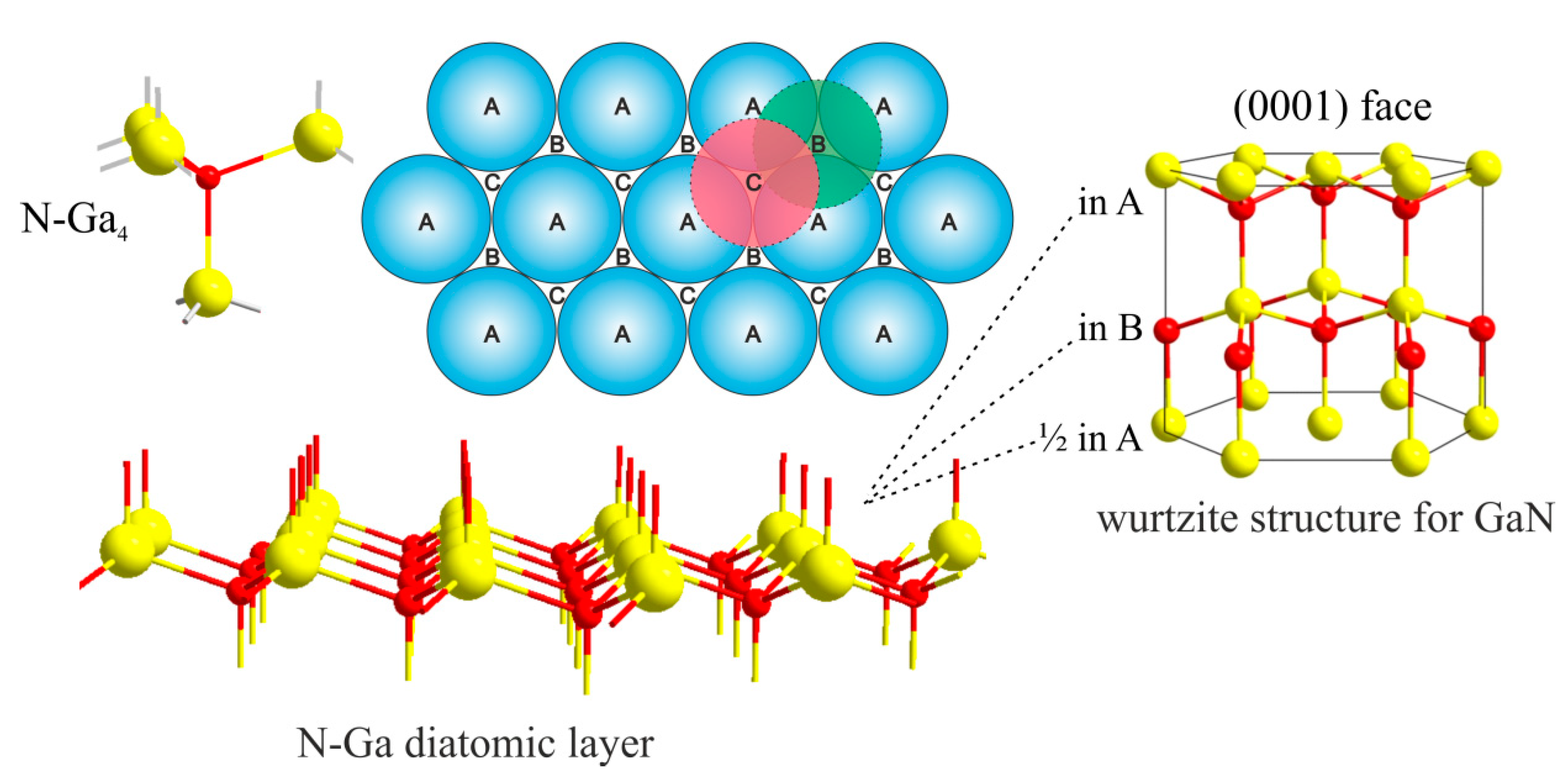
The GaN material contains gallium and nitrogen atoms in 1:1 stoichiometry, forming the hexagonal N-Ga diatomic layer in which the atoms are arranged in imperfect tetrahedral geometry due to different atom sizes and the electronegativity of Ga and N atoms. The hexagonal N-Ga diatomic layers, forming an hcp structure, can be stacked on top of each other in the c-direction, taking places A, B, or C, as shown in Figure 1. There are two stable GaN structures with the ABAB … or ABCABC … stacking sequences, for which GaN crystals are obtained in the form of the wurtzite- or zinc-blend, respectively. In addition to being different in structure, both materials have other electronic properties [65,66,67,68]. GaN(0001) has the wurtzite form and is terminated with Ga atoms, unlike the (000) surface, on top of which N atoms are situated.
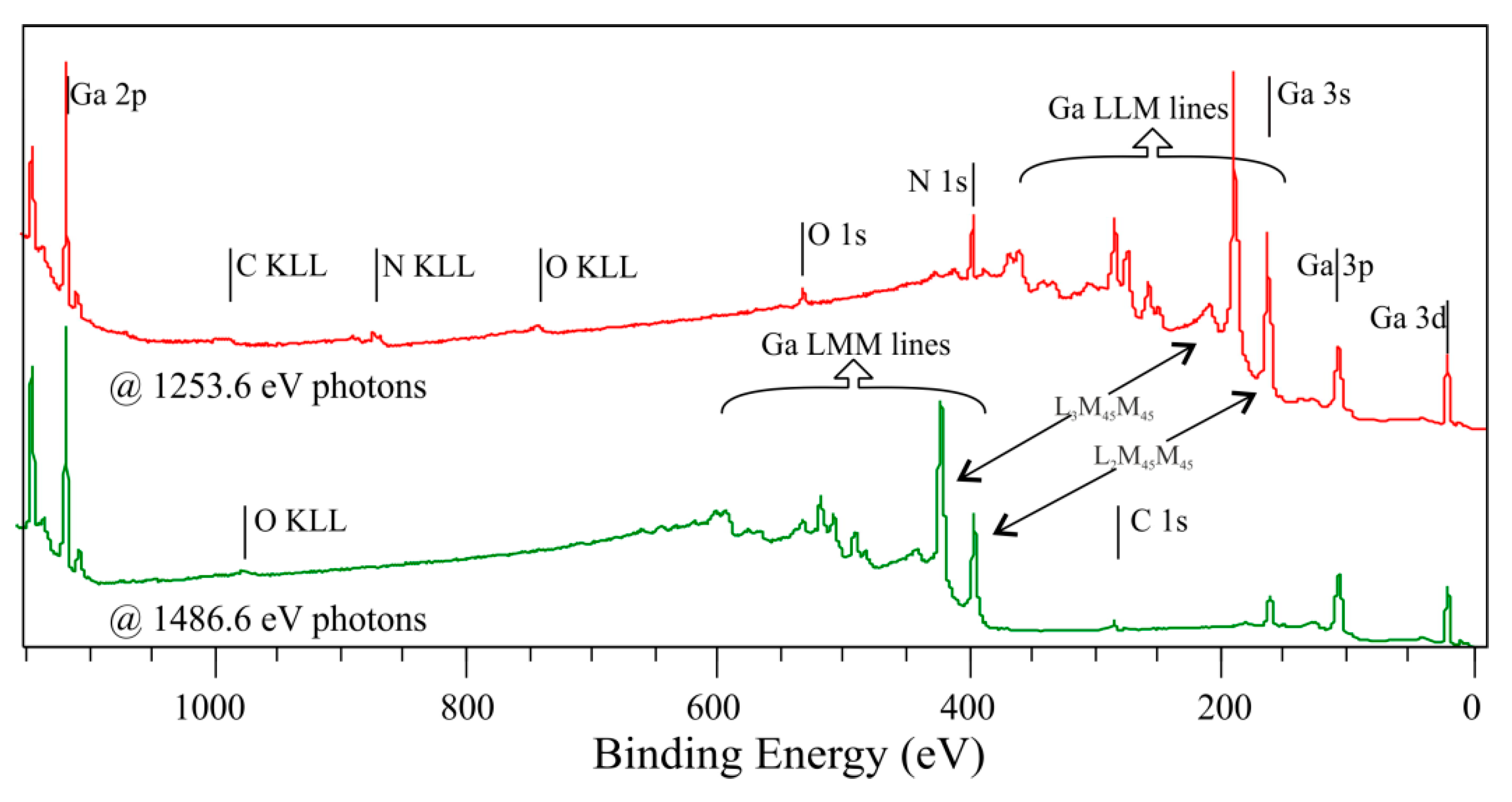
Below are the results of the nondoped (0001)-oriented GaN sample, precleaned with isopropanol, then cleaned in situ using short-time annealing under UHV conditions at a temperature of about 800 °C. The broad XPS spectra of the sample, obtained with 1253.6 and 1486.7 eV photons, are shown in Figure 1. Besides the Ga-2p, Ga-3s, Ga-3p, N-1s peaks from GaN, the C-1s, O-1s core-level lines that are derived from carbon and oxygen impurities are also visible. Auger electrons emitted from a sample exposed to X-rays also contribute to the collected spectra. They form characteristic energy levels from Auger transitions in atoms presented on surfaces and subsurface layers. In Figure 2, there are many electrons from Ga LLM transitions, especially two intensive levels, i.e., L3M45M45 and L2M45M45, with kinetic energies of about 1065 and 1091 eV, respectively. It is also worth noting that the kinetic energy of Auger electrons does not depend on the energy of excitation radiation (unlike photoelectrons). Thus, the same Auger levels in spectra obtained with different photon energies are located at different spots of the BE, as shown in Figure 2. Furthermore, in the case of measurements with the Mg Kα excitation line, carbon content on GaN surfaces cannot be determined because the C-1s line is covered by one of the Ga LMM levels. For experiments with Al Kα photons, the N-1s line partly overlaps with the Auger signal.
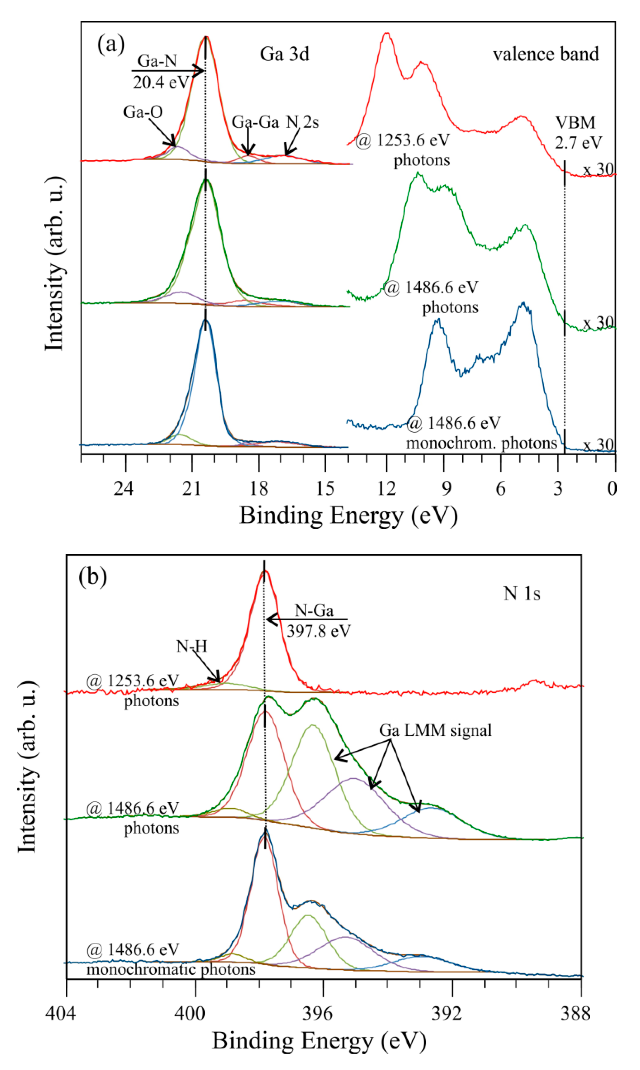
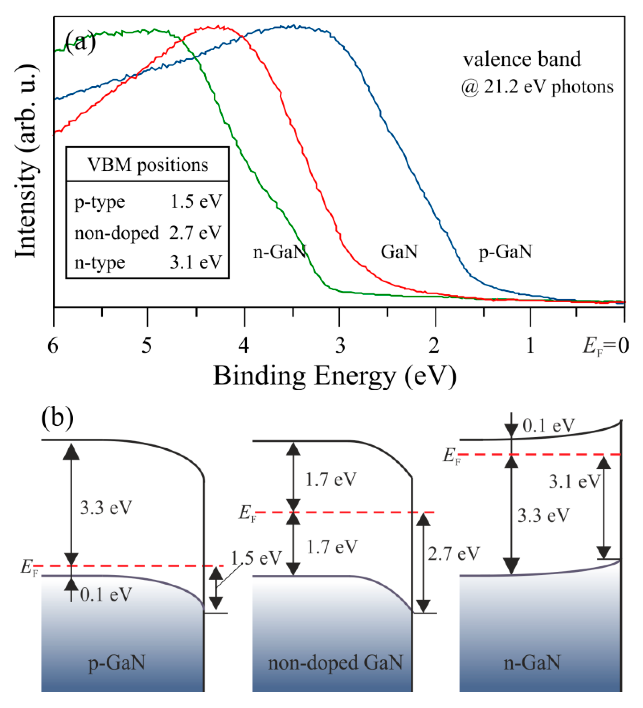
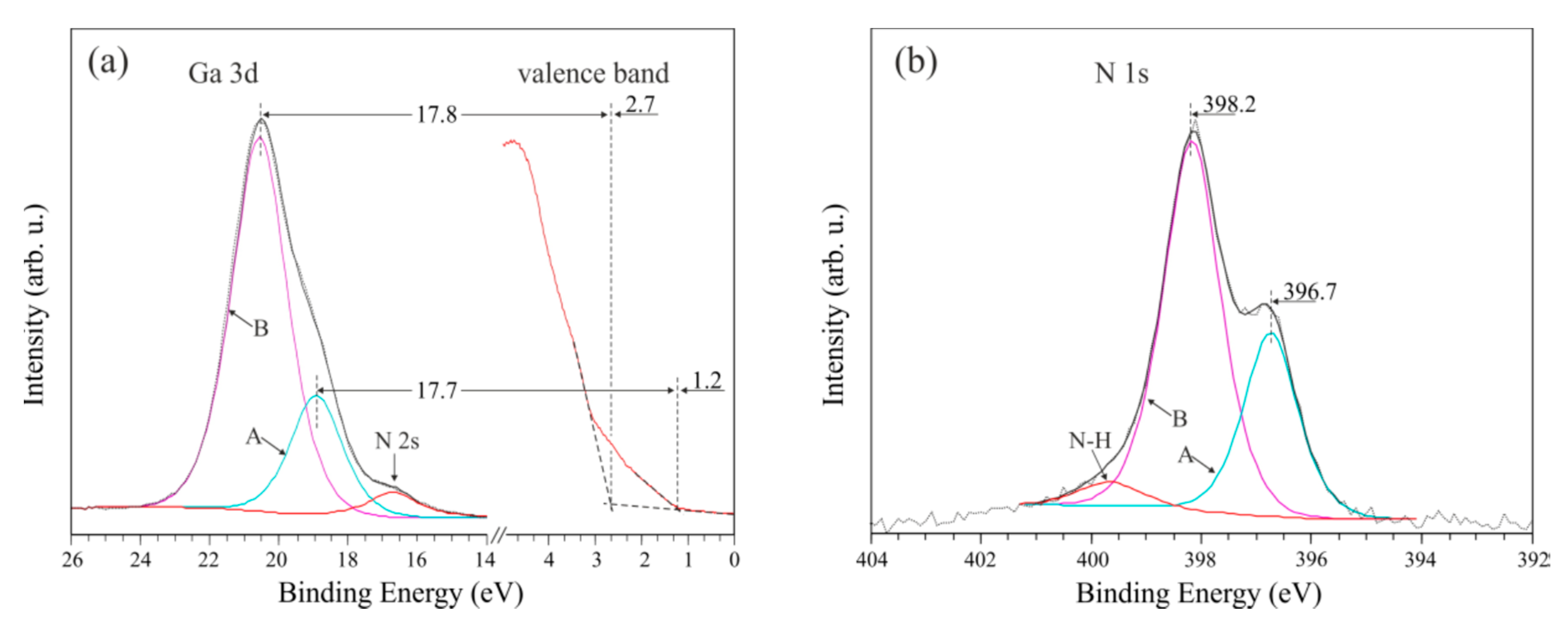
The influence of standard commonly used radiation sources on the obtained spectra shape is shown in Figure 3. On the GaN(0001) surface, where a trace amount of oxygen is present, the Ga-3d shallow core-level line with a BE of 20.4 V contains four subpeaks. The main one is from the Ga–N bonds, while the other two correspond to Ga–O and Ga–Ga bonds and the last one comes from the overlap N-2s state [22,51,69]. The X-ray source type has little effect on the shape of the Ga-3d peaks obtained, but this is not the case for the valence band (VB), where the impact is significant, as shown in Figure 3a. This is due to the overlap of the X-ray satellite of the Ga-3d peak on the VB, measured with nonmonochromatic sources, and the different depths from which the electrons originate. The kinetic energy of ejected electrons from the VB, excited with 1253.6 eV (Mg Kα) and 1486.7 eV (Al Kα) photons, varies significantly, causing them to have different inelastic mean free paths. This results in signals collected with different photon sources coming from various sample depths.
Despite different shapes, the valence band maximum (VBM) is located 2.7 eV below the EF and is found from a linear extrapolation of the leading edge of the spectrum to the background. In Figure 3b, the N-1s spectrum collected with Mg Kα photons consists of two elements: one is assigned to the N–Ga bonding with the BE of 397.8 eV and the other to N–H bonds. This spectrum, obtained with the Al Kα excitation line, has five subpeaks: similarly, the first two peaks correspond to the N–Ga and N–H bonds, and the other comes from the Ga LMM. The Auger signal is suppressed for measurements with a monochromator. The energy difference between the N-1s and Ga-3d peaks is eV and is consistent with other literature for GaN [63].
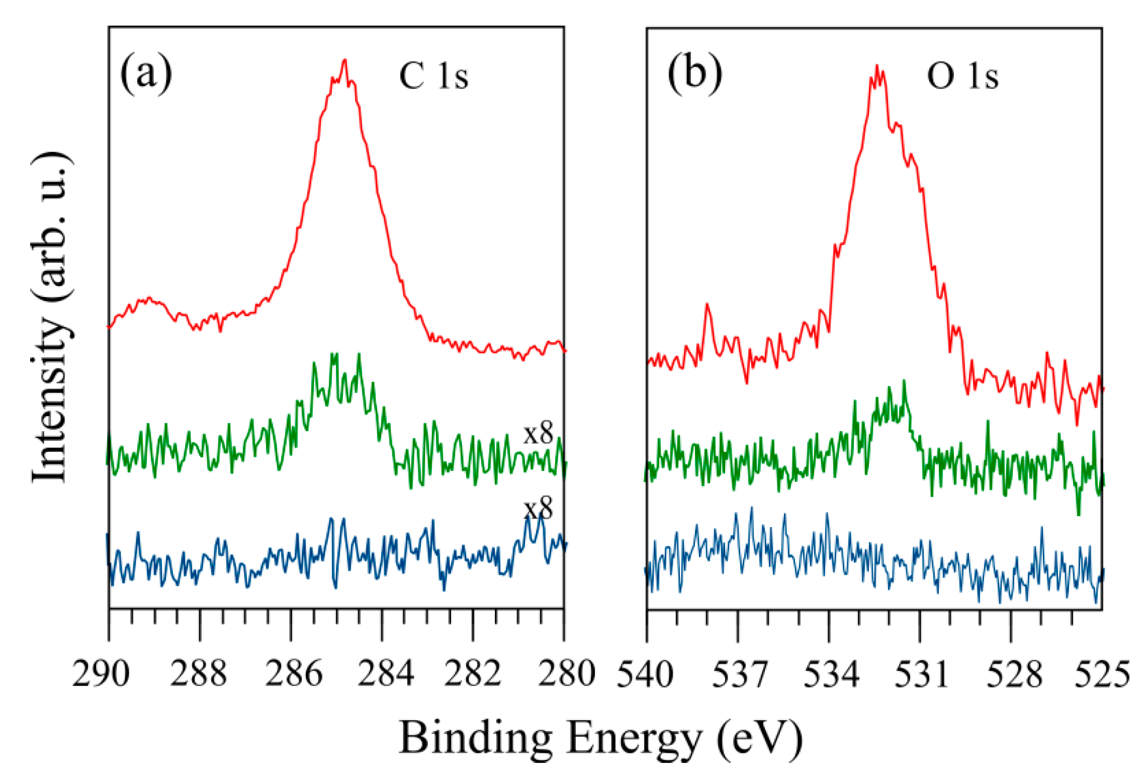
Cleaning the surface of GaN crystals under UHV is problematic because it can lead to changes in the surface stoichiometry, regardless of whether it is an ion bombardment or annealing. Ion bombardments may introduce defects and preferentially remove nitrogen atoms [62,70,71]. To eliminate this effect, the postbombardment annealing method or low-energy N-ion bombardment can be utilized [72,73,74]. The most convenient and simplest technique of surface preparation in UHV is annealing. However, during this process, the surface may also be decomposed [75]. Thus, rapid thermal annealing (RTA) should be applied. The effect of carbon and oxygen contaminant elimination by this method is shown in Figure 4. One can see that annealing in UHV may eliminate surface contamination. Two annealing cycles at 800 °C significantly reduces the signal from C and O contaminants (green lines), and six cycles lead to the achievement of a carbon- and oxygen-free GaN(0001) surface (blue lines). Unfortunately, sometimes, this method does not cause a complete elimination of contaminants, of which XPS signals remain as the middle curves in Figure 4. This is most likely dependent on the results of precleaning the sample surface by chemical treatment prior to placing it in UHV systems.
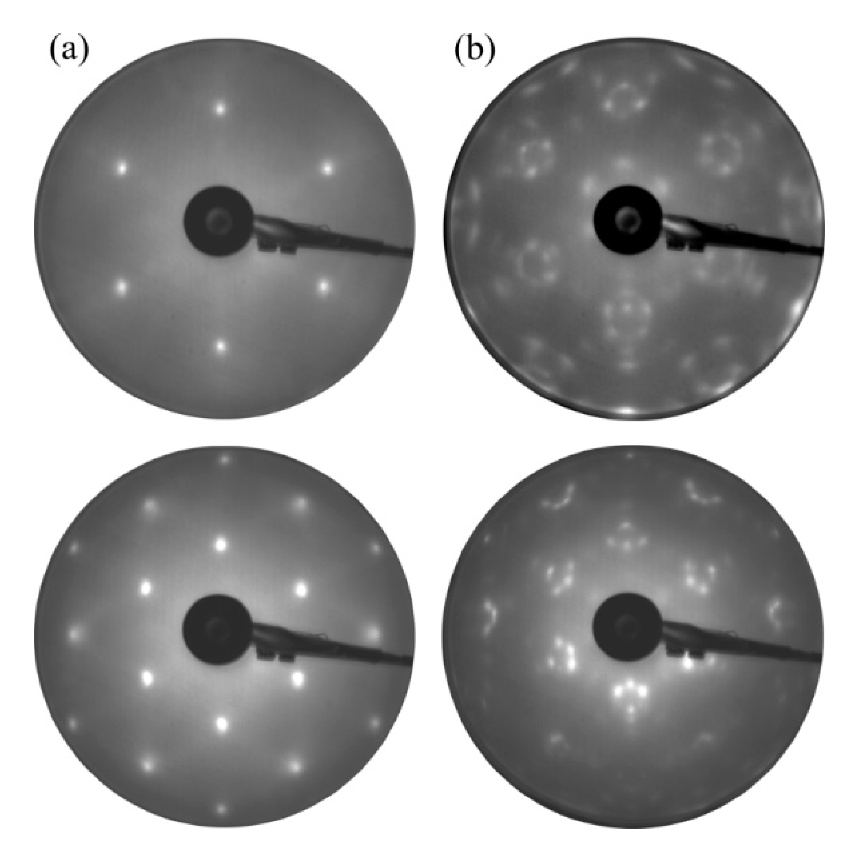
RTA can also guarantee a high-quality surface, as confirmed by LEED patterns in Figure 5a, where the strong intensity and sharp spots of GaN(0001)-(1 × 1) are visible. Several cycles of RTA may rebuild the surface, forming a facet-like terrace structure by changing the diffraction pattern [76,77]. As a result of such rebuilding, the sextets of diffraction spots appear in a hexagonal configuration around each main spot (see Figure 5b). The energy positions of the core-level line measured by XPS may vary significantly depending on the type and concentration of the dopant used in GaN. Those peak shifts do not necessarily result from the chemical properties of the surface but may only arise from different locations of the Fermi level in n-, p-, and nondoped GaN. In the perfect nondoped GaN, the EF in bulk material falls more or less in the middle of the forbidden gap; in the n-type, it is located close to the conduction band minimum, and, in the p-type, it is placed near the valance band maximum. Since photoemissions are surface-sensitive techniques, the EF position on the surface of the tested material is crucial. Due to the surface density of states (SDOSs) present on the GaN(0001), the surface Fermi level is located in a different position than in bulk material [64,78,79,80]. This means that the energy bands at the surface are bent upwards or downwards, depending on the dopant type. Figure 6 shows the distance between the valence band maximum and the surface Fermi level for Si- (n-), Mg- (p-), and nondoped GaN.
Furthermore, it indicates the difference in the EF location on the surface and in bulk. Moreover, SPV appears on GaN during XPS and UPS measurements, which results in band-bending changes [63,64]. Thus, the surface EF position relative to the VBM may also vary, depending on the magnitude of the SPV. This effect is presented below in the example of a GaN surface that is covered with native oxide and not subjected to any preparation [64]. The appointed positions of the valence band maximum of the measurements with a Kelvin probe (working in air) were compared with the VBM positions in the XPS results. Schemes of energy bands for the n-type GaN(0001) surface, in the dark (without SPV) and illuminated with UV light, were obtained, as shown in Figure 7.
On the sample in the dark, the Fermi level was located 2.7 eV above the VBM. It is a value corresponding to the higher surface density of states calculated by Segev and Van de Walle [78,79] and the position measured by Janicki and coauthors [80] for a structure with n-type doping. This value is slightly larger than the one determined by Long and Bermudez [63]. After illumination, it comes to a flattening of bands; surface photovoltage is 0.45 V. It leads to the EF location change, relative to the VBM from 2.7 to 3.15 eV. The measurement of the valence band and the Ga-3d shallow core level for the same sample is shown in Figure 8.
As can be seen above, the VBM position relative to the Fermi level falling to zero is 3.1 eV. The value is in line with the one obtained in the measurements with a Kelvin probe for the illuminated sample. The outcomes for p-GaN(0001) covered with native oxide also showed that the EF level for the sample in the dark is located 1.75 eV above the valence band maximum and corresponds to lower SDOS, as calculated by Segev and Van de Walle, and the value measured by Janicki for a sample with p-type doping. After illuminating the p-GaN(0001) surface with UV photons, the energetic bands flatten and the EF level locates 1.2 eV above the VBM. The same value was obtained with XPS measurements; therefore, when the surface is irradiated with X-rays, the SVP voltage is the same as the one obtained with UV light illumination (−0.55 V) [64].
The results presented in [64,80] show the bistability of the Fermi level. It should be noted that although the energies of the Fermi levels measured on the surface are practically the same as in the theoretical calculations [78,79], the nature of SDOS found experimentally differs from the calculated one. The existence of lower SDOS in the calculations is related to the (2 × 2)-GaT4 reconstruction—such reconstruction would not survive on an oxidized surface or on nondoped GaN/doped GaN samples used in Janicki’s work phase boundaries [80].
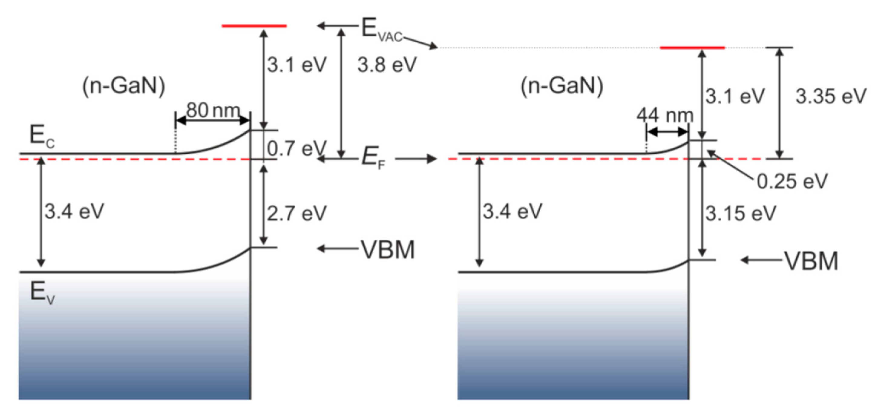
As mentioned before, surface preparation is a very important stage in the process of formation of an electronic device. Cleaning through bombardment, which is usually carried out using high energy (1–10 or even 10–500 keV), can cause large changes in the structure morphology. Therefore, in order to counteract the changes in GaN surface properties and its degradation, less-invasive cleaning processes are needed. In [73,74], a process of bombardment with nitrogen ions, with a relatively low energy level of 200 eV, was proposed. This solution enables the cleaning of the surface by sputtering, yet is much less destructive and also compensates for nitrogen loss from the near-surface region. During the bombardment, the nitrogen is partly implanted. The study shows the impact of N-ion bombardment of the n-GaN(0001) surface on its physicochemical changes [73]. As a result of the surface bombardment, there is a change in the UPS spectrum, as shown in Figure 9.
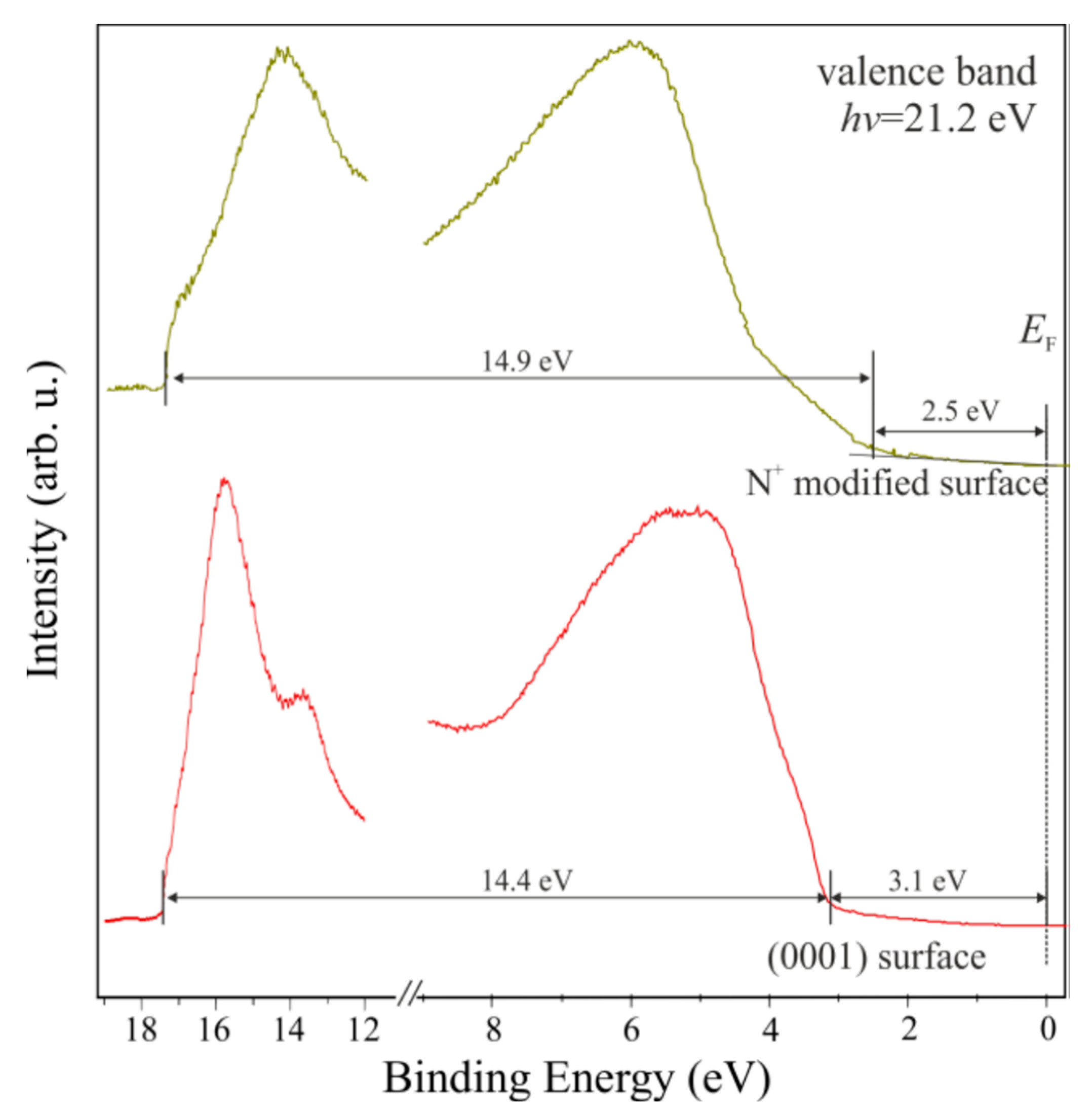
After bombardment, the valence band maximum shifts towards lower binding energies, from 3.1 to 2.5 eV. The same happens with the Ga-3d and N-1s core level lines; they also shift towards lower binding energies. The influence of bombardment on the electronic structure is schematically presented in Figure 10. Despite the process of bombardment being effectuated at relatively low energy, the receiving GaN surface is not orderly—there are no diffraction images.
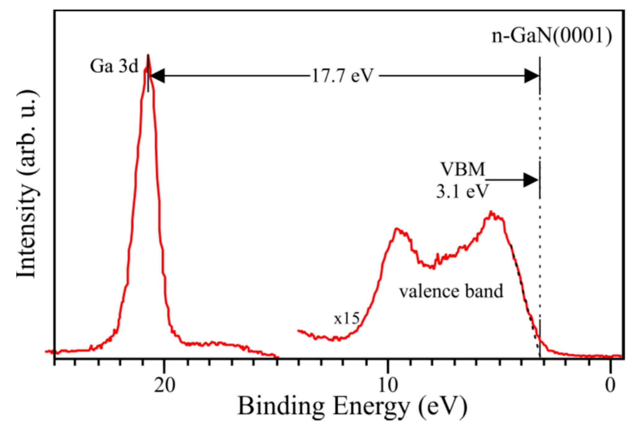
In the case of a p-type surface, bombardment with N ions also leads to changes [74]. However, in this case, the bands bend even more. The EF level is in the same position as on the bombarded n-GaN surface, i.e., 2.5 eV above the VBM. The Ga-3d and N-1s core level lines behave similarly. It can be reasoned that as an effect of bombardment, there is an inversion of carrier occupation in the subsurface layer, and the surface shows an n-type feature. Interestingly, after a short annealing of a bombarded p-GaN surface, there is a splitting of the Ga-3d and N-1s peaks. Two curves are also observed in the valence band spectrum—its top edge has two slopes. The results are shown in Figure 11. The components A, B, which are included in the Ga-3d spectrum, are located around 17.7 eV below the two edges of the valence band, which are separated by 1.5 eV. The same value separates the components included in the N-1s line. This suggests the emergence of two regions on the surface that are electrically separated—one with n-type properties, the other with p-type properties.
It is worth noting that bombardment with nitrogen ions leads to changes in the band bending of both the n-GaN and p-GaN samples; the Fermi level is located 2.5 eV above the VBM, which is in line with the result obtained by Long and Bermudez [63]. Such a result may be an effect of a decrease in the influence of the SPV voltage on both surfaces, as well as the introduction of donor states on the p-GaN surface, causing the EF pinning at higher SDOS, deriving from gallium dangling bonds.
Therefore, the dispersion in Fermi level placement in relation to the valence band maximum in photoemission experiments, which is also observed in the author’s publications, can be caused by a different condition of the GaN surface—different concentrations of donor and acceptor states on the surface, in subsurface layers, and in the bulk samples used. Moreover, surface quality and the number of defects can also have an influence on the magnitude of surface photovoltage. To determine whether the peak shift is caused by a chemical reaction or not, its location relative to the VMB needs to be known. As shown above, on the GaN(0001) surface, the Ga-3d state is located around 17.7 eV above the VBM. There are also different values of the ∆E in the literature, with a spread of ±0.3 eV from the value indicated here.
3.2. Mn on GaN(0001)
Manganese belongs to the transition metals in group VII on the periodic table. The element exhibits poor electrical and thermal conductivity properties. Manganese has a density of 7.2 g/cm3, its thermal conductivity is 7 W/(m∙°C), and its electrical resistivity amounts to 1.6 × 10⁻⁶ Ω∙m (at RT). It melts at 1246 °C, and its boiling point is 2061 °C (under standard pressure). Mn needs a high temperature to be evaporated in a vacuum and, at 930 °C, has a vapor pressure of 10−8 mbar. Manganese has a multifaceted field of industrial uses, from metallurgy, particularly in stainless steels, to electronic applications.
Surface techniques have been used to measure the interfacial behavior of Mn and GaN in the context of the possible formation of diluted magnetic semiconductor layers. The studies were inspired by the spintronic potential of MnGaN alloys [12,13,14]. Thin films of Mn on GaN have mainly been reported for the (000) N-terminated surfaces [18,19,20,81,82,83]. These works generally refer to structural analysis for ultra-thin coverage. One exception to this is [20], where the interaction of Mn with GaN(000) was investigated by photoemission experiments with synchrotron radiation. The results of Mn thin-films on GaN(0001) surfaces, concerning structural characterization by STM, were reported in [15,16,17], whereas the physicochemical properties of Mn on GaN(0001) were studied by the author using XPS and UPS with nonmonochromatic excitation sources in [22,23,24].
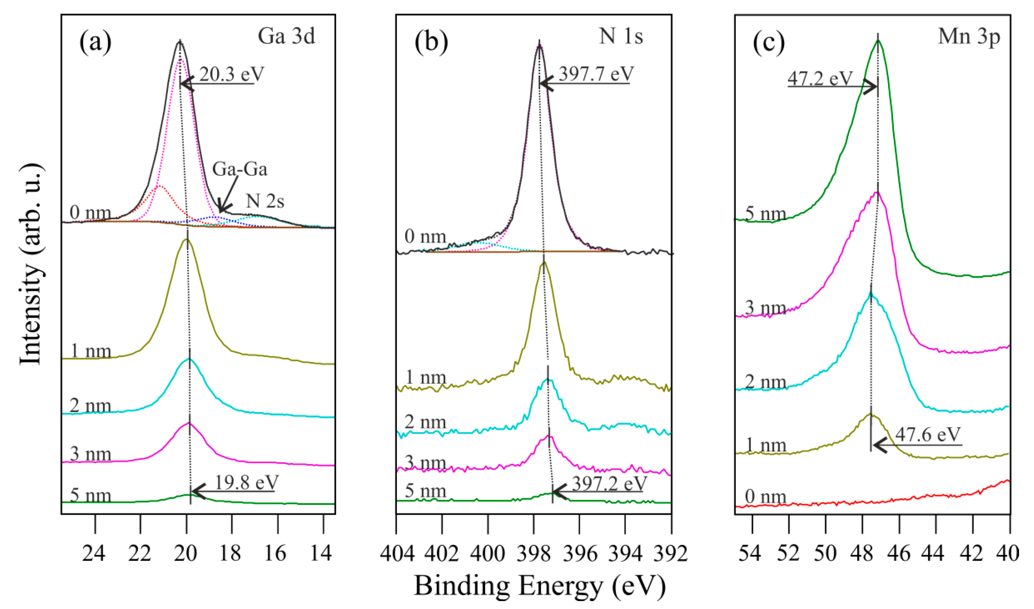
Early stages of coating the nondoped GaN(0001) surface with Mn films and the influence of annealing on system properties have been described in [22,23]. The growth of Mn film by PVD and characterization were performed in situ on MOCVD GaN(0001). The initial bare surface that was prepared by RTA exhibited the (1 × 1) structure (confirmed by LEED, similar to that in Figure 5a) and had a trace amount of oxygen. In these works, the Mn films formed at RT gave no diffraction patterns, indicating that they are amorphous. The changes in the Ga-3d, N-1s, and Mn-2p core level lines with a thickness of deposited Mn film are shown in Figure 12. The peaks of the bare surface contained the same components, as already presented in Figure 3. Namely, the subpeaks for the Ga-3d are from the Ga–N, Ga–O, and Ga–Ga bonding and the N-2s state. The subpeaks for N-1s originate from the N–Ga and N–H bonds. One can see that the substrate XPS lines shift towards a lower BE after the deposition of Mn films. The Mn-3p peak behaves in the same manner.
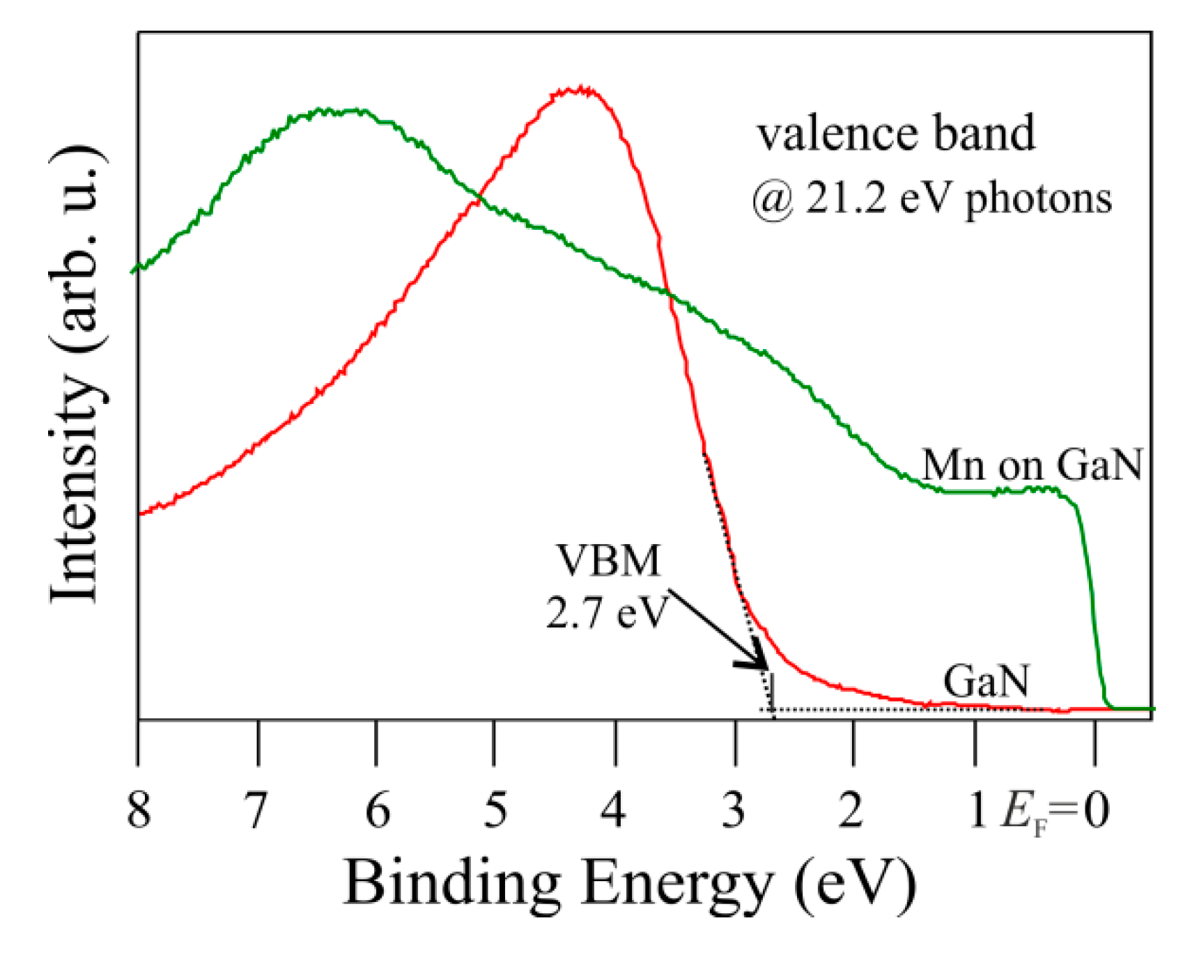
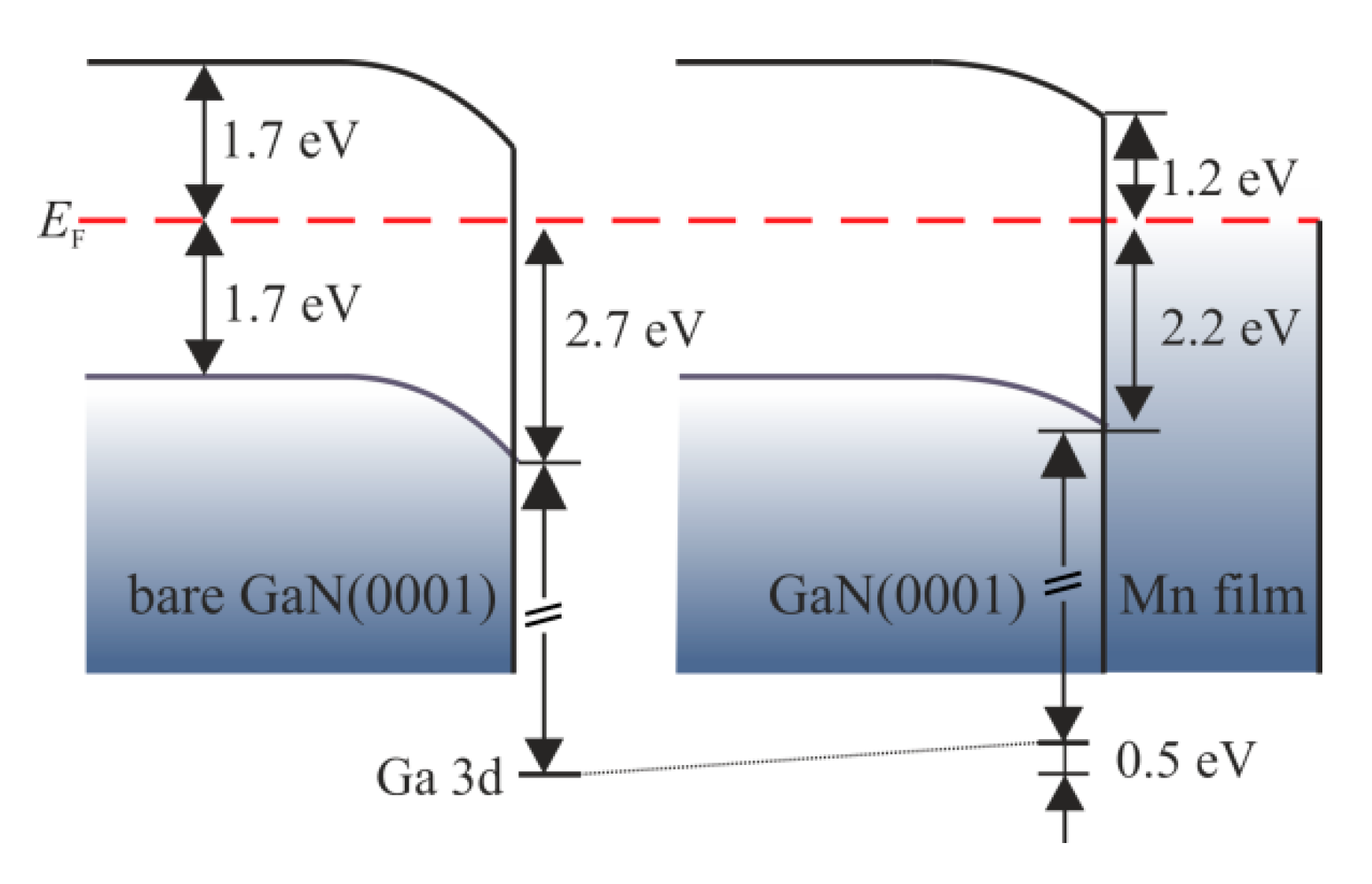
The peak shifts are a result of charge transfer through the Mn/GaN phase boundary and not a chemical reaction of Mn with GaN. Mn films do not behave like those deposited on the (000-1) surface [20]. The electron transfer at the interface causes the formation of the Schottky barrier, the height of which (SBH) can be simply calculated from the formula: , where Eg = 3.4 eV is the bandgap of GaN, and is the position of VBM at the interface after Mn deposition. The latter value cannot be obtained directly from UPS measurements since GaN is coated with Mn, which introduces a new electron density of state (DOS). This means that the VB of GaN is no longer visible, as presented in Figure 13. However, the VBM for thin-film-covered GaN can be determined indirectly from the Ga-3d peak shift due to the energy distance between Ga-3d and the VBM being constant: . This procedure was previously applied to metal films on SiC [84,85]. In Figure 14, the energy level diagrams of the bare GaN(0001) and Mn/GaN(0001) interface with the SBH are constructed based on the UPS and XPS data.
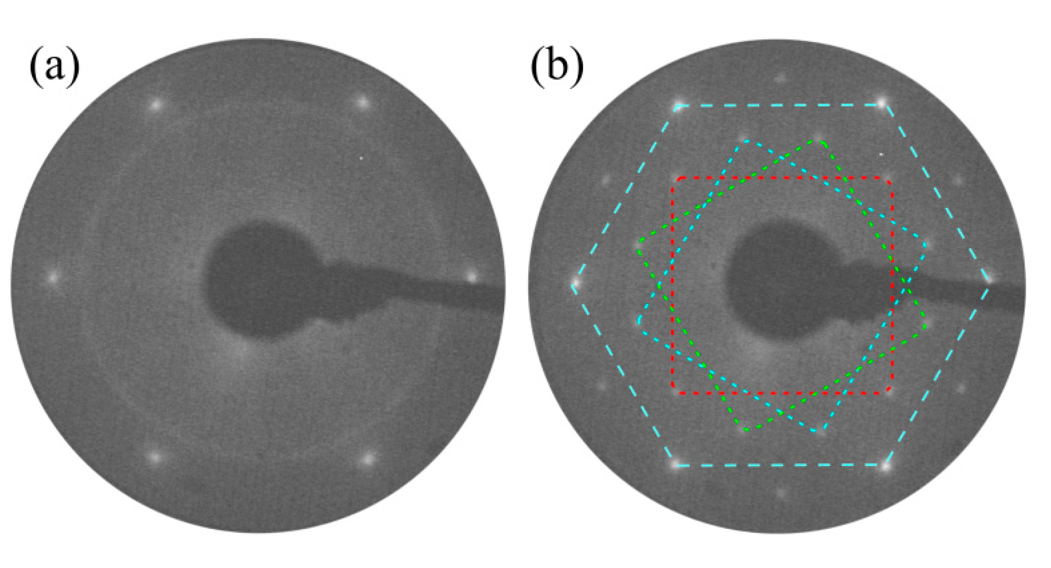
Annealing of the Mn films on GaN(0001) in UHV is interesting from the aspect of Mn-diluted GaN semiconductor formation. The dissolution of Mn atoms in bulk GaN(000-1), induced by thermal treatment, was observed using STM [18] and secondary ion mass spectrometry (SIMS) [86]. (Mn)GaN films obtained that way show ferromagnetic behavior [87]. Experiments examining the changes in physicochemical properties of the films on GaN(0001) crystals under the influence of annealing were presented in the author’s works [23,24]. In [23], the Mn-film-covered nondoped GaN(0001) was annealed at 500 °C, followed by 800 °C for 3 min for each temperature. The process strongly modified the morphology of the system. The Mn films on GaN(0001), which are amorphous, crystallize after annealing at 500 °C. LEED patterns for this stage reveal diffraction rings, as shown in Figure 15a. They come from randomly oriented rotational domains of (2.3 × 2.3) structure in relation to the substrate, giving a lattice parameter equal to 7.3 Å. This value matches the α-Mn(111), for which the surface lattice constant is from 7.39 to 7.68 Å [88]. The small transformation of the lattice can be attributed to Ga incorporation into the Mn structure. After annealing at 800 °C, the thin film alters into a well-ordered MnGa surface alloy. The LEED pattern in Figure 15b exhibits three sets of (1.21 × 1.21) squareR15 structures coming from the film, with a lattice constant equal to 3.86 Å. They are rotated at 60° relative to each other. The achieved lattice parameter is in line with the structure of the single-phase Mn1+xGa (0 < x < 1) alloys for which the lattice constant is around 3.88 Å [89], clearly demonstrating the formation of alloys on the surface.
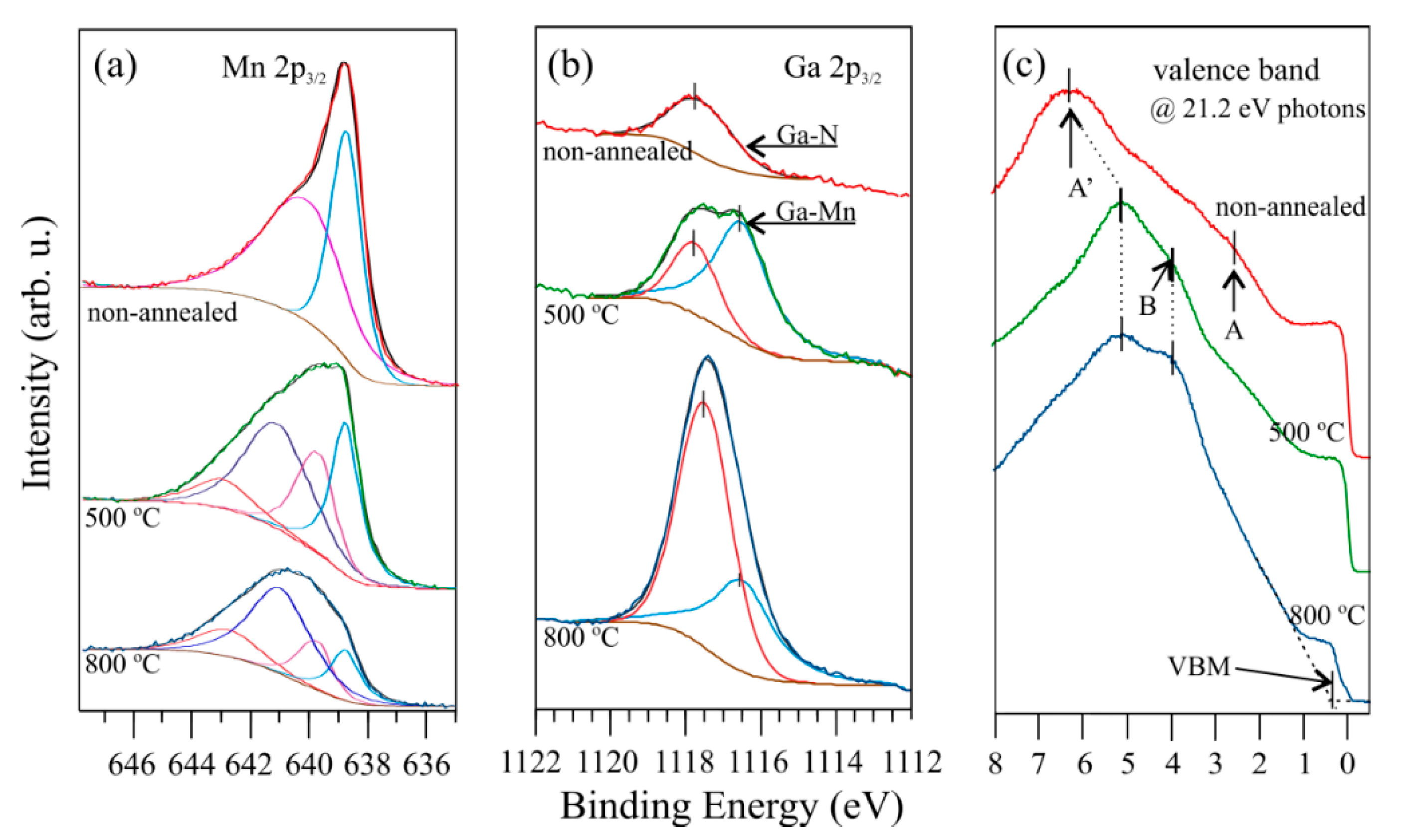
XPS and UPS provide information on the physicochemical properties of the annealed system. The changes in the Mn-2p doublet introduced by thermal treatment are presented in Figure 16a. The analysis of the Mn-2p3/2 peak for the nonannealed system shows that it can be fitted by two subpeaks, with BEs of 368.7 and 639.75 eV. Annealing means that the Mn-23/2 becomes broader, and to reproduce its shape, other components need to be added, with BEs of 641 and 642.85 eV. Figure 16b shows that the Ga-2p3/2 peak can be fitted by one or two subpeaks for the non- and annealed system, respectively. They are located at 1117.6 and 1116.5 eV. The subpeak at a lower BE, in the case of the bare GaN(0001) surface, corresponds more or less to the Ga–Ga bonding, but on the annealed Mn-covered GaN surface, it should be attributed to the Mn–Ga bond, which has a metallic character with a very weak chemical shift [90]. The subpeak intensities for both the Mn-2p3/2 and Ga-2p3/2 states depend on the annealing temperature. The changes to both the core level lines, appearing during annealing, are the result of atom exchange at the phase boundary. There are two processes, i.e., some manganese atoms diffuse into the substrate, substituting gallium elements at a subsurface region. In turn, these release Ga atoms directly to the Mn-film-covered surface. These processes result in the formation of (i) the (Mn)GaN-like alloy, which is demonstrated by the two extra subpeaks in Figure 16a (Curves 2 and 3 from the top) [21,91] and was already reported in other works [18,86]; (ii) the Mn–Ga surface alloy, manifested by the second component in Figure 16b (Curves 2 and 3). This surface alloying—the intermixing of Ga atoms with the thin film on the GaN(0001) surface—is also observed in the case of Ni and Pd adsorbates [29,34].
Knowing that Mn is dissolved in the substrate, it is interesting how the VB is modified under the influence of annealing. This information was provided by UPS measurements, as shown in Figure 16c. The shape of the VB of Mn-film-covered GaN, annealed at 500 °C, is changed—the feature marked as A disappears, the maximum A′ is shifted towards a low BE, and another feature marked with B emerges. Despite the above changes, electron DOS in the vicinity of the EF is still high, demonstrating a metallic character of the adlayers. Annealing at higher temperature enhances the modification—the feature intensity of A′ decreased and that of B increased. The Fermi edge is still visible, but its intensity is definitely lower. Moreover, it can be seen that the VB of the Mn-doped GaN(0001) shifts towards a lower BE, and the VBM is 0.4 eV below the EF. This result is very interesting, especially for p-GaN crystals, for which the surface Fermi level is far away from the VBM due to band bending at the surface. This leads to a problem with obtaining Ohmic contacts with this material, as was noted in [92]. The potential to modify the VB of GaN by dissolving Mn thermal initiation was applied to p-GaN(0001) in [24]. By annealing the Mn-film-covered p-GaN under UHV conditions, Mn was dissolved in the subsurface layer of the p-GaN, similar to what was described above in the case of nondoped GaN. Then, in order to remove the MnGa alloy from the surface, for which UPS showed metallic properties, the system was annealed at 900 °C. After that, the obtained surface was free of the adlayer with the metallic character. However, as a result of high temperature, the obtained surface was faceted. The consequence of such a process is visible in the LEED patterns as extra spots [24], comparable to those presented in Figure 5b.
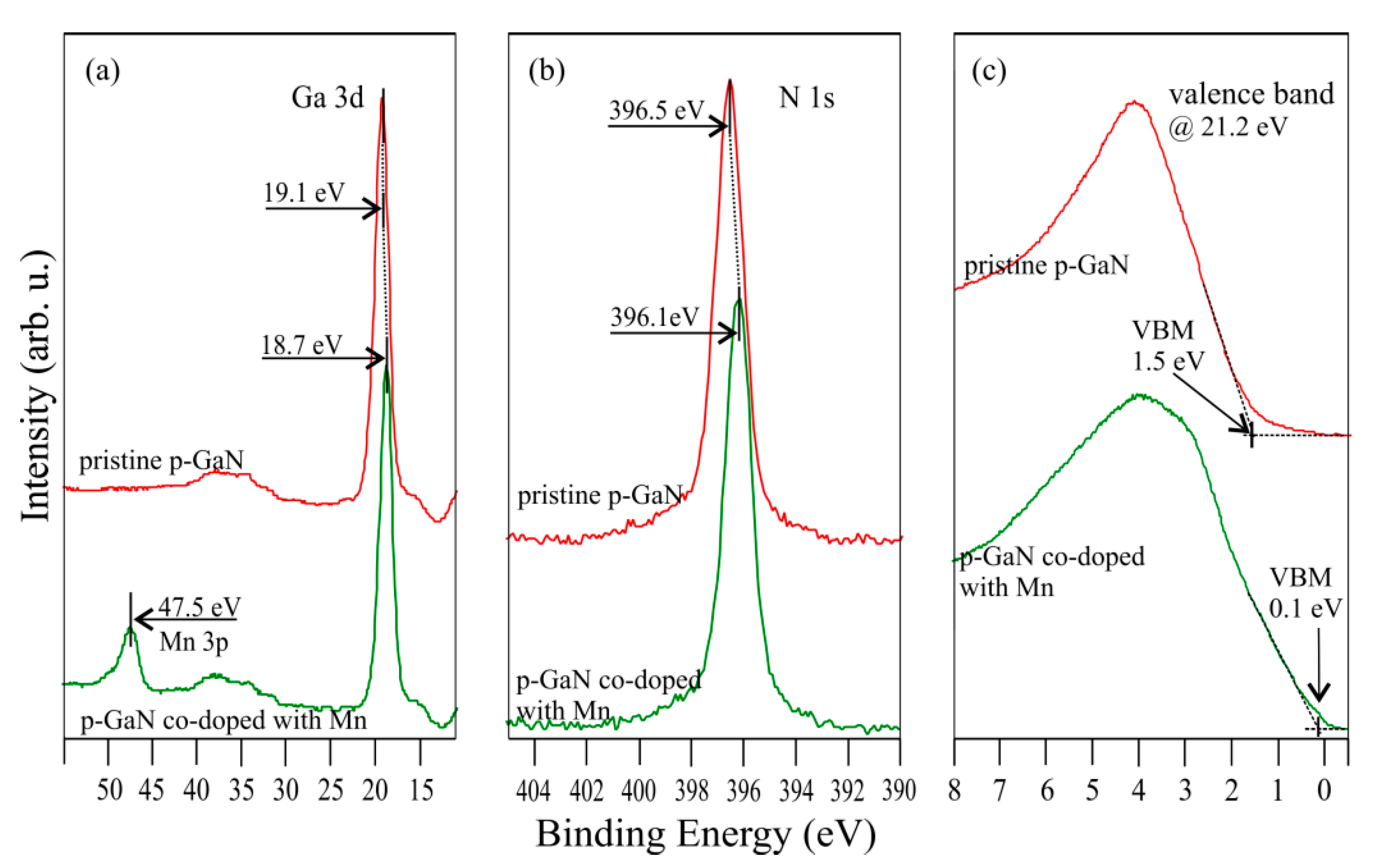
XPS and UPS results of the research of [24] are presented in Figure 17, which shows changes in the Ga-3d and N-1s core level lines caused by the incorporation of manganese. Ga-3d is located at 19.1 and 18.7 eV, before and after the Mn incorporation, respectively. Apart from the Ga-3d state, the Mn-3p peak at 47.5 eV is present on the p-GaN Mn codoped material, as shown in Figure 17a. The N-1s peak shifts towards a lower BE by 0.4 eV to the position of 396.1 eV after the Mn atoms’ introduction. Hence, the shifts of Ga-3d and N-1s are the same; a similar observation was also noted in another paper [93], where Mn implantation by an ion bombardment was applied.
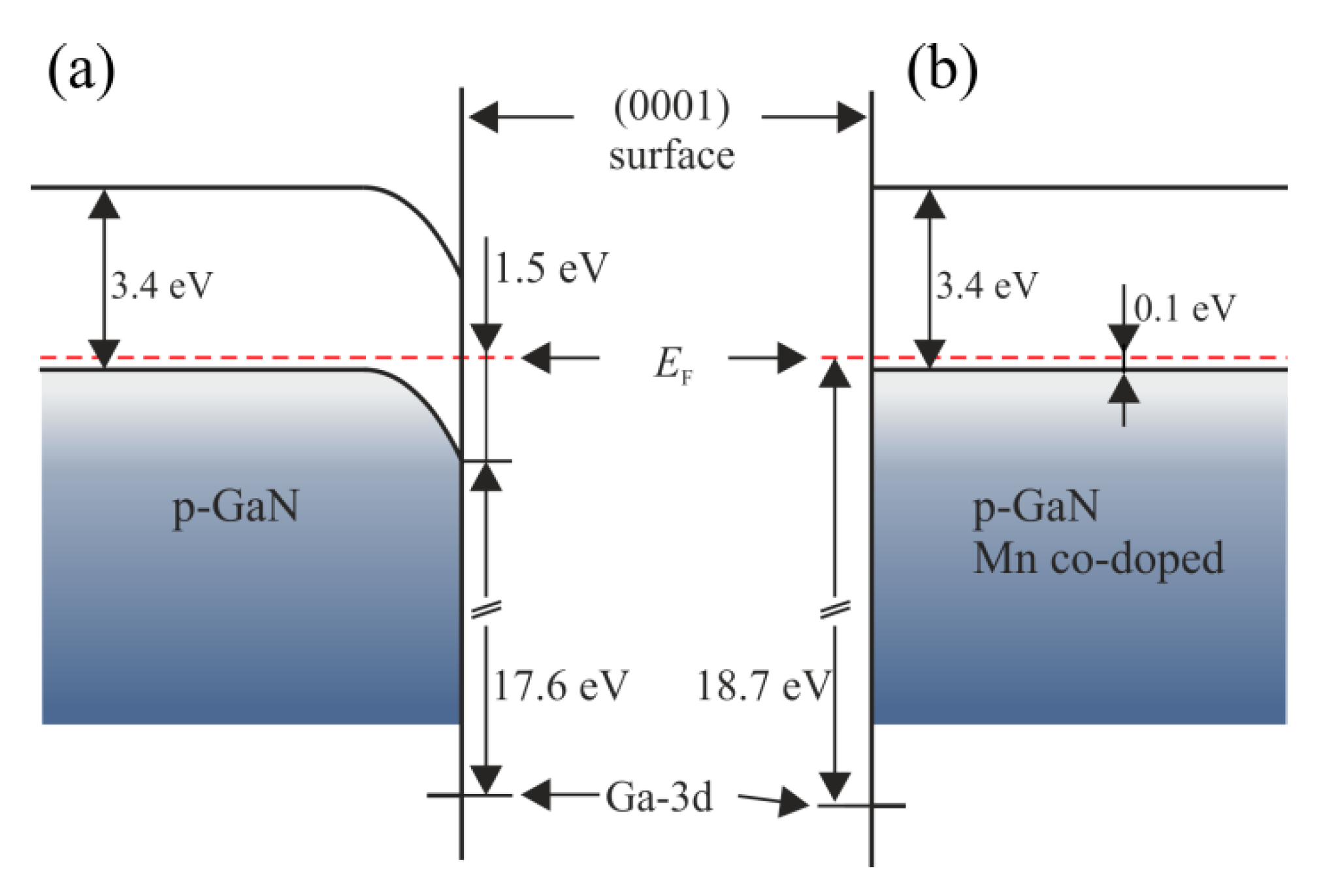
The presence of Mn atoms in p-GaN has a strong impact on the VB, and the effects are especially visible near the Fermi level. The VBM is 1.5 and 0.1 eV below the EF for the bare p-GaN(0001) surface and the p-GaN Mn codoped material, as shown in Figure 17c. The VB of the Mn-incorporated p-type GaN varies significantly, the electron DOS begins almost at the Fermi level, and its shape is very similar to that for nondoped (Mn)GaN-like alloy, not included at the edge of the Fermi, as presented in Figure 16c. The widening of the VB in the vicinity of the Fermi level follows from the subsurface layer’s modification caused by the incorporation of Mn atoms, leading to the formation of a p-type (Mn)GaN-like alloy. This is in line with the literature [94,95,96], where it is shown that the Mn presence in the GaN matrix reconstructs the VB. Another reason that the VBM is practically located at the Fermi level may be surface-state deprivation and, thus, an elimination of band bending on GaN(0001). The band energy diagrams constructed based on the UPS and XPS data for bare p-GaN(0001) and p-GaN(0001) codoped with manganese are shown in Figure 18. There is a clearly noticeable flattening of the band on the surface of the p-GaN Mn codoped material, with the assumption that the bandgap does not change.
3.3. Ni and Pd on GaN(0001)
Nickel and palladium are transition metals in group VIII on the periodic table. Both elements exhibit good electrical and thermal conductivity properties. Nickel and palladium have a density of 8.9 and 12.9 g/cm3, respectively. Their thermal conductivities are 91 and 71 W/(m∙°C). The electrical resistivity of Ni is 69 × 10−9 Ω∙m, and of Pd, 105 × 10−9 Ω∙m (at RT). Ni melts at 1455 °C, and its boiling point is 2730 °C (under standard pressure). Pd melts at 1555 °C, and its boiling point is to 2963 °C. Ni and Pd need a high temperature to be evaporated in a vacuum. Ni at 930 °C and Pd at 842 °C sublimate with a vapor pressure of 10−8 mbar.
Nickel is used for metal contacts with GaN. It can be applied as a single element layer or a multilayer with other elements, mainly from the nickel family, gold, and silver [26,27,28,31]. Structural and topographical analysis of Ni on GaN performed by STM was reported in [97,98]. The former work concerns the growth mode and interfacial compound formation. The latter focuses on topographic differences between Ni layers deposited at RT, followed by annealing at 650 °C, and Ni layers deposited on the substrate at 650 °C; this results in the surface consisting mainly of Ni3Ga. The latter procedure gives more strongly dispersed films and is better for catalytic converters, where Ni–Ga alloys can be applied [35,36]. Photoemission experiments were carried out to measure the surface condition effects on the properties of obtained contacts to GaN and the temperature impact on the electronic properties of Ni/GaN interfaces [99,100]. In [25], the physicochemical properties of Ni on GaN were investigated with the XPS technique. It was shown that a disordered Ni film grows continuously, in a layer-by-layer manner (Frank van der Merwe mode), and the chemical interaction between the adsorbate and the substrate can occur even near RT.
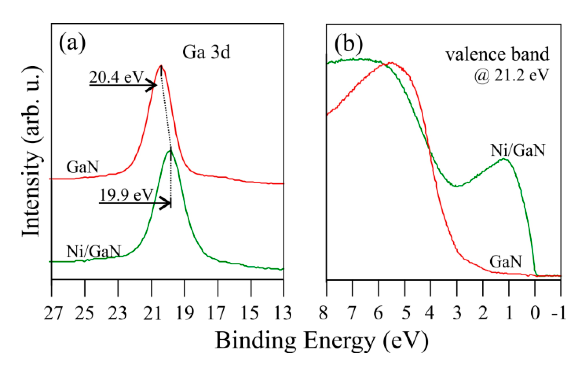
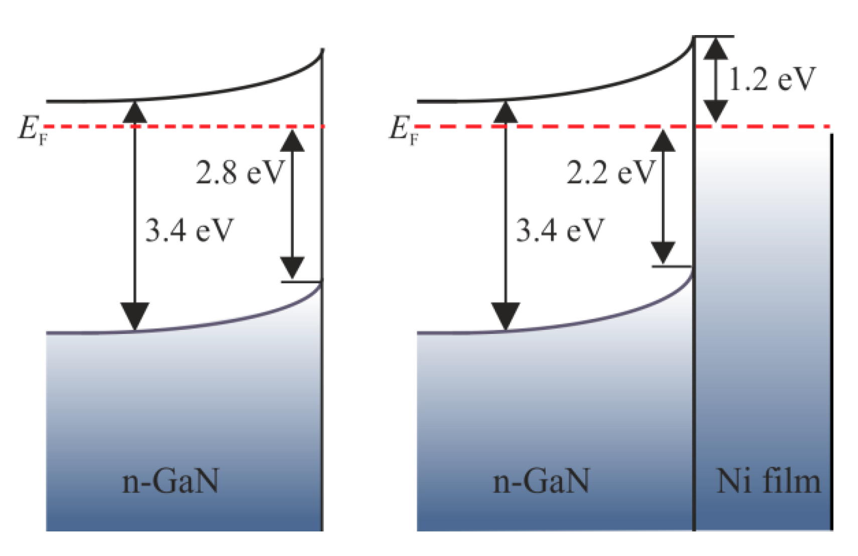
The morphology of Ni-film-covered GaN(0001) and the morphological changes introduced by annealing, as well as the SPV impact on the XPS and UPS results, were presented in the author’s papers [29,30]. In these studies, the growth of Ni film by PVD and its characterization were performed in situ on n- and p-type MOCVD GaN(0001) samples. Spectroscopic data were obtained with nonmonochromatic excitation lines. The bare surfaces prepared by RTA under UHV conditions had only small amounts of carbon and oxygen contamination and revealed the (1 × 1) structure (confirmed by LEED, similar to that in Figure 5a). In these works, the Ni films formed at RT exhibited no diffraction pattern, indicating that they are amorphous. After deposition of Ni film on the bare n-type GaN(0001) surface, the Ga-3d core level line shifts towards a lower BE by 0.5 eV to the position 19.9 eV, as shown in Figure 19a. The shift is caused by the Schottky barrier formation. The valence band of the bare and Ni-film-covered GaN is presented in Figure 19b. It is clearly visible here that the VBM for bare GaN(0001) is 2.8 eV, so for the initial surface, it is above the Ga-3d line by ∆E = Ga-3d − VBM = 17.6 eV. After Ni deposition, the Fermi edge is distinctly prominent; in the spectrum is the characteristic maximum, with a BE equal to 1.2 eV. The SBH can be simply calculated by the same procedure as applied to Mn films on GaN (see Section 3.2) as well as to Pd films on GaN [101].
The formula is , and the position of =2.2 eV, which gives SBH = 1.2 eV. The obtained value is consistent with the literature, where the SBH is in the range of 0.95 to 1.4 eV. The energy level diagrams of bare and Ni-film-covered GaN(0001), with the SBH constructed based on the UPS and XPS data, are shown in Figure 20.
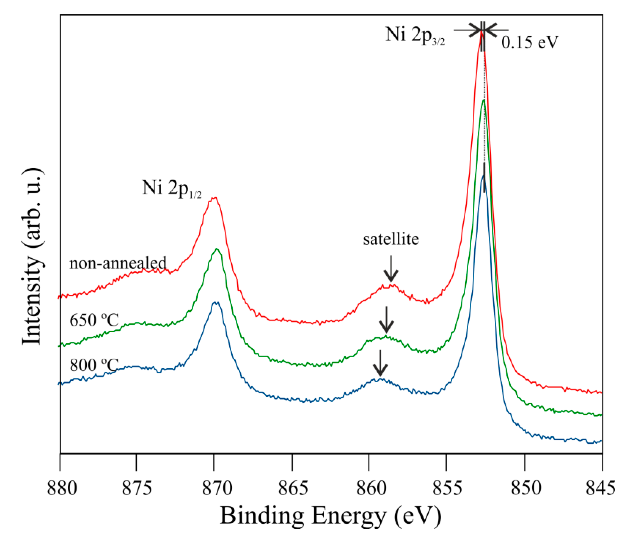
The annealing of Ni films on GaN(0001) is interesting from a basic point of view to gain a deep insight into the processes occurring on the interface since this stage is often used in contact creation technology. Temperature treatment of the system by subsequent annealing at 650 °C and then 800 °C leads to a slight shift of the Ni-2p doublet towards a lower BE by 0.15 eV, reaching 870.25 and 853.05 eV for the Ni-2p1/2 and Ni-2p2/3, respectively. The position of the shake-up satellite changes, allowing us to monitor Ga–Ni intermixing phases at the surface. The satellite positions are 5.8, 6.2, and 6.7 eV, below the parent peak for the non- and annealed surfaces at 650 °C, followed by 800 °C, respectively (visible in Figure 21). These relative positions of the satellite are characteristic of Ni3Ga and NiGa or Ni3Ga2 alloys, respectively [102,103]. This does not imply that only these phases of Ga–Ni alloys are presented in the film formed after annealing. It is, with a high probability, not a homogeneous film and consists of different phases of alloys and metallic nickel. The results indicate the dominant phases in the film.
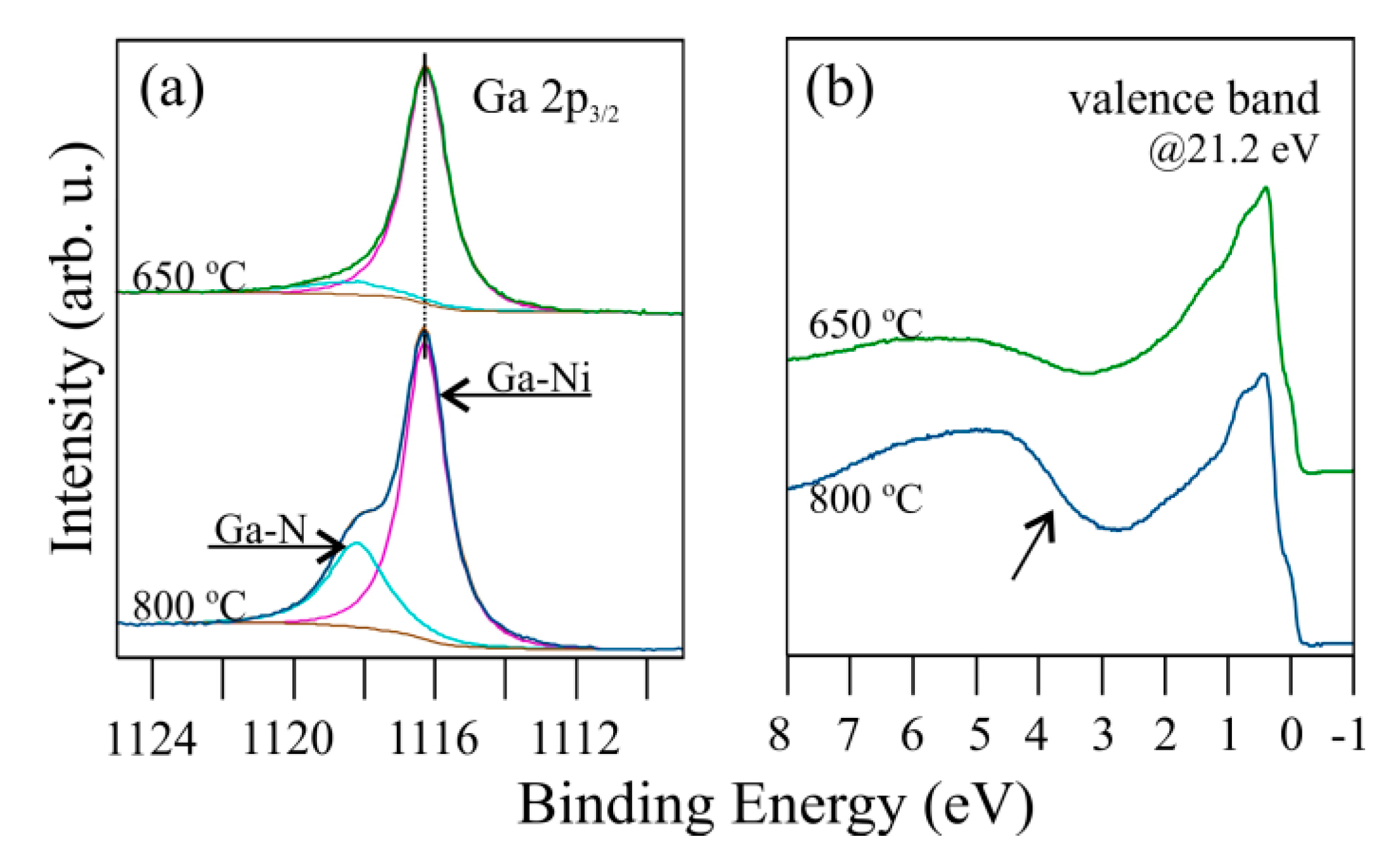
Mixing Ni with Ga will result in the latter atoms diffusing from the GaN subsurface layer into the adsorbed Ni film. The result of the intermixing of these two atoms is presented in Figure 22a. The Ga-2p3/2 peak splits into two subpeaks. The subpeaks at BEs at 1118.3 and 1116.3 eV are attributed to Ga–N and Ga–Ni bonding. Further annealing at a higher temperature leads to a change in the intensity of the components. The Ga–N bond becomes more visible, indicating that the surface of the substrate is being partially uncovered. Ni atoms are not included in the subsurface layers of GaN, and a substitutional alloy is not formed. The system behaves differently from Mn films on GaN, and the mixing appears only on the surface. In addition to temperature-induced changes in core level lines, the alterations also appear in the valence band, as shown in Figure 22b. The spectrum is strongly modified in comparison to the system not annealed. In the vicinity of EF are two features at 0.6 and 0.9 eV. The DOSs near the Fermi level for the sample, after annealing at both temperatures, are very similar. It is worth noting that for the system annealed at 800 °C, the VB of the substrate became visible (marked by an arrow in Figure 22b), which is in line with the changes to the Ga-2p3/2 peak. The Fermi edge is similar to that obtained by XPS in [103], which is characteristic of a Ni3Ga alloy. Therefore, UPS measurements only show one phase of the Ni–Ga alloy, regardless of annealing temperature (unlike XPS measurements of the Ni-2p line). Due to the fact that UPS is more surface-sensitive than XPS, the results show that the Ni3Ga alloy is the most dominant phase on the top of the system’s surface.
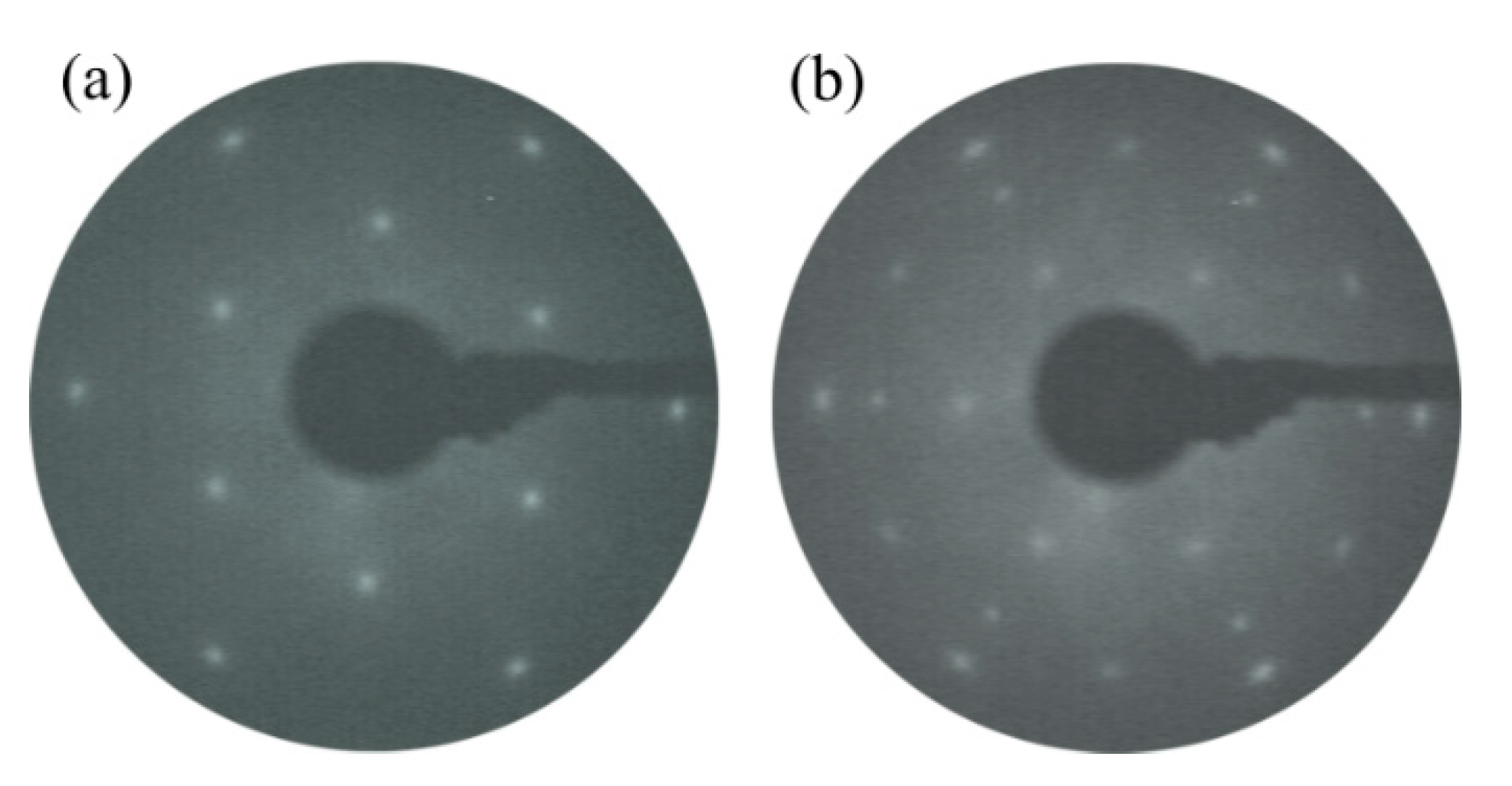
Reconstruction on the surface after annealing is presented in Figure 23. LEED patterns from Ni film annealed at 650 °C show strong, sharp spots corresponding to the Ni(111)‑(√3 × √3)R30° structure, with a lattice constant of 2.58 Å, and, after annealing at 800 °C, reveal sharp diffraction spots of the Ni(111)-(2 × 2) and GaN(0001)-(1 × 1) structures. The presence of spots corresponding to GaN(0001)-(1 × 1) shows that further Ni–Ga alloying is accompanied by coalescence and, consequently, the partial opening of the film and the uncovering of the substrate surface, which is consistent with spectroscopic observations.
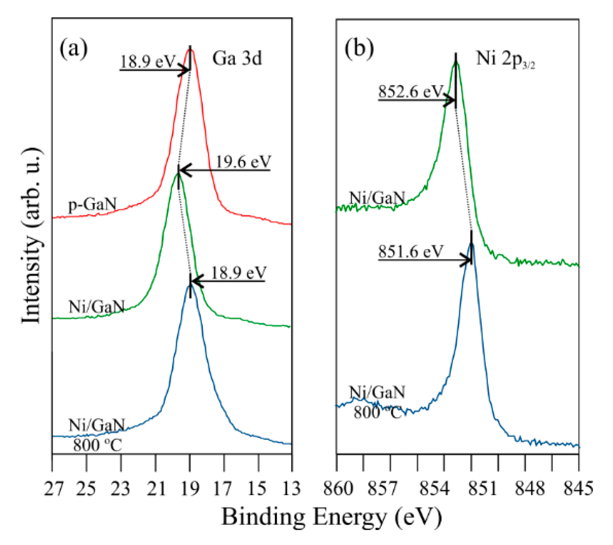
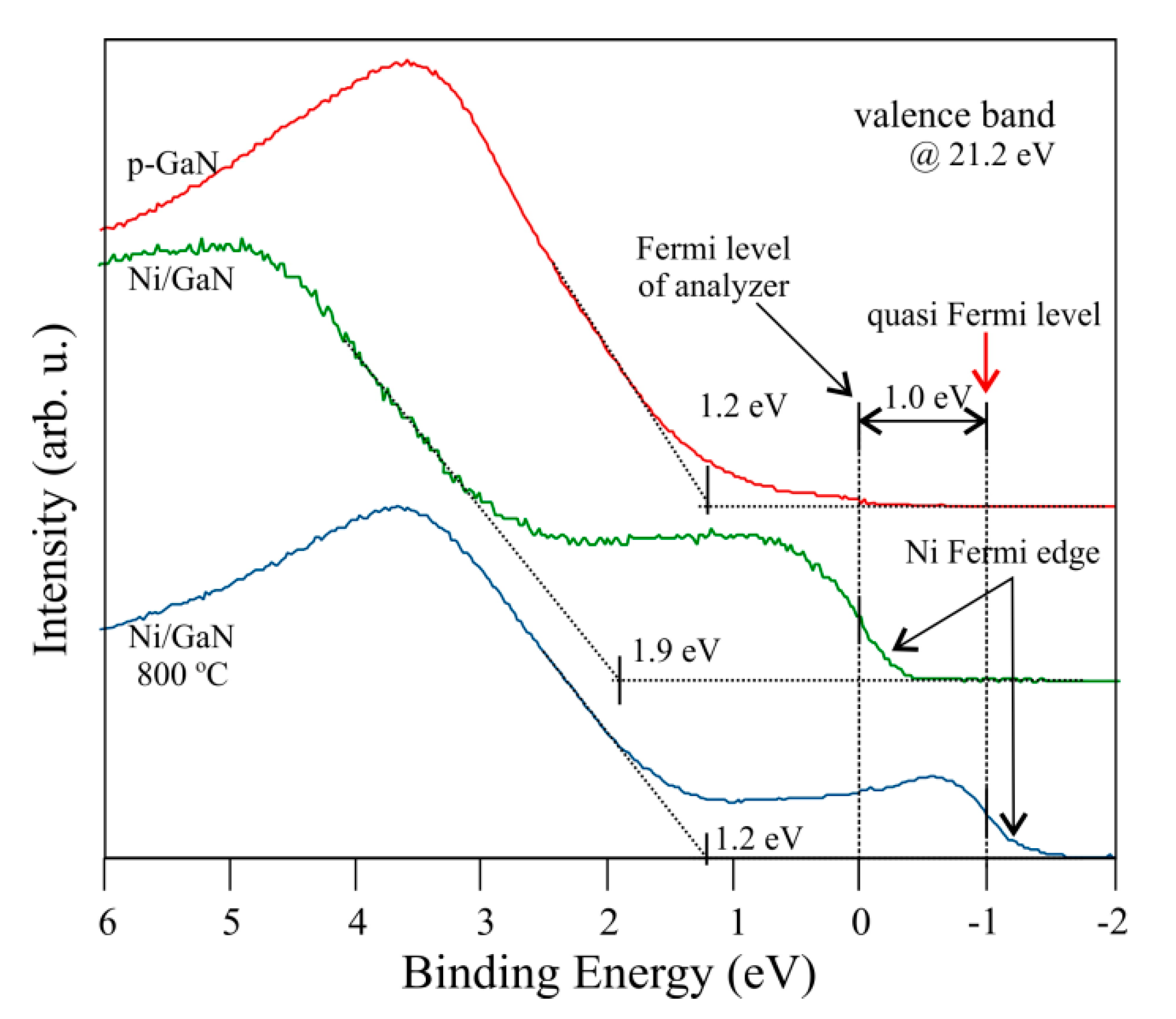
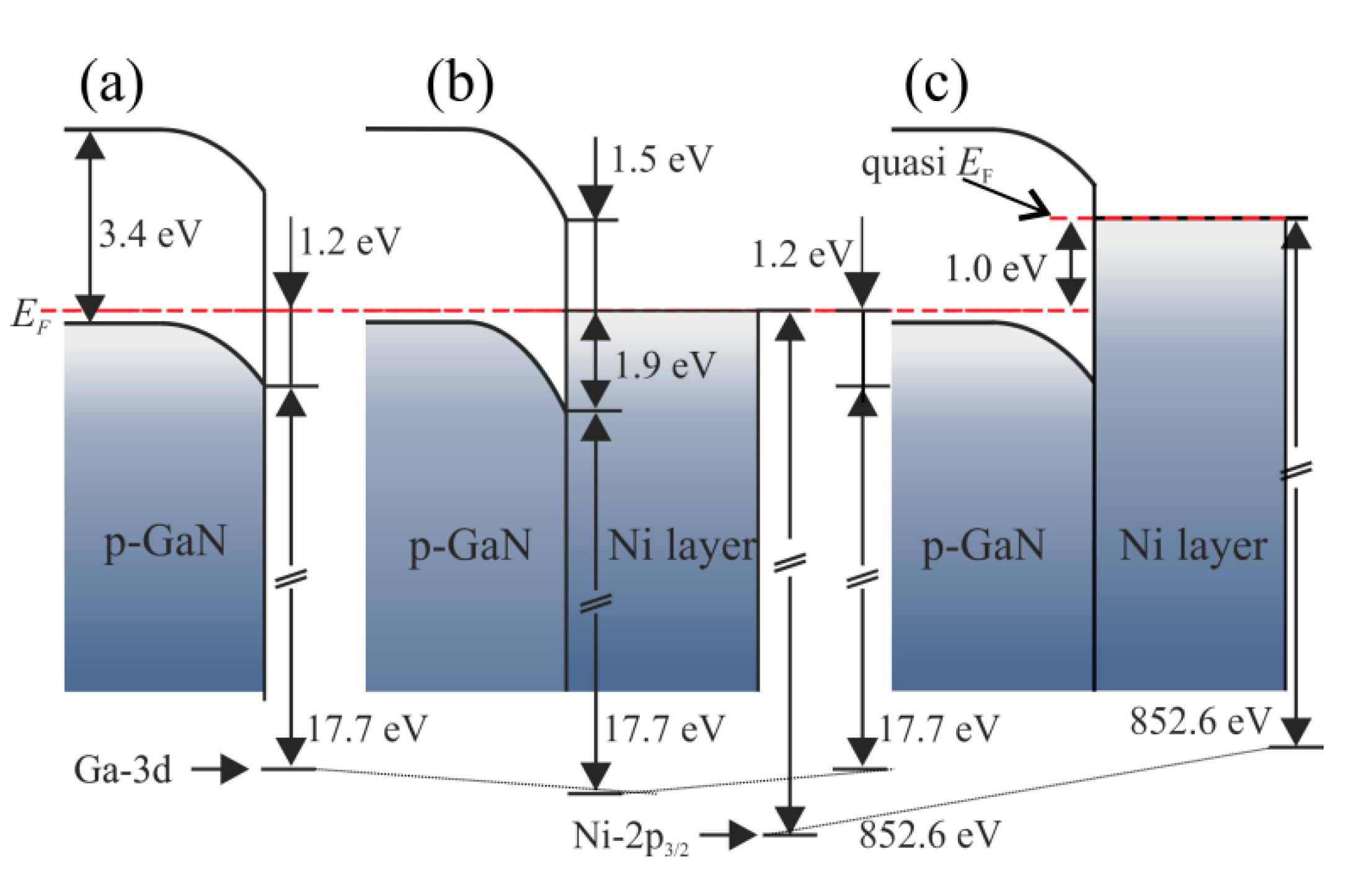
When semiconductors are exposed to photons with a higher energy level than their forbidden gaps, electron–hole pairs are formed. The generation of an electron-hole can also take place in metal/semiconductor systems, especially in the case of thin coating systems [104] and, as a consequence, may result in an appearance of a quasi-Fermi level. Such an effect in the case of Ni film on p-type GaN(0001) was described in [30] and is presented below. Evolutions of the Ga-3d and Ni-2p3/2 core level lines after Ni deposition on a p-type GaN(0001) surface, followed by annealing, are shown in Figure 24. The Ga-3d peak is located at a BE of 18.9 eV for the bare p-GaN(0001) surface and shifts towards a higher BE, to the position of 19.6 eV, after Ni film deposition. According to Mn/GaN (Section 3.2), as well as the Ni/n-GaN systems described above, it is obvious that the shift is related to the Schottky barrier formation. The SBH of Ni on p-GaN for electrons is , and the position of = 1.9 eV (based on the Ga-3d shift), which gives SBH = 1.5 eV. The value of 1.9 eV is the magnitude of SBH for holes.
However, after annealing of the system at 800 °C, the Ga-3d peak moves to its initial position, as shown in Figure 24a, which is unusual. Meanwhile, the Ni-2p3/2 core level line has a BE of 852.6 eV for the as-deposed film and shifts by 1.0 eV towards a lower BE following annealing, as shown in Figure 24b.
It would seem that such a large shift of the Ni line after annealing occurred as a result of a chemical reaction; however, as UPS measurements show, this interpretation is completely wrong. Spectra of the valence band for the bare and Ni film-covered p-GaN(0001), before and after annealing at 800 °C, are shown in Figure 25. The VBM of the p-GaN sample is 1.2 eV below the EF, which gives ∆E = Ga-3d − VBM = 17.7 eV. After the deposition of the thin Ni film of a mean thickness of 1 nm, a DOS nearby the EF increases—the Fermi edge of the Ni film is clearly visible. The VB of the p-GaN is also noticeable in the spectrum, although shifted—its VBM now lies at 1.9 eV. This shift, similar to Ga-3d, is related to the electron charge transfer at the interface, causing the Schottky barrier with an SBH for hole carriers amounting to the above value of 1.9 eV. After annealing, the VBM returns to the starting position, similar to Ga-3G peak behavior. The DOS of the Ni film is still visible but is above the Fermi level of an energy analyzer—a quasi-Fermi level appears at a BE of −1.0 eV. The separation of the Fermi level in the substrate and the thin Ni film causes the shifts of the Ga-3d and Ni-2p3/2 core level lines. The situation is well illustrated in Figure 26.
The presence of the quasi-Fermi level is due to the fact that the uncovering of the GaN surface after annealing exposes the phase boundary for illumination by photons, whose energy is much higher than the forbidden gap of the GaN, resulting in electron-hole pairs being generated there. The p-GaN(0001) surface is more negatively charged compared to the system not annealed (Figure 26b), due to the holes’ transport from the nearby site of the interface to the grounded part of the sample. The Ni-film-covered substrate, after annealing, is in the same condition as the bare surface (Figure 26a,c). Electrons from the valence band near the phase boundary are ejected into the conduction band of the substrate, which is bent downwards, so there is no barrier for them from the metal film side and they may flow down to the Ni film. Thus, this part of the system is more negatively charged. The above section regarding Ni on p-GaN is a good example, showing that some shifts in core level lines observed after annealing do not necessarily have to be the result of an interfacial chemical reaction and may be a consequence of other effects.
Investigations of thin Pd films on GaN(0001) using XPS, UPS, and LEED techniques are summarized in the author’s two publications [34,101]. Such systems have been previously studied with STM [97]. In both works, Pd films were deposited by the PVD method. GaN(0001) n-doped material was used as the substrate. Before depositing the films, LEED images indicated strong spots corresponding to a (1 × 1) structure, with no trace of faceting. No LEED diffraction images for films grown at RT were observed.
In [101], diffraction patterns for Pd films deposited on GaN at room temperature were not observed. The results of the spectroscopic investigation testified that there is no interfacial reaction for the Pd/GaN system created at room temperature. After the deposition of Pd films on the bare n-GaN surface, the Ga-3d core level line shifts from 20.55 to 19.6 eV as a result of the charge transfer at the phase boundary. The valence band maximum, set at 2.75 eV below the Fermi level, was covered by the density of states from the metal, for which the Fermi edge coincided with the EF level of the analyzer. The Pa 3d3/2 line position was located at 335.1 eV binding energy and corresponded to the metallic phase. For the system, similar to the case of the other adsorbates, the Schottky barrier height was estimated. The SBH for the so-prepared system equaled 1.6 eV and was in line with the literature data [28].
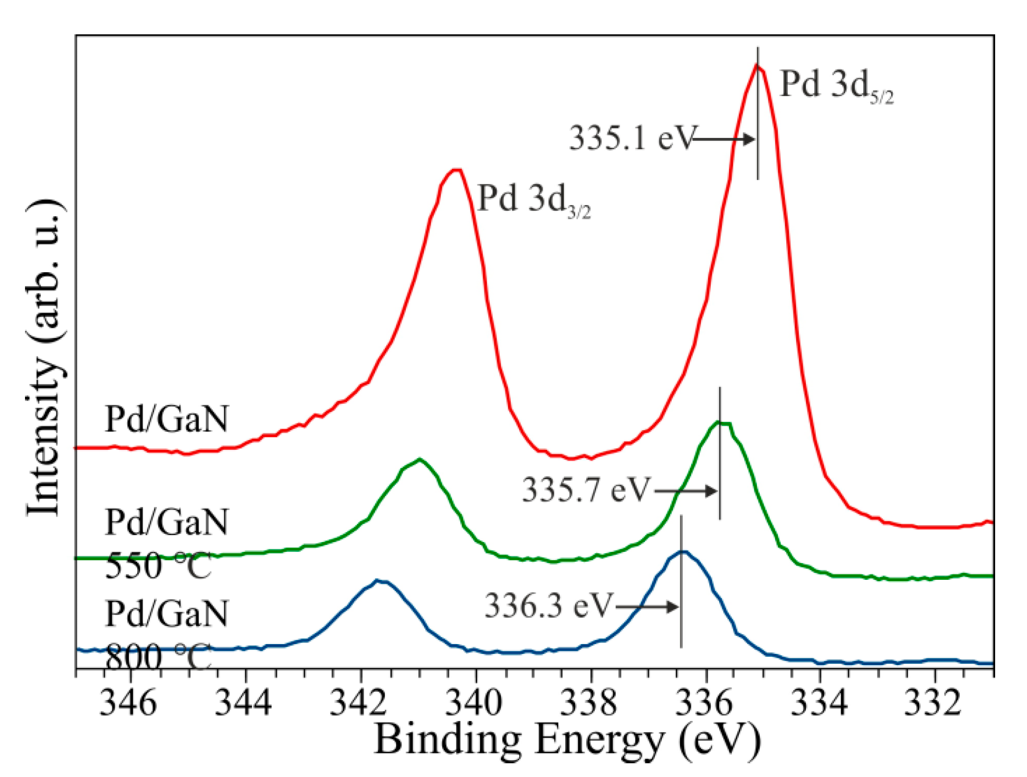
The influence of temperature on the Pd/GaN system has been determined in [34]. The motivation for this research was a potential creation of Pd–Ga alloys on GaN surfaces as a result of the diffusion of Ga atoms from a GaN substrate into thin Pd films. The Pd–Ga alloys (or, actually, intermetallic compounds), such as PdGa, Pd2Ga, and Pd7Ga3, are highly active and stable catalysts in acetylene hydrogenation. This reaction is used in the process of making polyethylene [41].
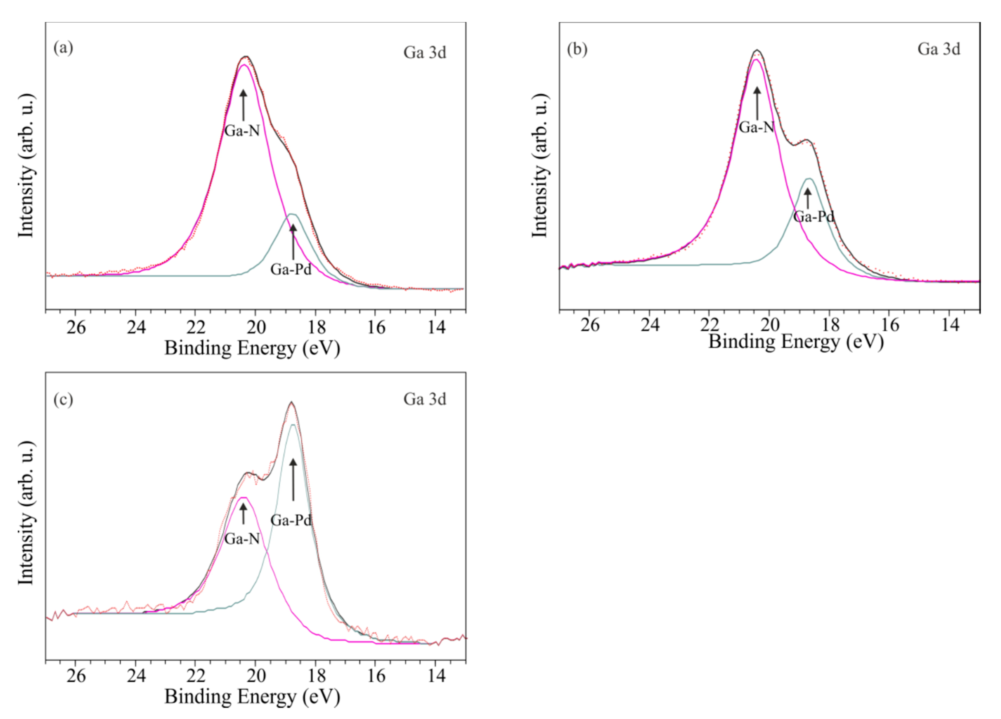
Annealing the Pd/GaN system changes the positions of XPS peaks deriving from the thin film. The Pd-3d line shifts towards higher binding energy. After heating the system at 550 ℃, the Pd-3d5/2 peak takes position at 335.7 eV. This position is typical for the Ga–Pd bonds in the GaPd2 compound [38,39,40]. When further heating the system to 800 ℃, the Pd-3d line will keep moving towards higher binding energies. The Pd-3d5/2 peak is located at 336.3 eV binding energy, which corresponds to the Pd–Ga bond in the GaPd compound. The changes are shown in Figure 27. Heating at 550 ℃ causes an increase in the intensity of Ga-3d and its shift to 20.2 eV.
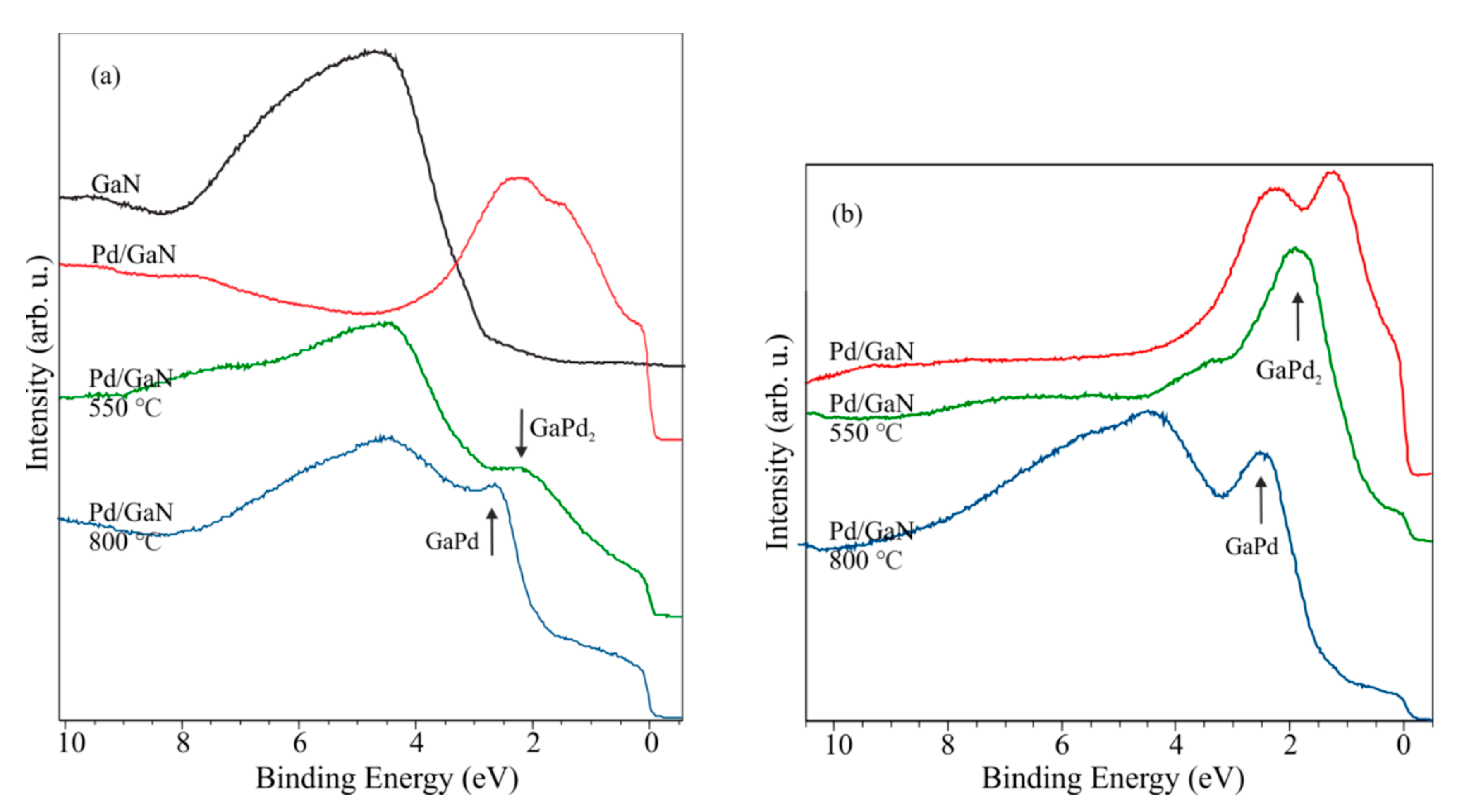
After heating to a higher temperature, the line shifts to the 19.8 eV position, and its intensity continues to increase. This testifies that the surface of the GaN substrate is exposed. This observation is consistent with LEED and STM measurements. After annealing the system at 550 ℃, a blurry LEED image, corresponding to the GaN(0001)-(1 × 1) structure, starts being visible. Annealing at higher temperatures enhances the intensity of the spots and sharpens the image. STM analyses of the system after annealing at lower temperatures indicated an island topography. Islands, varying in diameter and height, were randomly placed on the surface. Additional heating at 800 ℃ caused the population of the islands to decrease, but their diameters and heights increased. UPS spectra made for a bare substrate covered with a thin Pd film, before and after heating at various temperatures, are shown in Figure 28a. The VBM for a bare surface lies at 2.8 eV above the EF; after the deposition of the Pd film, the spectrum has a metallic character. A large density of electronic states near the Fermi level appears. The shape of the valence band, with two maxima at 1.4 and 2.3 eV, corresponds with the literature data. Annealing the system at 550 ℃ leads to a decrease in the density of states of electrons near the Fermi level. An additional maximum appears in the spectrum at around 2.0 eV energy, which is characteristic of the GaPd2 intermetallic system. The other maximum, at around 4.4 eV energy, comes from GaN. In the case of annealing the system at higher temperatures, the valence band structure also undergoes modification. In the spectrum, besides the characteristic maximum coming from GaN, a peak becomes visible at 2.4 eV below the EF level. The shape of the valence band is very similar to the spectrum for GaPd, measured in [40].
XPS peaks from Pd for subsequent Pd films deposited on a previously annealed Pd/GaN system took the same positions as in Figure 27. The change was observed in the case of UPS spectra. In Figure 28b, we can see that the characteristic maxima deriving from the GaPd2 and GaPd compounds are more intense. For a Pd film deposited on a previously annealed Pd/GaN system, a LEED image with a (0.877 × 0.877) structure was observed; no spots coming from the substrate were recorded. The lattice constant equaled 2.79 Å and corresponded to the Pd(111)-(1 × 1) structure; the main crystallographic directions were overlain with the substrate.
Subsequent deposition and annealing cycles led to the growth of crystallites on the surface and the accumulation of GaxPdy compounds on it. Changes in the ratios of the signals coming from the alloy and GaN substrate were observed. It is well illustrated by the Ga-3d line that clearly splits. The evolution of the peak is presented in Figure 29. The component at the higher binding energy derives from the Ga–N bond, whereas at the lower energy level, it derives from the Ga–Pd bond. The energy of the former component equals 20.4 eV; it is 18.7 eV for the latter one. The ratio of bonds Ga–Pd to Ga–N increases after each cycle of depositing and annealing.
3.4. As and Sb on GaN(0001)
Arsenic and antimony are semimetals belonging to the nitrite family in group V on the periodic table. Both of these chemical elements exhibit poor electrical and thermal conductivity properties. Arsenic in its crystal structure has poor metallic properties; however, in an amorphous form, it exhibits semiconductor properties and has a forbidden gap of 1.2 eV [67]. As has a density of 5.75 g/cm3, its thermal conductivity is 50 W/(m·K), and its electrical resistivity amounts to 3 × 10⁻⁷ Ω·m (at RT). It does not melt and starts to sublimate at 615 °C (under standard pressure). It easily evaporates in a vacuum, starting at 107 °C with a vapor pressure of 10−8 mbar, but in the form of various clusters. To eliminate this effect, a special evaporation source with a cracker is needed. Antimony has a density of 6.69 g/cm3, its thermal conductivity is 24 W/(m·K), and its electrical resistivity amounts to 4 × 10⁻⁷ Ω·m (at RT). It melts at 630 °C, and its boiling point is 1635 °C (both values refer to standard pressure). Like arsenic, antimony easily evaporates in a vacuum, starting at 279 °C, with a vapor pressure of 10−8 mbar, and also in the form of various clusters. Both of these elements are used in the electronic industry as a part of semiconductor compounds (e.g., GaAs, InSb) or as n-type dopants for the semiconductor IV-group. Furthermore, there were attempts to use them as surfactants to improve the quality of GaN layers grown by MBE [42,43,44,45,46,47], as well as to form new electronic materials such as GaN(As) and GaN(Sb) alloys. The introduction of As or Sb into GaN causes a modification of the electronic structure of the host material. Both elements cause narrowing of the forbidden gap; in addition, arsenic shifts the VB upwards [48,49,50,51,52,53,54].
A surface study on the interaction of As with GaN(0001) using XPS with a monochromatic Al line and reflection of high-energy electron diffraction (RHEED) was described in the author’s work [57]. The reason for this research is the potential use of arsenic as a means to modify the electronic properties of surfaces. The growth of As film by PVD with a cracker source and its characterization were performed in situ on nondoped MOCVD GaN(0001). The initial bare surface, prepared by RTA at 750 °C, reveals a very small amount of carbon (at the limit of XPS detection) and no oxide contaminant. RHEED exhibits sharp and bright diffraction patterns corresponding to the (1 × 1) structure (not shown). During the growth, the signal of the RHEED patterns decreases with an overlayer thickness of As films. For coatings equal to 2 nm and higher, the patterns disappear completely, suggesting that the film is amorphous. The Ga-3d and As-2p3/2 core level lines and the valence band, prior to and after the deposition of the ~5 nm thick As film, are presented in Figure 22.
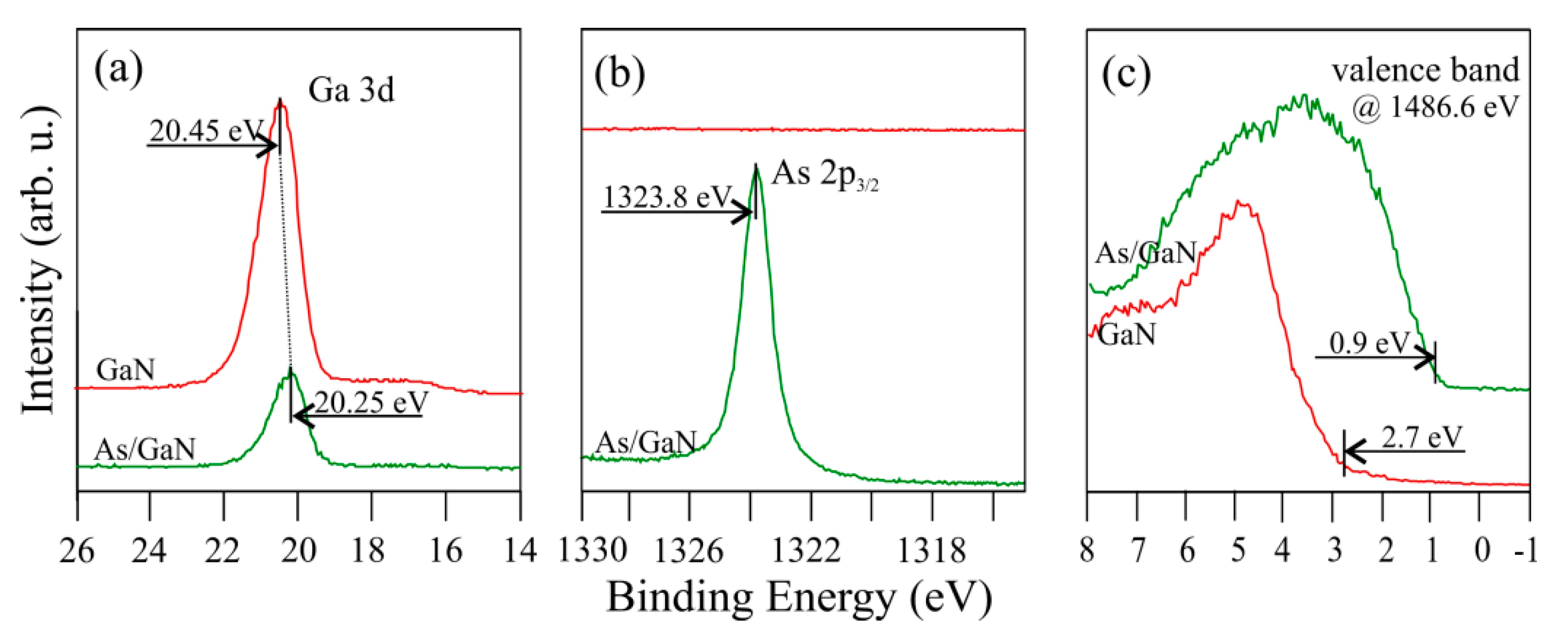
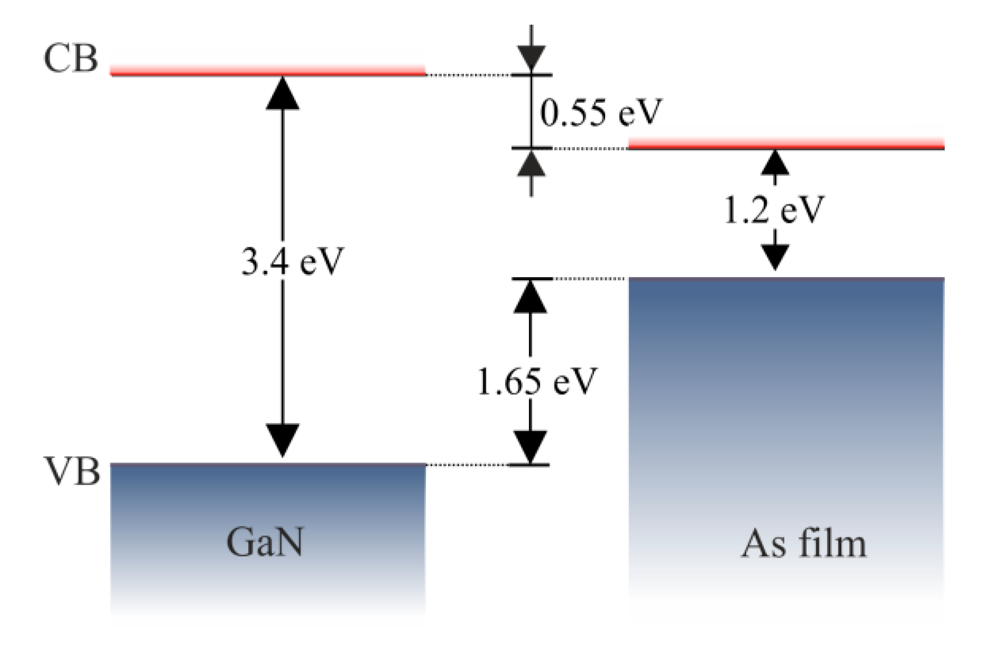
After arsenic deposition on the bare GaN(0001) surface, the Ga-3d core level line shifts towards a lower BE by 0.2 eV to a position of 20.25 eV. As-2p3/2 emerges at a BE of 1323.3 eV and corresponds to As–As bonds [105]. The valence band of the bare GaN(0001) surface is characteristic of typical nondoped GaN. The VBM lies 2.7 eV below the EF, and the energetic distance from it to the Ga-3d state is ∆E = Ga-3d − VBM = 17.7 eV. The DOS of the As film does not start at the Fermi level, as shown in Figure 30c. The edge is shifted towards a higher BE, meaning that the amorphous layers have a semiconductor character for which the VBM is 0.9 eV below the EF. The shift of the Ga-3d peak, shown in Figure 30a, is caused by electrons transfer at the interface, similar to the metal/GaN systems described in Section 3.1 and Section 3.2. However, in this case, instead of SBH, the valence band offset (∆EV) at the phase boundary can be estimated. It can be done based on a method described in [106]. The formula is ∆EV = EV-As2p(As) − EV-Ga3d(GaN) − ∆EAs2p,Ga3d, where EV-As3d(As) and EV-Ga3d(GaN) are the Ga-3d and As-2p3/2d positions relative to the VBM of GaN and As film. Those values are 17.7 and 1322.9 eV, and ∆EAs3d,Ga3d is the energy difference between the As-2p3/2 and Ga-3d levels; when both peaks are visible after the As/GaN interface creation, it amounts to 1303.55 eV. The ∆EV for the As/GaN interface is 1.65 eV. This means that the valence band of As is above the VB of GaN at that value. The conduction band offset (∆EC) can also be evaluated with the formula ∆EC = Eg(As) + ∆EV − Eg(GaN), where values of 1.2 and 3.4 eV are used for the forbidden gap of As film [67] and GaN, respectively. ∆Ec = −0.55 eV; the ‘−’ sign indicates that the conduction band of As is below that of GaN. These values allow us to construct an energy sketch for the As/GaN phase boundary, as shown in Figure 31.
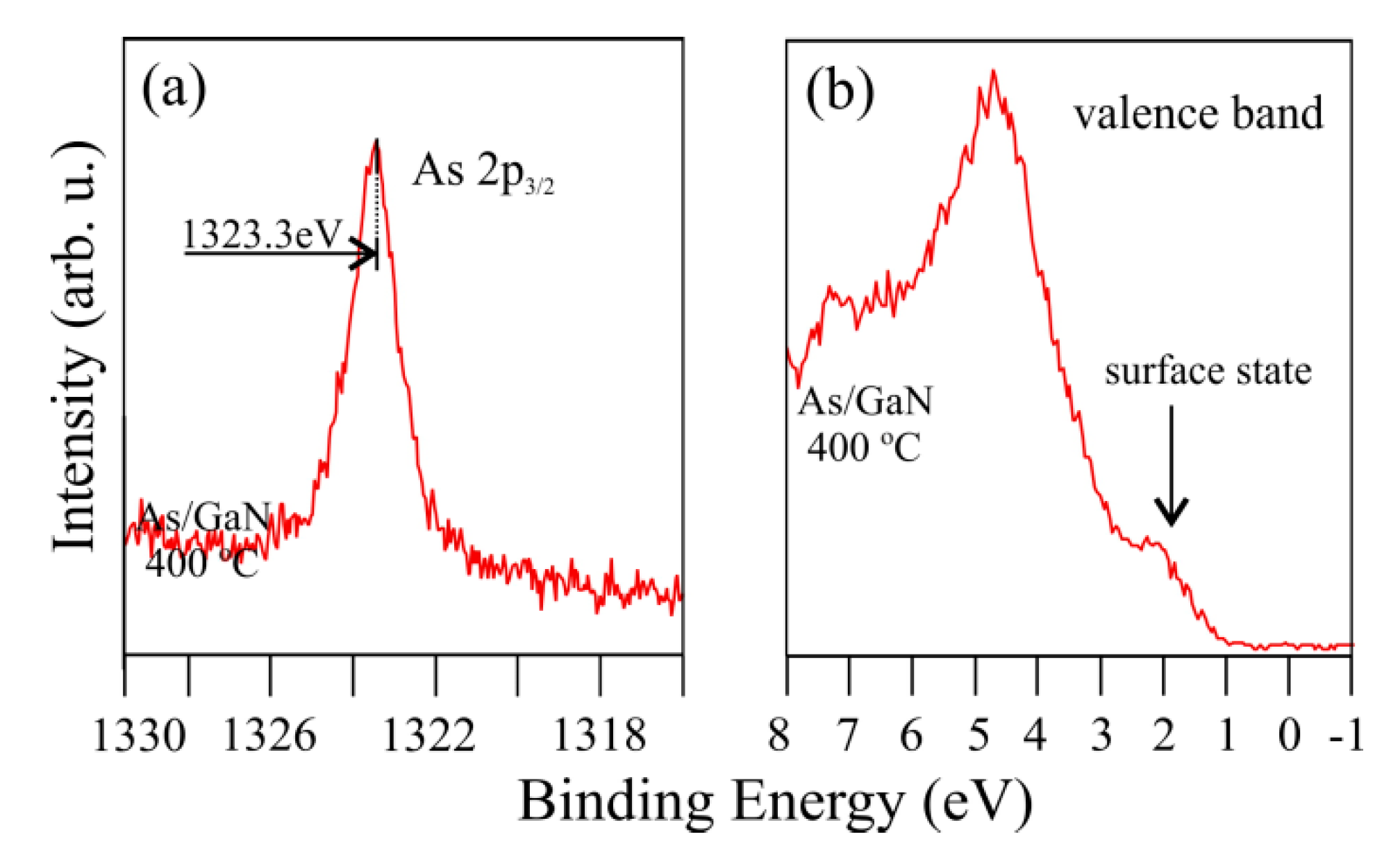
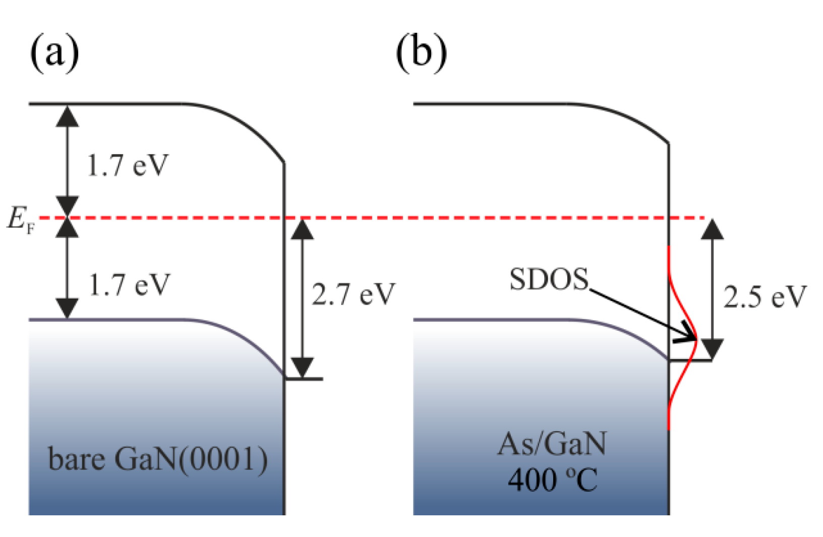
The relatively low As sublimation temperature under UHV conditions should allow As to easily escape from the surface of GaN(0001). Examination of the effect of temperature on the As/GaN system shows that annealing at temperatures below and equal to 200 °C does not introduce significant changes. The As-2p peak intensity decreases slightly after annealing at 200 °C. This is surprising because at 200 °C, arsenic has a relatively high vapor pressure of 10−4 mbar. After annealing at 300 °C, As does not desorb completely from the surface. The As-2p3/2 core level line shifts slightly from 1323.8 to 1323.65 eV, and for temperatures in the range of 350 to 500 °C, the peak shifts further, reaching the position of 1323.3 eV, as shown in Figure 32. This indicates that there has been a chemical interaction of arsenic with the GaN(0001) surface. However, the As-2p3/2 core level line lies at a higher BE than the As–Ga bonding. Therefore, it is possible that arsenic may interact with the surface in the form of As2, as considered in [44]. Repeating the series (As deposition + annealing) does not create new surface alloys on GaN(0001), as in the case of the previously described Ni/GaN system (Section 3.2) or the Pd/GaN system [34]. The condition of the interface remains unchanged, i.e., the XPS lines from the substrate and the adsorbate do not change. In addition, the amount of the fraction As2-GaN(0001) remains unchanged. This is due to the vapor pressure of the adsorbate being much higher than that of gallium (metallic gallium has a vapor pressure of 10−4 mbar at 900 °C). Hence, arsenic atoms escape into the vacuum and have no chance to react with the segregated gallium on the surface. An example of the changes introduced in the valence band by annealing at 400 °C is shown in Figure 32b. The As film thickness for this stage is 0.25 nm. Taking the As density as 1 Å = 4.62 × 10¹⁴ As∙cm−2, one monolayer (ML) on the GaN(0001) surface corresponds to a density of 1.14 × 10¹⁵ atoms∙cm−2. This gives a coverage of As equal to 1 ML. This coverage also explains the lack of growth of the residual arsenic after subsequent cycles of deposition + annealing, as there is no site where it can chemically interact with the GaN(0001) surface.
The surface DOS emerges at a position of 2.2 eV below the Fermi level. Its highest occupied state was found to be at 1.05 eV. Furthermore, the VBM for the system shifts upwards by 0.2 eV, compared to the bare surface, and lies 2.5 below the EF. For this stage of the experiment, RHEED patterns exhibit the clear (1 × 1) structure and Ga-3d is shifted to 20.3 eV. The energy diagrams constructed for the initial bare and As-modified GaN(0001) surfaces are presented in Figure 33.
The SDOS is very visible, even for the system annealed at 500 °C. Further annealing in a temperature range of 600–700 °C of the already annealed system reduces the amount of arsenic. However, this does not completely remove arsenic from the surface. At 700 °C, the As-2p3/2 line shifts to a BE of 1322.85 eV, which corresponds to As–Ga bonds in GaAs crystals [105,107], revealing that arsenic atoms are no longer present at the surface as As2. The residues of the SDOS can still be slightly distinguished in the valence band spectrum. Therefore, it proves that the SDOS is associated with As present on the GaN surface.
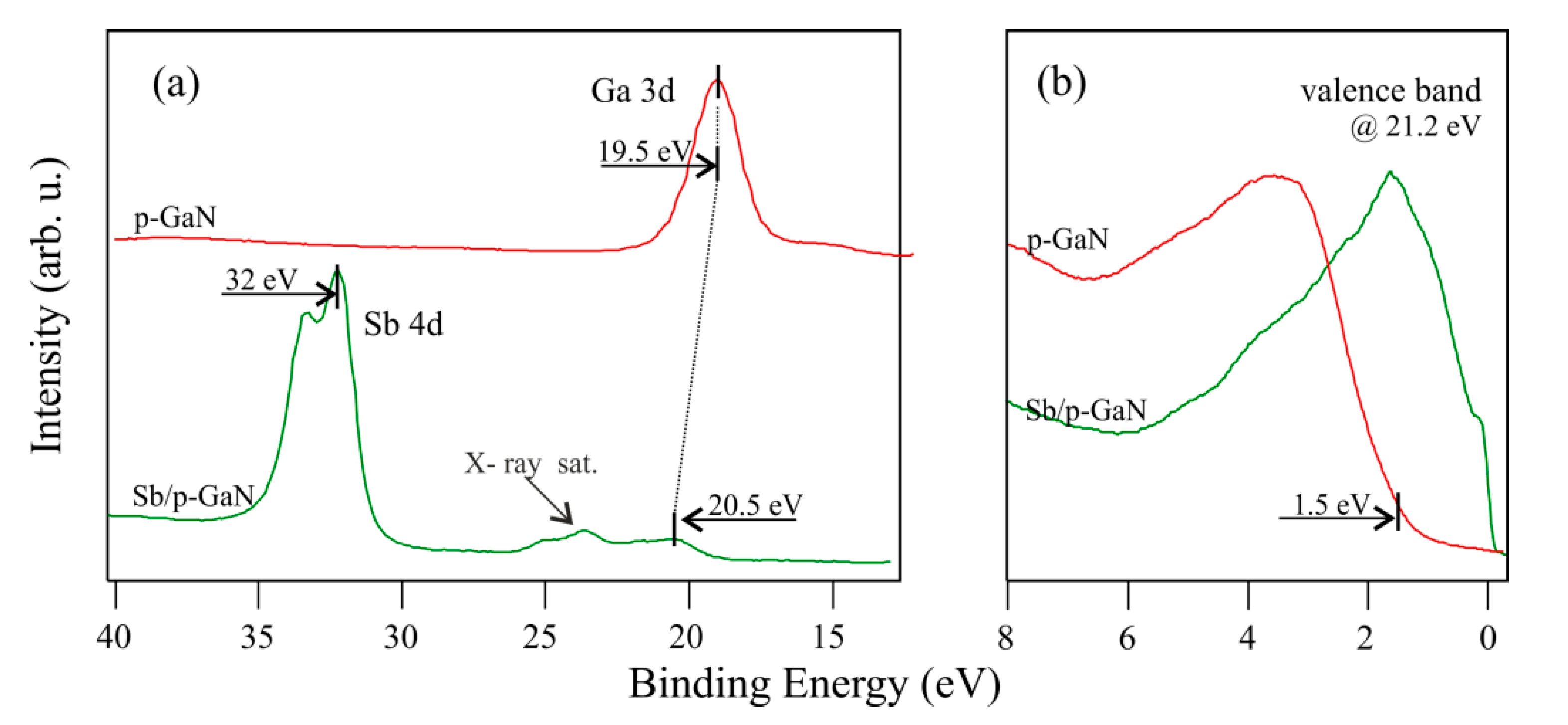
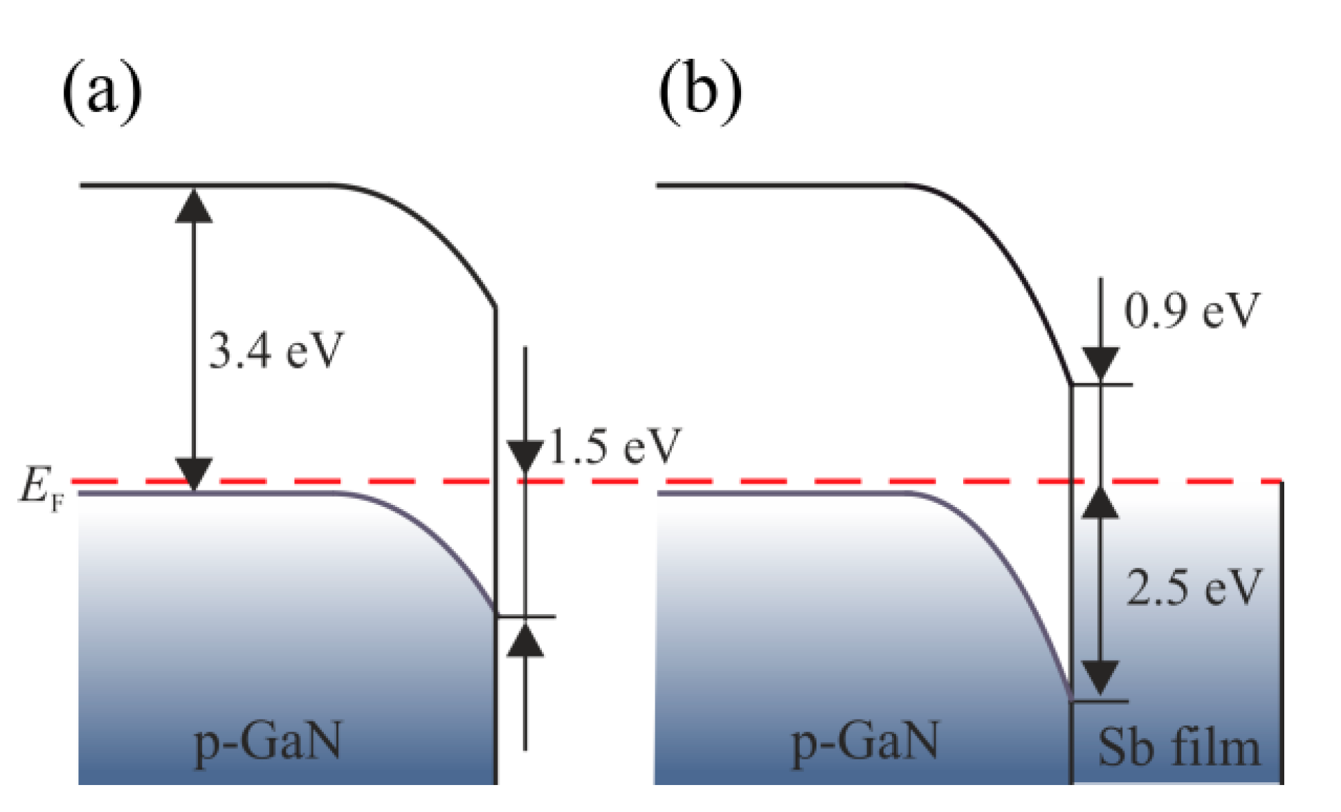
The interaction of the Sb adsorber with the GaN(0001) surface and the morphological changes caused by postdeposition annealing were studied in [58]. The growth of As film by PVD and the surface investigation were carried out in situ on the Mg-doped, p-type, MOCVD GaN(0001) surface. The initial surface was prepared by annealing under UHV conditions. After that, the clean surface revealed a very small amount of oxygen and no carbon (C KLL). LEED exhibited sharp and bright diffraction patterns corresponding to the (1 × 1) structure (similar to that in Figure 5a). LEED did not show diffraction patterns for Sb films deposited at RT on the p-type GaN(0001) surface. This indicates that the Sb layers are amorphous. For the bare surface, the Ga-3d peak is located at 19.5 eV and after deposition of the Sb film, 5 nm thick, the line shifts towards a higher BE to the position 20.5 eV, as shown in Figure 34a. The Sb-4d core level line is located at a BE of 32 eV. The shift of Ga-3d results from the Schottky barrier formation. The VBs of the bare and Sb film-covered GaN(0001) surfaces are presented in Figure 34b. The VBM is located 1.5 eV below the EF for the bare GaN(0001), so it is above the Ga-3d peak by ∆E = Ga-3d − VBM = 17.6 eV. After Sb deposition, the Fermi edge is clearly visible, with a characteristic maximum at 1.6 eV, and the spectrum is similar to that observed for the Sb/SiC system in [108].
The SBH can be calculated using the same procedure in the case of Mn or Ni films on GaN (see Section 3.2 and Section 3.3). The SBH for electrons is , and the position of = 2.5 eV, giving SBH = 0.9 eV, while for the value of 2.5 eV, it is the SBH for holes. The band diagrams for bare and Sb-film-covered GaN(0001) are illustrated in Figure 35.
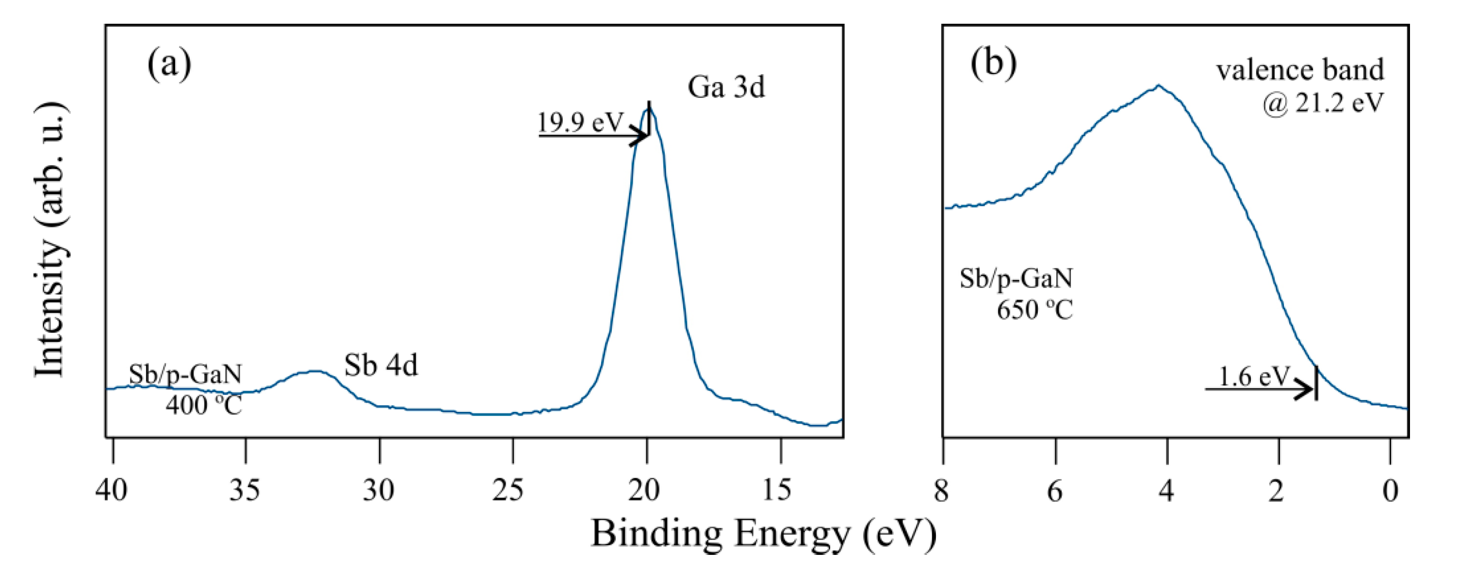
Sb atoms easily desorb from surfaces under UHV conditions, starting at about 280 °C [108]. Therefore, annealing of the Sb/GaN system at 400 °C should lead to a complete desorption of Sb atoms from the GaN(0001) surface. However, the investigation shows the presence of the Sb-3d peak in the XPS spectrum. The position of Sb-4d remains unchanged relative to metallic Sb, which may suggest no chemical interaction with the surface; however, the BE of 32 eV is characteristic of Ga–Sb binding [109]. Considering the annealing temperature and the position of Sb-4d, this indicates that the residual Sb on the surface is in a chemical compound of Ga. Hence, the system under the influence of annealing behaves similarly to As/GaN. The Ga-3d state shifts from 20.5 eV, towards a lower BE, to 19.9 eV, as shown in Figure 36a. The thickness of the residual Sb film is 0.25 nm. Taking the Sb density, 1 Å = 3.31 × 10¹⁴ Sb∙cm−2, this gives a coverage of Sb equal to ~0.7 ML. The UPS spectrum shows a restoration of the valence band of a semiconductor type, with no sign of DOS, unlike in the case of the As/GaN system. The VBM lies at 1.6 eV below the EF, as shown in Figure 36b. In addition to changes in the VBM, the small amount of Sb strongly modifies the vacuum level, which is lower by 1.2 eV compared to the bare surface [57].
4. Summary
Photoelectron spectroscopies (XPS, UPS) were used to investigate properties of bare and film-covered GaN(0001) surfaces.
The bare GaN(0001) was characterized with different X-ray excitation sources, i.e., nonmonochromatic Mg Kα (1253.6 eV) and non- and monochromatic Al Kα (1486.6 eV). Their influence on the shapes of the core level lines and the valence band were found. The type of X-ray source has a particularly large impact on the shape of the N-1s line due to the overlap of the Auger lines that occur for photons with an energy of 1487.6 eV. Significant changes were also observed in the valence band, caused by overlapping with X-ray satellites in the case of nonmonochromatic sources. The binding energy positions of Auger lines vs. X-ray sources are shown. Electronic properties of non- and various doped GaN(0001) surfaces studied by UPS are presented. The valence band maxima lie 2.7 eV below the Fermi level for nondoped GaN and, in the case of doped materials, they are at 3.1 and 1.5 eV for the n- and p-type semiconductors, respectively.
Physical and chemical properties of thin films on GaN(0001), including several elements—manganese, nickel, arsenic, and antimony—were described. Photoelectron spectroscopies were also employed to determine the Schottky barrier height at the formed interfaces. The systems were created in situ on the substrates cleaned by annealing under UHV conditions, and adsorbates were evaporated from Knudsen-like cells. No evidence of epitaxial growth of the films at RT was found.
The investigation of manganese films on GaN(0001) shows that the Schottky barrier height of the interface amounts to 1.20 eV. A chemical interaction of Mn atoms with the substrate at RT was excluded. Annealing the system resulted in morphological changes. Mn atoms and Ga intermixed at the interface. Two effects were found: (i) segregated Ga atoms diffuse into Mn, forming a MnGa surface alloy; (ii) Mn atoms move in the opposite direction, toward the inside of the substrate, and consequently form a (Mn, Ga)N-like alloy. The MnGa surface alloy stays on GaN(0001) after annealing up to 800 °C, achieving a domain structure that is epitaxially oriented, relative to the GaN(0001) substrate. Annealing at a higher temperature can result in removing the MnGa adlayer, but the effect of replacing gallium with manganese atoms in the sublayers of GaN is still visible. It leads to a strong modification of the valence band. The valence band maximum of p-GaN after thermal desorption of the MnGa surface alloy is strongly shifted upwards from 1.5 to 0.1 eV. This result is promising as a stage of preparation of the substrate for Ohmic contacts with p-GaN.
The studies on nickel films on GaN(0001) surfaces show that the Schottky barrier height of the interface with an n-type semiconductor amounts to 1.20 eV, and, with p-types, it is 1.5 and 1.9 eV for electrons and holes, respectively. Annealing the Ni/GaN interface causes the uncovering of the substrate surface. A coalescence of grainy Ni films occurs. Moreover, Ni–Ga surface alloying is exhibited. Ga diffuses into a Ni film and intermixes with it. Ni3Ga is found to be the dominant alloying phase. Further annealing at a higher temperature leads to the formation of a more Ga-rich alloy phase. It is recognized as NiGa or Ni3Ga2.
The Ni/p–GaN interface investigation revealed that the XPS and UPS measurements themselves may affect the electronic structure of the system. Surface conditions of the system were found in which electrons ejected by X-rays or UV penetrated into the metal part of the interface, leading to the film being charged, the consequence of which is the appearance of a quasi-Fermi level, shifting the film’s core level lines. This result is a good example of the fact that some shifts of XPS peaks observed after annealing metal/semiconductor systems may be a consequence of effects other than chemical interactions. Therefore, to explain the reason for this shift, core level measurements are insufficient, and electrons from a valence band should also be monitored.
In the case of thin palladium films on GaN(0001) deposited at RT, no chemical interaction was observed at the phase boundary. The results showed that the Schottky barrier height equaled 1.6 eV. Heating the system caused the uncovering of the substrate surface and the formation of Pd–Ga alloys. In the case of heating to 550 °C, GaPd2 compounds were identified, with chemical bonds deriving from the GaPd compound at higher temperatures. Typical characteristics deriving from GaPd2 and GaPd compounds were observed in the valence band.
The study of arsenic films on GaN(0001) shows that the amorphous films exhibit a semiconductor character. The valence band offset is determined to be 1.65 eV, and the conduction band offset is −0.55 eV, relative to the conduction band of the substrate. A chemical interaction of As atoms with the substrate at RT has been excluded. Annealing the system results in arsenic desorption, although not completely. The residual As atoms chemically interact with the GaN(0001) surface, probably in the form of As2-Ga. Further annealing at a higher temperature means that the As remainders are supposed to chemically react with the surface in the form of As-Ga. The presence of As adatoms at the GaN(0001) surface causes a modification of the valence band — SDOS appears.
The investigation of antimony films on p-GaN(0001) shows that the Schottky barrier height of the interface is 0.9 and 2.50 eV for electrons and holes, respectively. The annealing of the system causes antimony desorption; however, as in the As/GaN system, the Sb atoms are not completely removed. Despite the lack of shift of Sb-4d, it is assumed that residual Sb atoms might have reacted with the substrate since the temperature is too high for metallic Sb atoms to survive on the surface.
Funding
This research was funded by FNP grant number Team Tech/2016-3/16. The APC was funded by Semiconductor Compounds Epitaxy Team, Łukasiewicz Research Network–PORT Polish Center for Technology Development.
Institutional Review Board Statement
Not applicable.
Informed Consent Statement
Not applicable.
Data Availability Statement
The data presented in this study are available on request from the corresponding author.
Acknowledgments
Many thanks to my wife, Anna, and my daughter, Antonine, for their patient and understanding with me while prepering this manuscript. Most results presented in Section 3.1 of this article were obtained at PORT. Other results shown were made during works supported by the University of Wrocław.
Conflicts of Interest
The authors declare no conflict of interest.
References
- Doverspike, K.; Pankove, J. Chapter 9 Doping in the III-Nitrides. In Future Directions in Silicon Photonics; Elsevier BV: Amsterdam, The Netherlands, 1997; Volume 50, pp. 259–277. [Google Scholar]
- Nakamura, S.; Senoh, M.; Mukai, T. Highly P-Typed Mg-Doped GaN Films Grown with GaN Buffer Layers. Jpn. J. Appl. Phys. 1991, 30, L1708–L1711. [Google Scholar] [CrossRef]
- Nakamura, S.; Mukai, T.; Senoh, M.; Iwasa, N. Thermal Annealing Effects on P-Type Mg-Doped GaN Films. Jpn. J. Appl. Phys. 1992, 31, L139–L142. [Google Scholar] [CrossRef]
- Khan, M.A.; Chen, Q.; Shur, M.S.; Dermott, B.; Higgins, J.; Burm, J.; Schaff, W.; Eastman, L. GaN based heterostructure for high power devices. Solid-State Electron. 1997, 41, 1555–1559. [Google Scholar] [CrossRef]
- Yao, T.; Hong, S.-K. (Eds.) Oxide and Nitride Semiconductors: Processing, Properties, and Applications; Springer: Berlin/Heidelberg, Germany, 2009; Available online: www.springer.com/us/book/9783540888468 (accessed on 24 January 2019).
- Flack, T.J.; Pushpakaran, B.; Bayne, S.B. GaN Technology for Power Electronic Applications: A Review. J. Electron. Mater. 2016, 45, 2673–2682. [Google Scholar] [CrossRef]
- Qian, H.; Lee, K.; Vajargah, S.H.; Novikov, S.; Guiney, I.; Zaidi, Z.; Jiang, S.; Wallis, D.; Foxon, C.; Humphreys, C.; et al. Novel GaN-based vertical heterostructure field effect transistor structures using crystallographic KOH etching and overgrowth. J. Cryst. Growth 2017, 459, 185–188. [Google Scholar] [CrossRef]
- Medjdoub, F.; Iniewski, K. Gallium Nitride (GaN); Informa UK Limited: London, UK, 2017. [Google Scholar]
- Mochizuki, K. Vertical GaN and SiC Power Devices; Artech House: Norwood, MA, USA, 2018. [Google Scholar]
- Coffie, R.L. High Power High Frequency Transistors: A Material’s Perspective. In High-Frequency GaN Electronic Devices; Springer Science and Business Media LLC: Berlin/Heidelberg, Germany, 2019; pp. 5–41. [Google Scholar]
- Janicki, L.; Kunert, G.; Sawicki, M.; Piskorska-Hommel, E.; Gas, K.; Jakiela, R.; Hommel, D.; Kudrawiec, R. Fermi level and bands offsets determination in insulating (Ga,Mn)N/GaN structures. Sci. Rep. 2017, 7, 41877. [Google Scholar] [CrossRef] [Green Version]
- Gas, K.; Domagala, J.Z.; Jakieła, R.; Kunert, G.; Dluzewski, P.; Piskorska-Hommel, E.; Paszkowicz, W.; Sztenkiel, D.; Winiarski, M.J.; Kowalska, D.; et al. Impact of substrate temperature on magnetic properties of plasma-assisted molecular beam epitaxy grown (Ga,Mn)N. J. Alloy. Compd. 2018, 747, 946–959. [Google Scholar] [CrossRef] [Green Version]
- Pearton, S.J.; Abernathy, C.; Norton, D.; Hebard, A.F.; Park, Y.; Boatner, L.A.; Budai, J.D. Advances in wide bandgap materials for semiconductor spintronics. Mater. Sci. Eng. R Rep. 2003, 40, 137–168. [Google Scholar] [CrossRef] [Green Version]
- Dietl, T.; Ohno, H. Dilute ferromagnetic semiconductors: Physics and spintronic structures. Rev. Mod. Phys. 2014, 86, 187–251. [Google Scholar] [CrossRef] [Green Version]
- Qi, Y.; Sun, G.F.; Weinert, M.; Li, L. Electronic structures of Mn-induced phases on GaN(0001). Phys. Rev. B 2009, 80, 235323. [Google Scholar] [CrossRef]
- Wang, K.; Takeuchi, N.; Chinchore, A.V.; Lin, W.; Liu, Y.; Smith, A.R. Two-dimensional Mn structure on the GaN growth surface and evidence for room-temperature spin ordering. Phys. Rev. B 2011, 83, 165407. [Google Scholar] [CrossRef] [Green Version]
- Cui, Y.; Li, L. A (10 × 10) domain wall structure induced by Mn adsorption on the pseudo-(1 × 1) surface of GaN. Surf. Sci. 2003, 522, L21–L26. [Google Scholar] [CrossRef]
- Dumont, J.; Kowalski, B.; Pietrzyk, M.; Seldrum, T.; Houssiau, L.; Douhard, B.; Grzegory, I.; Porowski, S.; Sporken, R. Atomically flat GaMnN by diffusion of Mn into GaN(). Superlattices Microstruct. 2006, 40, 607–611. [Google Scholar] [CrossRef]
- Chinchore, A.; Wang, K.; Shi, M.; Liu, Y.; Smith, A.R. Spontaneous formation of quantum height manganese gallium islands and atomic chains on N-polar gallium nitride(0001). Appl. Phys. Lett. 2012, 100, 61602. [Google Scholar] [CrossRef] [Green Version]
- Kowalik, I.A.; Kowalski, B.; Orlowski, B.; Lusakowska, E.; Iwanowski, R.; Mickevičius, S.; Johnson, R.; Grzegory, I.; Porowski, S. Photoemission study of Mn/GaN. Surf. Sci. 2004, 566, 457–461. [Google Scholar] [CrossRef]
- Hwang, J.I.; Osafune, Y.; Kobayashi, M.; Ebata, K.; Ooki, Y.; Ishida, Y.; Fujimori, A.; Takeda, Y.; Okane, T.; Saitoh, Y.; et al. Depth profile high-energy spectroscopic study of Mn-doped GaN prepared by thermal diffusion. J. Appl. Phys. 2007, 101, 103709. [Google Scholar] [CrossRef] [Green Version]
- Grodzicki, M.; Mazur, P.; Krupski, A.; Ciszewski, A. Studies of early stages of Mn/GaN(0001) interface formation using surface-sensitive techniques. VAC 2018, 153, 12–16. [Google Scholar] [CrossRef] [Green Version]
- Grodzicki, M.; Mazur, P.; Brona, J.; Ciszewski, A. MnGa and (Mn,Ga)N-like alloy formation during annealing of Mn/GaN(0001) interface. Appl. Surf. Sci. 2019, 481, 790–794. [Google Scholar] [CrossRef]
- Grodzicki, M.; Mazur, P.; Sabik, A. Electronic properties of p-GaN co-doped with Mn by thermal process: Surface studies. Surf. Sci. 2019, 689, 121460. [Google Scholar] [CrossRef]
- Bermudez, V.M.; Kaplan, R.; Khan, M.A.; Kuznia, J.N. Growth of thin Ni films on GaN(0001)-(1 × 1). Phys. Rev. B 1993, 48, 2436–2444. [Google Scholar] [CrossRef]
- Schmitz, A.C.; Ping, A.T.; Khan, M.A.; Chen, Q.; Yang, J.W.; Adesida, I. Schottky barrier properties of various metals on n-type GaN. Semicond. Sci. Technol. 1996, 11, 1464–1467. [Google Scholar] [CrossRef]
- Schmitz, A.; Ping, A.; Adesida, I.; Khan, M.A. Schottky Barrier Heights of Ni, Pt, Pd, and Au on n-type GaN. MRS Proc. 1995, 395, 831–835. [Google Scholar] [CrossRef]
- Rickert, K.A.; Ellis, A.; Kim, J.K.; Lee, J.-L.; Himpsel, F.J.; Dwikusuma, F.; Kuech, T.F. X-ray photoemission determination of the Schottky barrier height of metal contacts to n–GaN and p–GaN. J. Appl. Phys. 2002, 92, 6671–6678. [Google Scholar] [CrossRef] [Green Version]
- Grodzicki, M.; Mazur, P.; Zuber, S.; Perš, J.; Brona, J.; Ciszewski, A. Effect of annealing on Ni/GaN(0001) contact morphology. Appl. Surf. Sci. 2014, 304, 24–28. [Google Scholar] [CrossRef]
- Grodzicki, M.; Mazur, P.; Sabik, A. Impact of surface photovoltage on photoemission from Ni/p-GaN. Appl. Surf. Sci. 2020, 512, 145643. [Google Scholar] [CrossRef]
- Greco, G.; Iucolano, F.; Roccaforte, F. Ohmic contacts to Gallium Nitride materials. Appl. Surf. Sci. 2016, 383, 324–345. [Google Scholar] [CrossRef]
- Wang, W.; Xie, W.; Deng, Z.; Yang, H.; Liao, M.; Li, J.; Luo, X.; Sun, S.; Zhao, D. Performance Improvement of GaN Based Laser Diode Using Pd/Ni/Au Metallization Ohmic Contact. Coatings 2019, 9, 291. [Google Scholar] [CrossRef] [Green Version]
- Li, M.; Li, C.; Wang, F.; Zhang, W. The thermodynamic analysis of the driving force for the Ni/GaN interfacial reaction. Mater. Sci. Eng. A 2006, 422, 316–320. [Google Scholar] [CrossRef]
- Grodzicki, M.; Mazur, P.; Pers, J.; Brona, J.; Zuber, S.; Ciszewski, A. Formation of GaPd2 and GaPd intermetallic compounds on GaN(0001). Appl. Phys. A 2015, 120, 1443–1451. [Google Scholar] [CrossRef]
- Sharafutdinov, I.; Elkjær, C.F.; De Carvalho, H.W.P.; Gardini, D.; Chiarello, G.L.; Damsgaard, C.D.; Wagner, J.B.; Grunwaldt, J.-D.; Dahl, S.; Chorkendorff, I. Intermetallic compounds of Ni and Ga as catalysts for the synthesis of methanol. J. Catal. 2014, 320, 77–88. [Google Scholar] [CrossRef]
- Studt, F.; Sharafutdinov, I.; Abild-Pedersen, F.; Elkjær, C.F.; Hummelshøj, J.S.; Dahl, S.; Chorkendorff, I.; Nørskov, J.K. Discovery of a Ni-Ga catalyst for carbon dioxide reduction to methanol. Nat. Chem. 2014, 6, 320–324. [Google Scholar] [CrossRef] [PubMed]
- Kovnir, K.; Armbrüster, M.; Teschner, D.; Venkov, T.; Jentoft, F.; Knop-Gericke, A.; Grin, Y.; Schlögl, R. A new approach to well-defined, stable and site-isolated catalysts. Sci. Technol. Adv. Mater. 2007, 8, 420–427. [Google Scholar] [CrossRef]
- Osswald, J.; Giedigkeit, R.; Jentoft, R.; Armbrüster, M.; Girgsdies, F.; Kovnir, K.; Ressler, T.; Grin, Y.; Schlögl, R. Palladium–gallium intermetallic compounds for the selective hydrogenation of acetylenePart I: Preparation and structural investigation under reaction conditions. J. Catal. 2008, 258, 210–218. [Google Scholar] [CrossRef]
- Osswald, J.; Kovnir, K.; Armbrüster, M.; Giedigkeit, R.; Jentoft, R.E.; Wild, U.; Grin, Y.; Schlögl, R. Palladium–gallium intermetallic compounds for the selective hydrogenation of acetylenePart II: Surface characterization and catalytic performance. J. Catal. 2008, 258, 219–227. [Google Scholar] [CrossRef]
- Kovnir, K.; Armbrüster, M.; Teschner, D.; Venkov, T.; Szentmiklósi, L.; Jentoft, F.; Knop-Gericke, A.; Grin, Y.; Schlögl, R. In situ surface characterization of the intermetallic compound PdGa–A highly selective hydrogenation catalyst. Surf. Sci. 2009, 603, 1784–1792. [Google Scholar] [CrossRef] [Green Version]
- Armbrüster, M.; Schlögl, R.; Grin, Y. Intermetallic compounds in heterogeneous catalysis—A quickly developing field. Sci. Technol. Adv. Mater. 2014, 15, 34803. [Google Scholar] [CrossRef] [PubMed]
- Foxon, C.; Cheng, T.; Novikov, S.; Jeffs, N.; Hughes, O.; Melnik, Y.; Nikolaev, A.E.; Dmitriev, V. Gallium-induced surface reconstruction patterns of GaN grown by molecular beam epitaxy. Surf. Sci. 1999, 421, 377–385. [Google Scholar] [CrossRef]
- Hughes, O.; Cheng, T.; Novikov, S.; Foxon, C.; Korakakis, D.; Jeffs, N. RHEED studies of the GaN surface during growth by molecular beam epitaxy. J. Cryst. Growth 1999, 201, 388–391. [Google Scholar] [CrossRef]
- Ramachandran, V.; Lee, C.; Feenstra, R.M.; Smith, A.; Northrup, J.; Greve, D. Structure of clean and arsenic-covered GaN(0001) surfaces. J. Cryst. Growth 2000, 209, 355–363. [Google Scholar] [CrossRef]
- Vézian, S.; Semond, F.; Massies, J.; Bullock, D.; Ding, Z.; Thibado, P. Origins of GaN(0001) surface reconstructions. Surf. Sci. 2003, 541, 242–251. [Google Scholar] [CrossRef] [Green Version]
- Pei, C.W.; Turk, B.; Héroux, J.B.; Wang, W.I. GaN grown by molecular beam epitaxy with antimony as surfactant. J. Vac. Sci. Technol. B Microelectron. Nanometer Struct. 2001, 19, 1426. [Google Scholar] [CrossRef]
- Gokhale, A.A.; Kuech, T.F.; Mavrikakis, M. Surfactant effect of Sb on GaN growth. J. Cryst. Growth 2005, 285, 146–155. [Google Scholar] [CrossRef]
- Shan, W.; Ager, J.W.; Yu, K.; Walukiewicz, W.; Haller, E.E.; Martín, M.C.; McKinney, W.R.; Yang, W. Dependence of the fundamental band gap of AlxGa1−xN on alloy composition and pressure. J. Appl. Phys. 1999, 85, 8505–8507. [Google Scholar] [CrossRef]
- Wu, J.; Walukiewicz, W.; Yu, K.M.; Denlinger, J.D.; Shan, W.; Ager, J.W.; Kimura, A.; Tang, H.F.; Kuech, T.F. Valence band hybridization in N-rich GaN(1-x)As(x) alloys. Phys. Rev. B 2004, 70, 115214. [Google Scholar] [CrossRef] [Green Version]
- Zdanowicz, E.; Ciechanowicz, P.; Opołczyńska, K.; Majchrzak, D.; Rousset, J.-G.; Piskorska-Hommel, E.; Grodzicki, M.; Komorowska, K.; Serafinczuk, J.; Hommel, D.; et al. As-related stability of the band gap temperature dependence in N-rich GaNAs. Appl. Phys. Lett. 2019, 115, 092106. [Google Scholar] [CrossRef]
- Grodzicki, M.; Rousset, J.-G.; Ciechanowicz, P.; Piskorska-Hommel, E.; Hommel, D. XPS studies on the role of arsenic incorporated into GaN. VAC 2019, 167, 73–76. [Google Scholar] [CrossRef]
- Yu, K.; Sarney, W.L.; Novikov, S.; Detert, D.; Zhao, R.; Denlinger, J.D.; Svensson, S.; Dubon, O.D.; Walukiewicz, W.; Foxon, C. Highly mismatched N-rich GaN1−xSbx films grown by low temperature molecular beam epitaxy. Appl. Phys. Lett. 2013, 102, 102104. [Google Scholar] [CrossRef]
- Yu, K.; Novikov, S.; Ting, M.; Sarney, W.L.; Svensson, S.; Shaw, M.; Martin, R.W.; Walukiewicz, W.; Foxon, C. Growth and characterization of highly mismatched GaN1−xSbx alloys. J. Appl. Phys. 2014, 116, 123704. [Google Scholar] [CrossRef] [Green Version]
- Segercrantz, N.; Yu, K.; Ting, M.; Sarney, W.L.; Svensson, S.; Novikov, S.; Foxon, C.; Walukiewicz, W. Electronic band structure of highly mismatched GaN1−xSbx alloys in a broad composition range. Appl. Phys. Lett. 2015, 107, 142104. [Google Scholar] [CrossRef] [Green Version]
- Thao, C.P.; Tuan, T.T.A.; Kuo, D.-H.; Ke, W.-C.; Na Thach, T.V.S.; Cao, P.T. Reactively Sputtered Sb-GaN Films and its Hetero-Junction Diode: The Exploration of the n-to-p Transition. Coatings 2020, 10, 210. [Google Scholar] [CrossRef] [Green Version]
- Segercrantz, N.; Baumgartner, Y.; Ting, M.; Yu, K.; Mao, S.S.; Sarney, W.L.; Svensson, S.; Walukiewicz, W. Undoped p-type GaN1–xSbx alloys: Effects of annealing. Appl. Phys. Lett. 2016, 109, 252102. [Google Scholar] [CrossRef] [Green Version]
- Grodzicki, M.; Rousset, J.-G.; Ciechanowicz, P.; Piskorska-Hommel, E.; Hommel, D. Surface studies of physicochemical properties of As films on GaN(0001). Appl. Surf. Sci. 2019, 493, 384–388. [Google Scholar] [CrossRef]
- Grodzicki, M.; Mazur, P.; Pers, J.; Zuber, S.; Ciszewski, A. Sb Layers on p-GaN: UPS, XPS and LEED Study. Acta Phys. Pol. A 2014, 126, 1128–1130. [Google Scholar] [CrossRef]
- Feenstra, R.M.; Northrup, J.E.; Neugebauer, J. Review of Structure of Bare and Adsorbate-Covered GaN(0001) Surfaces. MRS Internet J. Nitride Semicond. Res. 2002, 7. [Google Scholar] [CrossRef] [Green Version]
- Eller, B.S.; Yang, J.; Nemanich, R.J. Electronic surface and dielectric interface states on GaN and AlGaN. J. Vac. Sci. Technol. A 2013, 31, 050807. [Google Scholar] [CrossRef]
- Bermudez, V. The fundamental surface science of wurtzite gallium nitride. Surf. Sci. Rep. 2017, 72, 147–315. [Google Scholar] [CrossRef]
- Majchrzak, D.; Grodzicki, M.; Ciechanowicz, P.; Rousset, J.; Piskorska-Hommel, E.; Hommel, D. The Influence of Oxygen and Carbon Contaminants on the Valence Band of p-GaN(0001). Acta Phys. Pol. A 2019, 136, 585–588. [Google Scholar] [CrossRef]
- Long, J.P.; Bermudez, V.M. Band bending and photoemission-induced surface photovoltages on clean n—And p -GaN(0001) surfaces. Phys. Rev. B 2002, 66, 121308. [Google Scholar] [CrossRef] [Green Version]
- Grodzicki, M.; Moszak, K.; Hommel, D.; Bell, G.R. Band alignment and surface Fermi level pinning in GaN. Appl. Surf. Sci. 2020, 533, 147416. [Google Scholar] [CrossRef]
- Pugh, S.; Dugdale, D.; Brand, S.; Abram, R. Electronic Structure Calculations on Nitride Semiconductors. Semicond. Sci. Technol. 1999, 14, 23. [Google Scholar] [CrossRef]
- Madelung, O. Semiconductors; Springer Science and Business Media LLC: Berlin/Heidelberg, Germany, 1991. [Google Scholar]
- Madelung, O.; Madelung, O. Semiconductors: Data Handbook; Springer: Berlin, Germany, 2004. [Google Scholar]
- Levinshtein, M.E.; Rumyantsev, S.L.; Shur, M.S. Properties of Advanced Semiconductor Materials: GaN, AIN, InN, BN, SiC, SiGe|Wiley, 2001. Available online: https://www.wiley.com/en-us/Properties+of+Advanced+Semiconductor+Materials%3A+GaN%2C+AIN%2C+InN%2C+BN%2C+SiC%2C+SiGe-p-9780471358275 (accessed on 28 April 2020).
- Falta, J.; Schmidt, T.; Gangopadhyay, S.; Schulz, C.; Kuhr, S.; Berner, N.; Flege, J.I.; Pretorius, A.; Rosenauer, A.; Sebald, K.; et al. Cleaning and growth morphology of GaN and InGaN surfaces. Phys. Status Solidi (b) 2011, 248, 1800–1809. [Google Scholar] [CrossRef]
- Kova, J.; Zalar, A.; Kovač, J. Surface composition changes in GaN induced by argon ion bombardment. Surf. Interface Anal. 2002, 34, 253–256. [Google Scholar] [CrossRef]
- Despiau-Pujo, E.; Chabert, P. MD simulations of GaN sputtering by Ar+ ions: Ion-induced damage and near-surface modification under continuous bombardment. J. Vac. Sci. Technol. A 2010, 28, 1105. [Google Scholar] [CrossRef]
- Hunt, R.; Vanzetti, L.; Castro, T.; Chen, K.; Sorba, L.; Cohen, P.; Gladfelter, W.; Van Hove, J.; Kuznia, J.; Khan, M.; et al. Electronic structure, surface composition and long-range order in GaN. Phys. B Condens. Matter 1993, 185, 415–421. [Google Scholar] [CrossRef]
- Grodzicki, M.; Mazur, P.; Ciszewski, A. Modification of Electronic Structure of n-GaN(0001) Surface by N+-Ion Bombardment. Acta Phys. Pol. A 2017, 132, 351–353. [Google Scholar] [CrossRef]
- Grodzicki, M.; Mazur, P.; Ciszewski, A. Changes of electronic properties of p-GaN(0 0 0 1) surface after low-energy N+-ion bombardment. Appl. Surf. Sci. 2018, 440, 547–552. [Google Scholar] [CrossRef]
- Koleske, D.; Wickenden, A.E.; Henry, R.; DeSisto, W.J.; Gorman, R.J. Growth model for GaN with comparison to structural, optical, and electrical properties. J. Appl. Phys. 1998, 84, 1998–2010. [Google Scholar] [CrossRef]
- Janzen, O.; Hahn, C.; Kampen, T.; Mönch, W. Explanation of multiplet spots in low-energy electron diffraction patterns of clean GaN surfaces. Eur. Phys. J. B 1999, 7, 1–4. [Google Scholar] [CrossRef]
- Tautz, F.; Sloboshanin, S.; Starke, U.; Schaefer, J. Reactivity and morphology of (10-1-2)-faceted and (3 × 3)-reconstructed GaN(000-1) epilayers grown on sapphire (0001). J. Phys. Condens. Matter 1999, 11, 8035. [Google Scholar] [CrossRef]
- Segev, D.; Van De Walle, C.G. Origins of Fermi-level pinning on GaN and InN polar and nonpolar surfaces. EPL (Europhysics Lett. 2006, 76, 305–311. [Google Scholar] [CrossRef]
- Van De Walle, C.G.; Segev, D. Microscopic origins of surface states on nitride surfaces. J. Appl. Phys. 2007, 101, 081704. [Google Scholar] [CrossRef] [Green Version]
- Janicki, Ł.; Gładysiewicz, M.; Misiewicz, J.; Klosek, K.; Sobanska, M.; Kempisty, P.; Zytkiewicz, Z.R.; Kudrawiec, R. Contactless electroreflectance studies of the Fermi level position at the air/GaN interface: Bistable nature of the Ga-polar surface. Appl. Surf. Sci. 2017, 396, 1657–1666. [Google Scholar] [CrossRef]
- Shi, M.; Chinchore, A.; Wang, K.; Mandru, A.-O.; Liu, Y.; Smith, A.R. Formation of manganese δ-doped atomic layer in wurtzite GaN. J. Appl. Phys. 2012, 112, 53517. [Google Scholar] [CrossRef]
- Chinchore, A.; Wang, K.; Lin, W.; Pak, J.; Smith, A.R. Atomic layer structure of manganese atoms on wurtzite gallium nitride (000 1). Appl. Phys. Lett. 2008, 93, 181908. [Google Scholar] [CrossRef] [Green Version]
- Chinchore, A.V.; Wang, K.; Shi, M.; Mandru, A.; Liu, Y.; Haider, M.; Smith, A.R.; Ferrari, V.; Barral, M.A.; Ordejon, P. Manganese 3 × 3 and 3 × 3—R30° structures and structural phase transition on w -GaN(000 1¯) studied by scanning tunneling microscopy and first-principles theory. Phys. Rev. B 2013, 87, 165426. [Google Scholar] [CrossRef] [Green Version]
- Waldrop, J.R.; Grant, R.W.; Wang, Y.C.; Davis, R.F. Metal Schottky barrier contacts to alpha 6H-SiC. J. Appl. Phys. 1992, 72, 4757–4760. [Google Scholar] [CrossRef]
- Waldrop, J.R. Schottky barrier height of metal contacts to p-type alpha 6H-SiC. J. Appl. Phys. 1994, 75, 4548–4550. [Google Scholar] [CrossRef]
- Reed, M.; Ritums, M.; Stadelmaier, H.; Reed, M.; Parker, C.; Bedair, S.; El-Masry, N. Room temperature magnetic (Ga,Mn)N: A new material for spin electronic devices. Mater. Lett. 2001, 51, 500–503. [Google Scholar] [CrossRef]
- Reed, M.L.; El-Masry, N.A.; Stadelmaier, H.H.; Ritums, M.K.; Reed, M.J.; Parker, C.A.; Roberts, J.C.; Bedair, S.M. Room temperature ferromagnetic properties of (Ga, Mn)N. Appl. Phys. Lett. 2001, 79, 3473–3475. [Google Scholar] [CrossRef]
- Hobbs, D.; Hafner, J.; Spišák, D. Understanding the complex metallic element Mn. I. Crystalline and noncollinear magnetic structure of α-Mn. Phys. Rev. B 2003, 68. [Google Scholar] [CrossRef] [Green Version]
- Lu, Q.M.; Yue, M.; Zhang, H.G.; Wang, M.L.; Yu, F.; Huang, Q.Z.; Ryan, D.H.; Altounian, Z. Intrinsic magnetic properties of single-phase Mn1+xGa (0 < x < 1) alloys. Sci. Rep. 2015, 5, 17086. [Google Scholar] [CrossRef] [PubMed] [Green Version]
- Arins, A.; Jurca, H.; Zarpellon, J.; Fabrim, Z.; Fichtner, P.F.P.; Varalda, J.; Schreiner, W.; Mosca, D. Correlation between tetragonal zinc-blende structure and magnetocrystalline anisotropy of MnGa epilayers on GaAs(111). J. Magn. Magn. Mater. 2015, 381, 83–88. [Google Scholar] [CrossRef]
- Hwang, J.I.; Ishida, Y.; Kobayashi, M.; Hirata, H.; Takubo, K.; Mizokawa, T.; Fujimori, A.; Okamoto, J.; Mamiya, K.; Saito, Y.; et al. High-energy spectroscopic study of the III-V nitride-based diluted magnetic semiconductorGa1−xMnxN. Phys. Rev. B 2005, 72, 085216. [Google Scholar] [CrossRef] [Green Version]
- Brudnyi, V.N. Gallium Nitride: Charge Neutrality Level and Interfaces. Russ. Phys. J. 2016, 58, 1613–1618. [Google Scholar] [CrossRef]
- Majid, A.; Ahmad, N.; Rizwan, M.; Khan, S.U.-D.; Ali, F.A.A.; Zhu, J. Effects of Mn Ion Implantation on XPS Spectroscopy of GaN Thin Films. J. Electron. Mater. 2017, 47, 1555–1559. [Google Scholar] [CrossRef]
- Kulatov, E.; Nakayama, H.; Mariette, H.; Ohta, H.; Uspenskii, Y.A. Electronic structure, magnetic ordering, and optical properties of GaN and GaAs doped with Mn. Phys. Rev. B 2002, 66, 045203. [Google Scholar] [CrossRef]
- Barthel, S.; Kunert, G.; Gartner, M.; Stoica, M.; Mourad, D.; Kruse, C.; Figge, S.; Hommel, D.; Czycholl, G. Determination of the Fermi level position in dilute magnetic Ga1-xMnxN films. J. Appl. Phys. 2014, 115, 123706. [Google Scholar] [CrossRef] [Green Version]
- Titov, A.; Biquard, X.; Halley, D.; Kuroda, S.; Bellet-Amalric, E.; Mariette, H.; Cibert, J.; Merad, A.E.; Merad, G.; Kanoun, M.-B.; et al. X-ray absorption near-edge structure and valence state of Mn in (Ga,Mn)N. Phys. Rev. B 2005, 72, 115209. [Google Scholar] [CrossRef]
- Nörenberg, C.; Myhra, S.; Dobson, P.J. Scanning probe microscopy studies on the growth of palladium and nickel on GaN(0001). J. Phys. Conf. Ser. 2010, 209, 012021. [Google Scholar] [CrossRef]
- Pers, J.; Grodzicki, M.; Ciszewski, A. Topography of thin films containing Ni-Ga intermetallic compounds formed on GaN(0001). Copernic. Lett. 2016, 7, 1. [Google Scholar] [CrossRef]
- Maruyama, T.; Hagio, Y.; Miyajima, T.; Kijima, S.; Nanishi, Y.; Akimoto, K. Effects of annealing on the interface properties between ni and p-gan. Phys. Status Solidi (A) 2001, 188, 375–378. [Google Scholar] [CrossRef]
- Barinov, A.; Gregoratti, L.; Kaulich, B.; Kiskinova, M.; Rizzi, A. Defect-induced lateral chemical heterogeneity at Ni/GaN interfaces and its effect on the electronic properties of the interface. Appl. Phys. Lett. 2001, 79, 2752–2754. [Google Scholar] [CrossRef]
- Grodzicki, M.; Mazur, P.; Zuber, S.; Pers, J.; Ciszewski, A. Pd/GaN(0001) interface properties. Mater. Sci. 2014, 32, 252–256. [Google Scholar] [CrossRef] [Green Version]
- Hsu, L.-S.; Williams, R.S. Electronic-structure study of the NiGa and the NiIn intermetallic compounds using X-ray photoemission spectroscopy. J. Phys. Chem. Solids 1994, 55, 305–312. [Google Scholar] [CrossRef]
- Hsu, L.-S.; Gweon, G.-H.; Allen, J. Electronic-structure study of Ni3Al, Ni3Ga, Ni3In, and NiGa using X-ray photoemission spectroscopy and Bremsstrahlung isochromat spectroscopy. J. Phys. Chem. Solids 1999, 60, 1627–1631. [Google Scholar] [CrossRef]
- Alonso, M.; Cimino, R.; Horn, K. Surface photovoltage effects in photoemission from metal-GaP(110) interfaces: Importance for band bending evaluation. Phys. Rev. Lett. 1990, 64, 1947–1950. [Google Scholar] [CrossRef]
- Cossu, G.; Ingo, G.M.; Mattogno, G.; Padeletti, G.; Proietti, G. XPS investigation on vacuum thermal desorption of UV/ozone treated GaAs(100) surfaces. Appl. Surf. Sci. 1992, 56, 81–88. [Google Scholar] [CrossRef]
- Kraut, E.A.; Grant, R.W.; Waldrop, J.R.; Kowalczyk, S.P. Precise Determination of the Valence-Band Edge in X-Ray Photoemission Spectra: Application to Measurement of Semiconductor Interface Potentials. Phys. Rev. Lett. 1980, 44, 1620–1623. [Google Scholar] [CrossRef]
- Arabasz, S.; Bergignat, E.; Hollinger, G.; Szuber, J. XPS analysis of surface chemistry of near surface region of epiready GaAs(100) surface treated with (NH4)2Sx solution. Appl. Surf. Sci. 2006, 252, 7659–7663. [Google Scholar] [CrossRef]
- Grodzicki, M.; Mazur, P.; Wasielewski, R.; Ciszewski, A. Physicochemical properties of the Sb/p-SiC interface. VAC 2017, 146, 216–220. [Google Scholar] [CrossRef]
- Wang, M.W. Study of interface asymmetry in InAs–GaSb heterojunctions. J. Vac. Sci. Technol. B Microelectron. Nanometer Struct. 1995, 13, 1689. [Google Scholar] [CrossRef] [Green Version]
Figure 1.
Structure of gallium nitride (GaN): particle of Ga4N in tetrahedral geometry, N-Ga diatomic hexagonal sheet, hexagonal close-packing (hcp) position model, and hcp structure with ABAB-type layering.
Figure 1.
Structure of gallium nitride (GaN): particle of Ga4N in tetrahedral geometry, N-Ga diatomic hexagonal sheet, hexagonal close-packing (hcp) position model, and hcp structure with ABAB-type layering.

Figure 2.
Survey spectra for a nondoped GaN(0001) surface, collected with different photon energies.
Figure 2.
Survey spectra for a nondoped GaN(0001) surface, collected with different photon energies.

Figure 3.
X-ray photoelectron spectroscopy (XPS) spectra of (a) Ga-3d and the valence band as well as (b) the N 1s for a nondoped GaN(0001) surface, collected with different photon sources.
Figure 3.
X-ray photoelectron spectroscopy (XPS) spectra of (a) Ga-3d and the valence band as well as (b) the N 1s for a nondoped GaN(0001) surface, collected with different photon sources.

Figure 4.
XPS spectrum intensity of (a) C-1s and (b) O-1s for a nondoped GaN(0001) surface. Upper spectrum corresponds to the degassed surfaces in UHV; lower ones show the influence of different numbers of annealing cycles at 800 °C.
Figure 4.
XPS spectrum intensity of (a) C-1s and (b) O-1s for a nondoped GaN(0001) surface. Upper spectrum corresponds to the degassed surfaces in UHV; lower ones show the influence of different numbers of annealing cycles at 800 °C.

Figure 5.
Low-energy electron diffraction (LEED) patterns for the GaN(0001)-(1 × 1) structure. Image (a) is attributed to flat well-ordered surfaces; (b) shows the presence of facets. Images were taken with an electron beam of 90 (upper) and 155 eV (bottom).
Figure 5.
Low-energy electron diffraction (LEED) patterns for the GaN(0001)-(1 × 1) structure. Image (a) is attributed to flat well-ordered surfaces; (b) shows the presence of facets. Images were taken with an electron beam of 90 (upper) and 155 eV (bottom).

Figure 6.
(a) Ultraviolet photoelectron spectroscopy (UPS) spectra of the valence band for n-, p-, and nondoped GaN(0001). (b) Energy band diagram visualization of (a). The Fermi level positions in bulk materials were determined for n- and p-type GaN, with the carrier concentration of 5 × 10¹⁶ and 5 × 1017 cm−3, respectively.

Figure 7.
Energy band diagram for n-GaN(0001) in the dark (left) and illuminated with UV photons (right). Reprinted with permission from [64]. Copyright 2020 Elsevier.
Figure 7.
Energy band diagram for n-GaN(0001) in the dark (left) and illuminated with UV photons (right). Reprinted with permission from [64]. Copyright 2020 Elsevier.

Figure 8.
XPS measurement of an n-GaN(0001) sample. Visible Ga-3d electron state and valence band. Reprinted with permission from [64]. Copyright 2020 Elsevier.
Figure 8.
XPS measurement of an n-GaN(0001) sample. Visible Ga-3d electron state and valence band. Reprinted with permission from [64]. Copyright 2020 Elsevier.

Figure 9.
UPS spectrum for n-GaN(0001) before and after bombardment with N ions. Reprinted with permission from [73]. Copyright Acta Phys. Pol. A.
Figure 9.
UPS spectrum for n-GaN(0001) before and after bombardment with N ions. Reprinted with permission from [73]. Copyright Acta Phys. Pol. A.

Figure 10.
Energy band diagram for n-GaN(0001) (a) before and (b) after bombardment with N ions. Reprinted with permission from [73]. Copyright Acta Phys. Pol. A.
Figure 10.
Energy band diagram for n-GaN(0001) (a) before and (b) after bombardment with N ions. Reprinted with permission from [73]. Copyright Acta Phys. Pol. A.

Figure 11.
XPS measurement of a p-GaN(0001) sample. (a) Ga-3d electronic state and valence band; (b) N-1s core level. Reprinted with permission from [74]. Copyright 2018 Elsevier.
Figure 11.
XPS measurement of a p-GaN(0001) sample. (a) Ga-3d electronic state and valence band; (b) N-1s core level. Reprinted with permission from [74]. Copyright 2018 Elsevier.

Figure 12.
Evolution of spectra for (a) Ga-3d, (b) N-1s, and (c) Mn-3p with the thickness of deposited Mn film. XPS measurements were performed with nonmonochromatic 1253.6 eV photons. Data previously published in [22].
Figure 12.
Evolution of spectra for (a) Ga-3d, (b) N-1s, and (c) Mn-3p with the thickness of deposited Mn film. XPS measurements were performed with nonmonochromatic 1253.6 eV photons. Data previously published in [22].

Figure 13.
UPS spectra of the valence band for bare and Mn thin-film-covered GaN(0001) surfaces.

Figure 14.
Energy band diagrams for bare and Mn-film-covered GaN(0001) surfaces. As evident, SBH can be simply calculated based on photoelectron spectroscopy measurements.
Figure 14.
Energy band diagrams for bare and Mn-film-covered GaN(0001) surfaces. As evident, SBH can be simply calculated based on photoelectron spectroscopy measurements.

Figure 15.
Low-energy electron diffraction (LEED) patterns (55 eV) for Mn-film-covered GaN(0001) after annealing at (a) 500 and (b) 800 °C. The three domains of the square structure of the MnGa alloy and the (1 × 1) hexagonal structure of the GaN(0001) substrate are marked. Data previously published in [23].

Figure 16.
Evolution of spectra for (a) Mn-2p, (b) Ga-2d, and (c) valence band for Mn-film-covered GaN(0001) with annealing temperature. Data previously published in [23].
Figure 16.
Evolution of spectra for (a) Mn-2p, (b) Ga-2d, and (c) valence band for Mn-film-covered GaN(0001) with annealing temperature. Data previously published in [23].

Figure 17.
XPS spectra of (a) Ga-3d with Mn-3p, (b) N-1s, and (c) valence band for a pristine p-GaN(0001) substrate, codoped with Mn by thermal annealing of Mn/GaN system. Data previously published in [24].
Figure 17.
XPS spectra of (a) Ga-3d with Mn-3p, (b) N-1s, and (c) valence band for a pristine p-GaN(0001) substrate, codoped with Mn by thermal annealing of Mn/GaN system. Data previously published in [24].

Figure 18.
Band structure for (a) a pristine p-GaN(0001) surface and (b) p-GaN(0001) codoped with Mn, assuming that the bandgap does not change.
Figure 18.
Band structure for (a) a pristine p-GaN(0001) surface and (b) p-GaN(0001) codoped with Mn, assuming that the bandgap does not change.

Figure 19.
Normalized spectra of (a) Ga-3d peaks and (b) valence band for bare and Ni-film-covered GaN(0001) surfaces. Mean Ni film thickness is 3 nm.
Figure 19.
Normalized spectra of (a) Ga-3d peaks and (b) valence band for bare and Ni-film-covered GaN(0001) surfaces. Mean Ni film thickness is 3 nm.

Figure 20.
Energy band diagrams for a Ni-film-covered GaN(0001) surface.

Figure 21.
XPS spectra of Ni-2p for a Ni-film-covered GaN(0001) surface, showing the impact of annealing. Mean Ni-film thickness is 3 nm. Reprinted with permission from [29]. Copyright 2014 Elsevie.
Figure 21.
XPS spectra of Ni-2p for a Ni-film-covered GaN(0001) surface, showing the impact of annealing. Mean Ni-film thickness is 3 nm. Reprinted with permission from [29]. Copyright 2014 Elsevie.

Figure 22.
(a) XPS spectra of Ga-2p, and (b) UPS spectra of the valence band for a Ni-film-covered GaN(0001) surface annealed at 650 and 800 °C. Arrow indicates a visible DOS contribution from GaN. Mean film thickness is 3 nm. Data in (a) were previously published in [29].
Figure 22.
(a) XPS spectra of Ga-2p, and (b) UPS spectra of the valence band for a Ni-film-covered GaN(0001) surface annealed at 650 and 800 °C. Arrow indicates a visible DOS contribution from GaN. Mean film thickness is 3 nm. Data in (a) were previously published in [29].

Figure 23.
LEED patterns (90 eV) for Ni-film-covered GaN(0001) after annealing at (a) 650 and (b) 800 °C. The three domains of the square structure of the MnGa alloy and the (1 × 1) hexagonal structure of the GaN(0001) substrate are marked. Mean film thickness is 3 nm. Reprinted with permission from [29]. Copyright 2014 Elsevie.

Figure 24.
XPS spectra of (a) Ga-3d and (b) Ni-2p3/2 for bare and Ni-film-covered p-GaN(0001) before and after annealing. Mean film thickness is 1 nm. Data previously published in [30].
Figure 24.
XPS spectra of (a) Ga-3d and (b) Ni-2p3/2 for bare and Ni-film-covered p-GaN(0001) before and after annealing. Mean film thickness is 1 nm. Data previously published in [30].

Figure 25.
UPS spectra of the valence band for bare and Ni thin-film covered p-GaN(0001) surfaces before and after annealing. Mean film thickness is 1 nm. Reprinted with permission from [30]. Copyright 2020 Elsevie.
Figure 25.
UPS spectra of the valence band for bare and Ni thin-film covered p-GaN(0001) surfaces before and after annealing. Mean film thickness is 1 nm. Reprinted with permission from [30]. Copyright 2020 Elsevie.

Figure 26.
Band diagrams for (a) bare and Ni thin film-covered p-GaN(0001) surfaces (b) before and (c) after annealing.
Figure 26.
Band diagrams for (a) bare and Ni thin film-covered p-GaN(0001) surfaces (b) before and (c) after annealing.

Figure 27.
Pd-3d spectra for Pd on GaN(0001) before and after heating at 550 and 800 °C. Reprinted with permission from [34]. Copyright 2015 Springer Nature.
Figure 27.
Pd-3d spectra for Pd on GaN(0001) before and after heating at 550 and 800 °C. Reprinted with permission from [34]. Copyright 2015 Springer Nature.

Figure 28.
(a) UPS spectra for bare and Pd-covered p-GaN(0001), before and after annealing at 550 and 800 °C. (b) Spectra for another cycle of Pd deposition and annealing. Reprinted with permission from [34]. Copyright 2015 Springer Nature.
Figure 28.
(a) UPS spectra for bare and Pd-covered p-GaN(0001), before and after annealing at 550 and 800 °C. (b) Spectra for another cycle of Pd deposition and annealing. Reprinted with permission from [34]. Copyright 2015 Springer Nature.

Figure 29.
Ga-3d spectra for Pd on GaN(0001). (a–c) Subsequent cycles of Ni deposition and annealing of the system. Data previously published in [34]. Reprinted with permission from [34]. Copyright 2015 Springer Nature.

Figure 30.
XPS spectra of (a) Ga-3d, (b) As-2p3/2, and (c) UPS spectra of the valence band for bare and As-film-covered GaN(0001). Mean film thickness is ~5 nm. Data previously published in [57].
Figure 30.
XPS spectra of (a) Ga-3d, (b) As-2p3/2, and (c) UPS spectra of the valence band for bare and As-film-covered GaN(0001). Mean film thickness is ~5 nm. Data previously published in [57].

Figure 31.
Band diagrams demonstrating valence and conduction band offsets for an As-film-covered GaN(0001) surface.
Figure 31.
Band diagrams demonstrating valence and conduction band offsets for an As-film-covered GaN(0001) surface.

Figure 32.
XPS spectra of (a) As-2p3/2 and (b) UPS spectra of the valence band for the annealed As-film-covered GaN(0001) at 400 °C. The amount of residual arsenic is 1 mL. Data previously published in [57].
Figure 32.
XPS spectra of (a) As-2p3/2 and (b) UPS spectra of the valence band for the annealed As-film-covered GaN(0001) at 400 °C. The amount of residual arsenic is 1 mL. Data previously published in [57].

Figure 33.
Energy diagrams for (a) bare GaN(0001) and (b) annealed As-film-covered GaN(0001) surfaces at 400 °C.
Figure 33.
Energy diagrams for (a) bare GaN(0001) and (b) annealed As-film-covered GaN(0001) surfaces at 400 °C.

Figure 34.
XPS spectra of (a) Ga-3d, Sb-3d, and (b) UPS spectra of the valence band for bare and Sb film-covered GaN(0001). Mean thickness of the film is 5 nm. Data previously published in [57].
Figure 34.
XPS spectra of (a) Ga-3d, Sb-3d, and (b) UPS spectra of the valence band for bare and Sb film-covered GaN(0001). Mean thickness of the film is 5 nm. Data previously published in [57].

Figure 35.
Band diagrams for (a) bare and (b) Sb film-covered GaN(0001) surface.

Figure 36.
XPS spectra of (a) Ga-3d, Sb-3d, and (b) UPS spectra of the valence band for an annealed Sb-film-covered GaN(0001) surface at 400 °C. Amount of residual arsenic is ~0.7 mL. Data previously published in [57].
Figure 36.
XPS spectra of (a) Ga-3d, Sb-3d, and (b) UPS spectra of the valence band for an annealed Sb-film-covered GaN(0001) surface at 400 °C. Amount of residual arsenic is ~0.7 mL. Data previously published in [57].

Publisher’s Note: MDPI stays neutral with regard to jurisdictional claims in published maps and institutional affiliations. |
© 2021 by the author. Licensee MDPI, Basel, Switzerland. This article is an open access article distributed under the terms and conditions of the Creative Commons Attribution (CC BY) license (http://creativecommons.org/licenses/by/4.0/).
Share and Cite
MDPI and ACS Style
Grodzicki, M. Properties of Bare and Thin-Film-Covered GaN(0001) Surfaces. Coatings 2021, 11, 145. https://doi.org/10.3390/coatings11020145
AMA Style
Grodzicki M. Properties of Bare and Thin-Film-Covered GaN(0001) Surfaces. Coatings. 2021; 11(2):145. https://doi.org/10.3390/coatings11020145
Chicago/Turabian StyleGrodzicki, Miłosz. 2021. "Properties of Bare and Thin-Film-Covered GaN(0001) Surfaces" Coatings 11, no. 2: 145. https://doi.org/10.3390/coatings11020145
Note that from the first issue of 2016, this journal uses article numbers instead of page numbers. See further details here.