Advances in Waveguide Bragg Grating Structures, Platforms, and Applications: An Up-to-Date Appraisal


Abstract
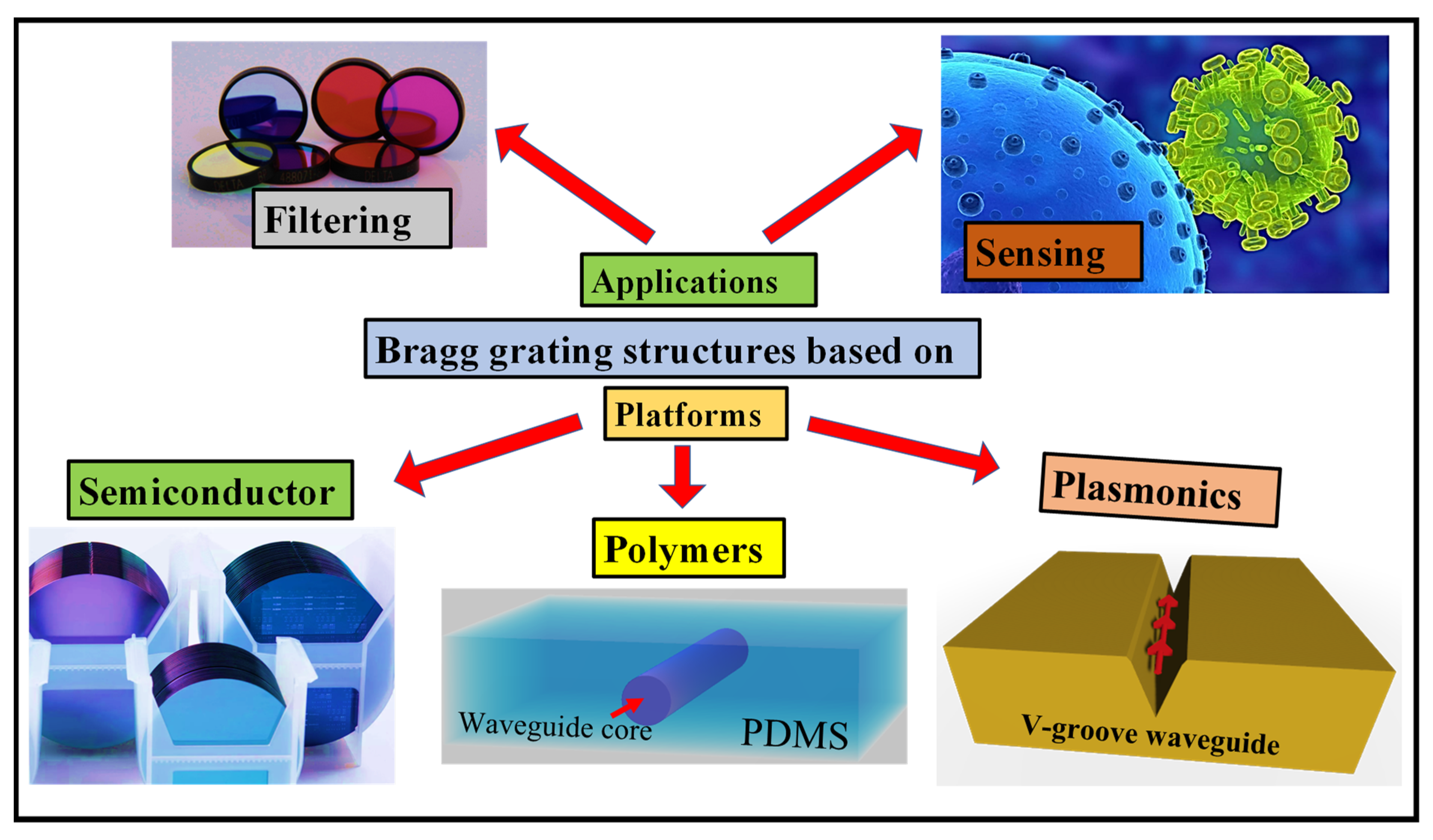
:1. Introduction
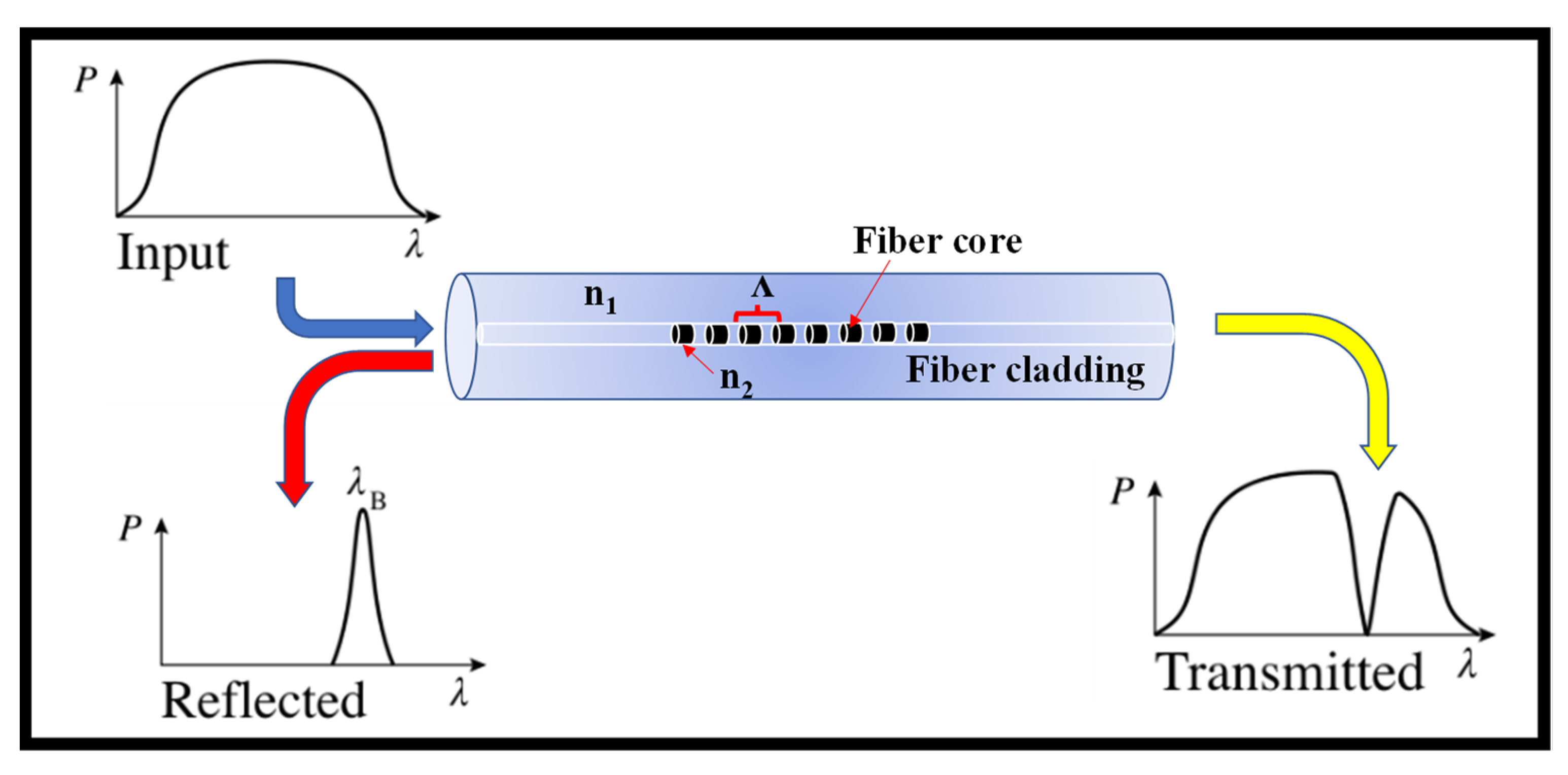
2. Bragg Concept
3. BG Structures Based on a Semiconductor Platform
3.1. Fundamentals of Si-Based BG Structures
3.2. Recent Advances in Si-Based BG Structures
4. BG Structures Based on a Polymer Platform
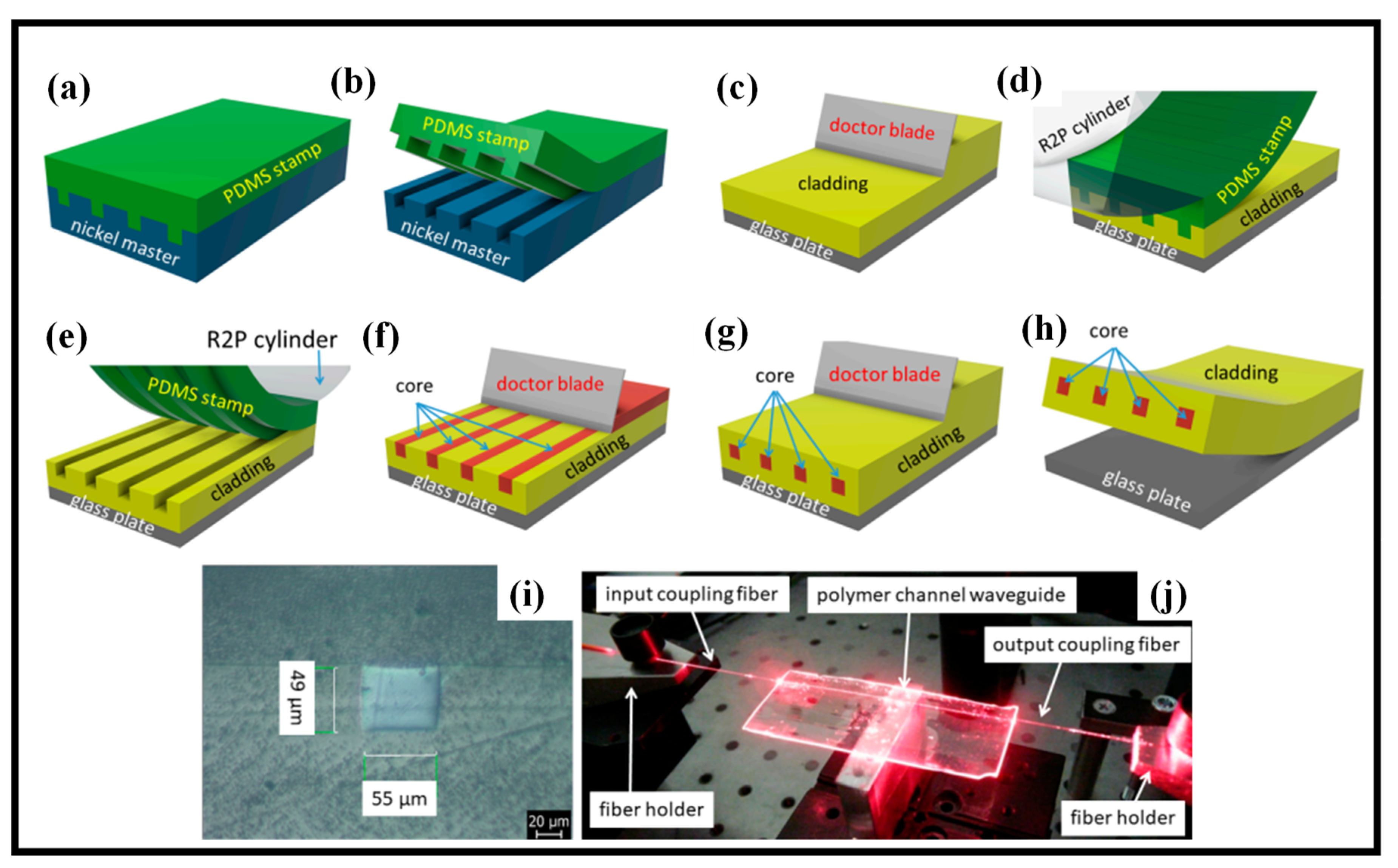
4.1. Polymer Materials and Fabrication Methods
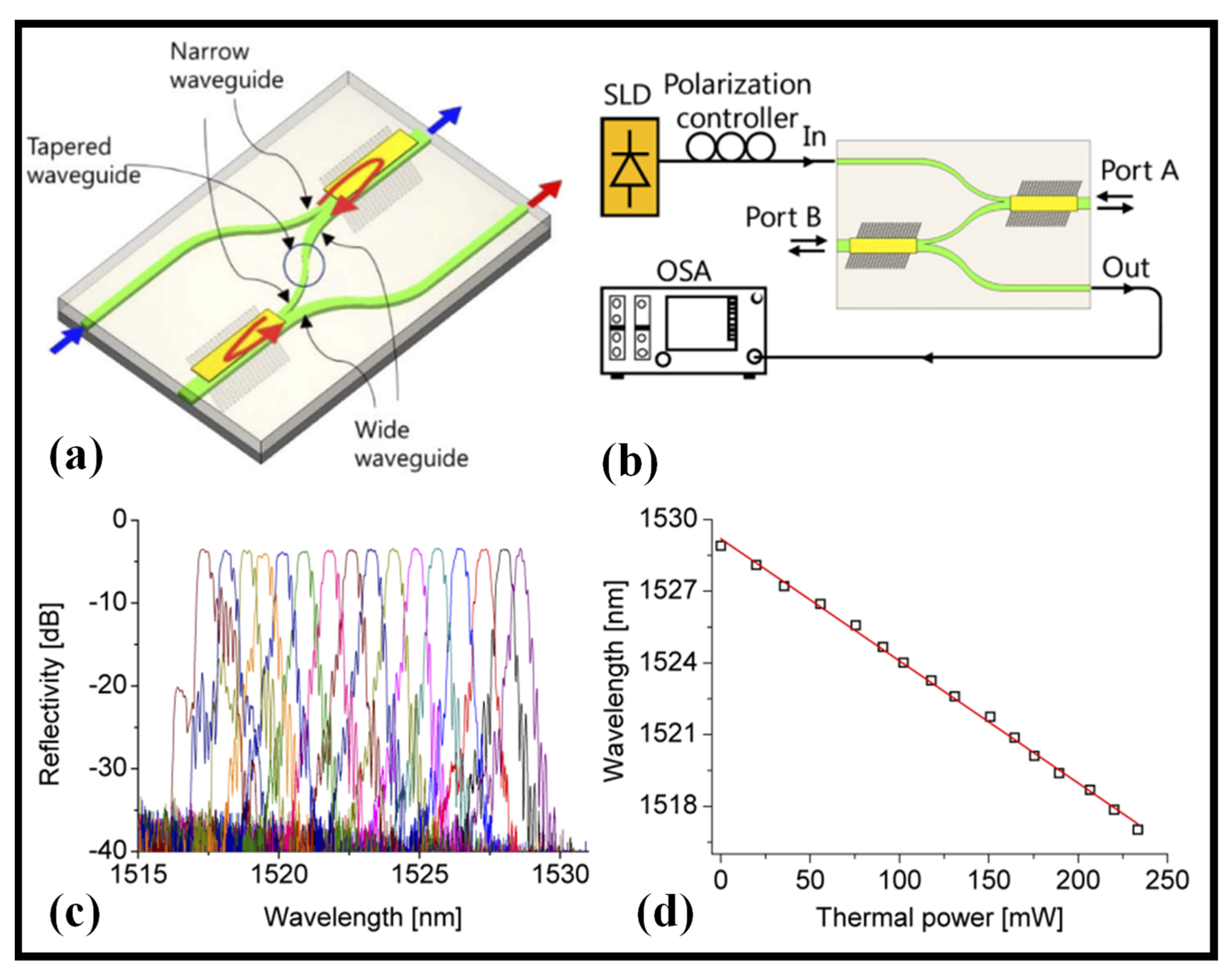
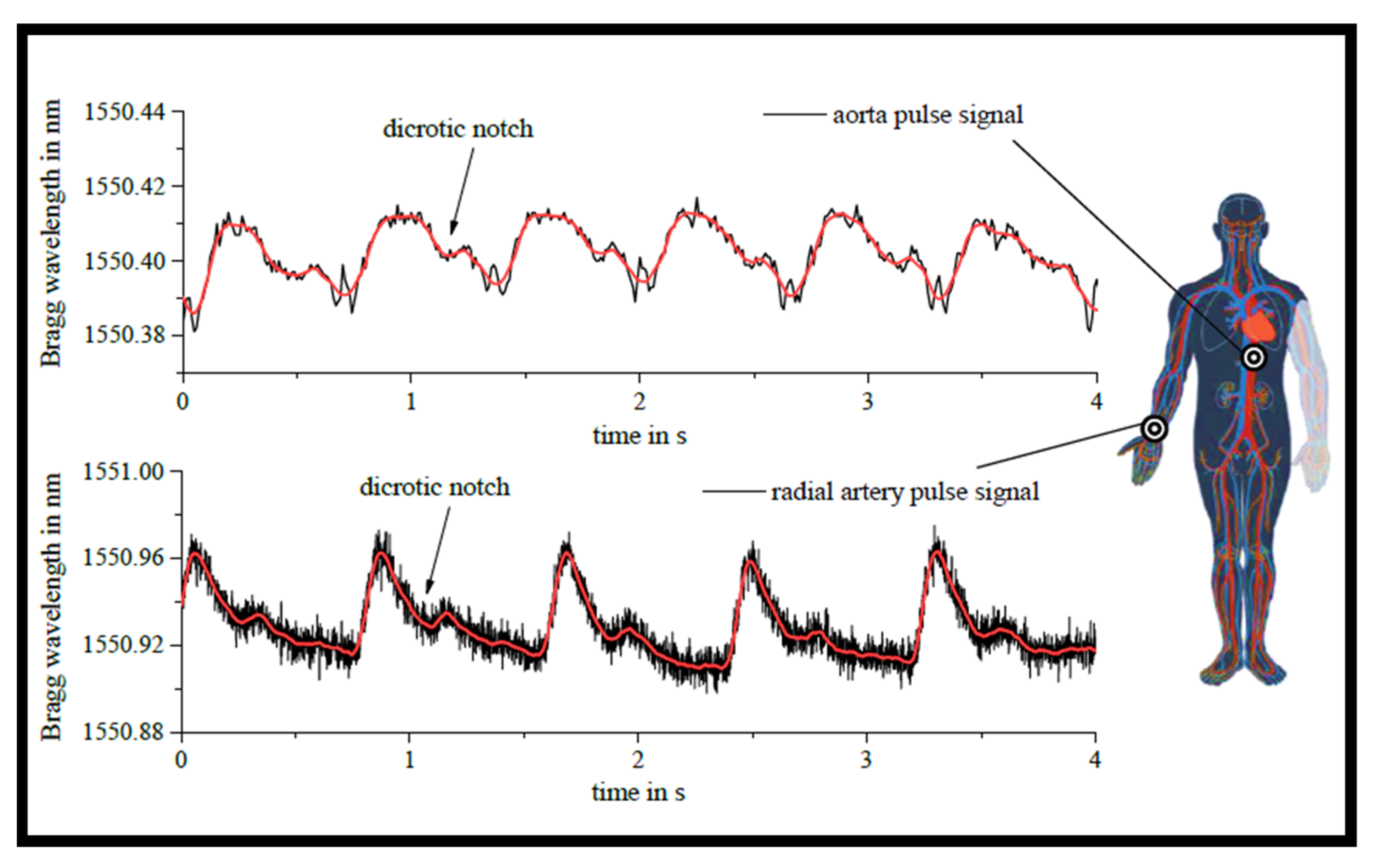
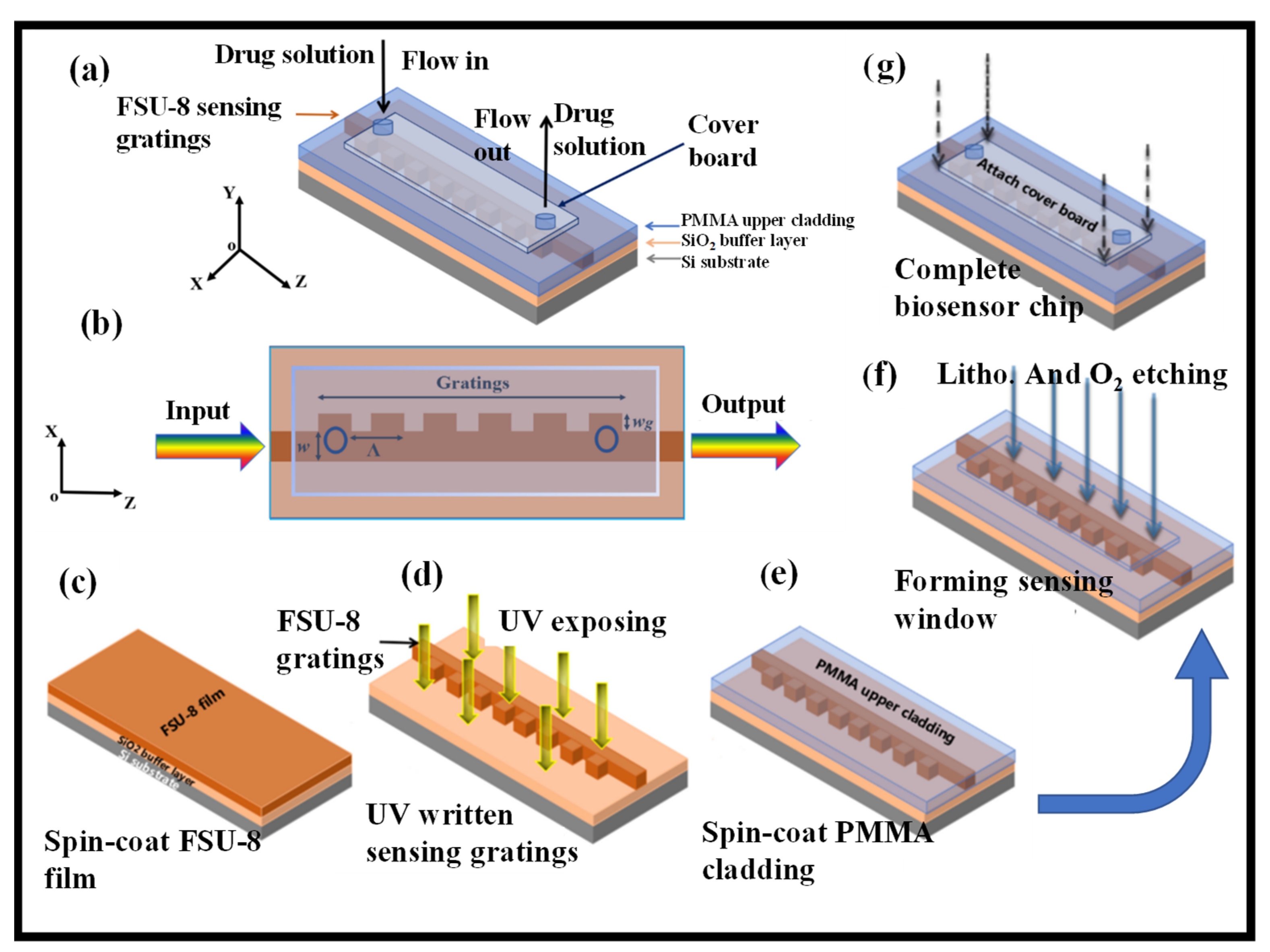
4.2. BGs Based on Polymer Materials as a Filter and Sensing Devices
5. BG Structures Based on the Plasmonic Platform
5.1. Plasmonics Fundamentals and Its Applications
5.2. Types of Plasmonic WGs
5.3. Plasmonic Materials
5.4. Plasmonic BG Filters and Sensors
6. Pros and Cons of the Optical Platforms under Discussion
7. Outlook and Conclusions
Author Contributions
Funding
Institutional Review Board Statement
Informed Consent Statement
Data Availability Statement
Acknowledgments
Conflicts of Interest
Abbreviations
References
- Kazanskiy, N.; Kazmierczak, A.; Butt, M.A. Why slot and hybrid plasmonic waveguides are ideal candidates for sensing applications? Optoelectron. Adv. Mater. Rapid Commun. 2021, 15, 195–206. [Google Scholar]
- Kazanskiy, N.L.; Butt, M.; Khonina, S.N. Silicon photonic devices realized on refractive index engineered subwavelength grating waveguides—A review. Opt. Laser Technol. 2021, 138, 106863. [Google Scholar] [CrossRef]
- Zou, C.; Chang, C.; Sun, D.; Bohringer, K.; Lin, L. Photolithographic patterning of perovskite thin films for multicolor display applications. Nano Lett. 2020, 20, 3710–3717. [Google Scholar] [CrossRef] [PubMed]
- Butt, M.A.; Kazanskiy, N.L.; Khonina, S.N. Label-free detection of ambient refractive index based on plasmonic Bragg gratings embedded resonator cavity sensor. J. Mod. Opt. 2019, 66, 1920–1925. [Google Scholar] [CrossRef]
- Kulishov, M.; Laniel, J.; Belanger, N.; Azana, J.; Plant, D. Nonreciprocal waveguide Bragg gratings. Opt. Express 2005, 13, 3068–3078. [Google Scholar] [CrossRef] [Green Version]
- Hill, K.; Meltz, G. Fiber Bragg grating technology fundamentals and overview. J. Lightwave Technol. 1997, 15, 1263–1276. [Google Scholar] [CrossRef] [Green Version]
- Binfeng, Y.; Guohua, H.; Ruohu, Z.; Yiping, C. Design of a compact and high sensitive refractive index sensor based on metal-insulator-metal plasmonic Bragg grating. Opt. Express 2014, 22, 28662. [Google Scholar] [CrossRef]
- Passaro, V.M.N.; Loiacono, R.; D’Amico, G.; De Leonardis, F. Design of Bragg gratin sensors based on submicrometer optical rib waveguides in SOI. IEEE Sens. J. 2008, 8, 1603–1611. [Google Scholar] [CrossRef]
- Nikolai, N.; Mittal, S.; Berger, M.; Ahmed, Z. On-chip silicon waveguide Bragg grating photonic temperature sensor. Opt. Lett. 2015, 40, 3934–3936. [Google Scholar]
- Hill, K.; Fujii, Y.; Johnson, D.; Kawasaki, B. Photosensitivity in optical fiber waveguides: Application to reflection filter fabrication. Appl. Phys. lett. 1978, 32, 647. [Google Scholar] [CrossRef]
- Kersey, A.D.; Davis, M.A.; Patrick, H.J.; LeBlanc, M.; Koo, K.P.; Askins, C.G.; Putnam, M.A.; Friebele, E.J. Fiber grating sensors. J. Lightwave Technol. 1997, 15, 1442–1463. [Google Scholar] [CrossRef] [Green Version]
- SKhonina, N.; Kazanskiy, N.L.; Butt, M.A. Spectral characteristics of broad band-rejection filter based on Bragg grating, one-dimensional photonic crystal, and subwavelength grating waveguide. Phys. Scr. 2021, 96, 055505. [Google Scholar] [CrossRef]
- Butt, M.; Khonina, S.; Kazanskiy, N. Optical elements based on silicon photonics. Comput. Opt. 2019, 43, 1079–1083. [Google Scholar] [CrossRef]
- Butt, M.A. Numerical investigation of a small footprint plasmonic Bragg grating structure with a high extinction ratio. Photonics Lett. Pol. 2020, 12, 82–84. [Google Scholar] [CrossRef]
- Available online: https://www.okmetic.com/silicon-wafers/soi-wafers-silicon-on-insulator-line/ (accessed on 2 July 2022).
- What Are Optical Bandpass Filters? Available online: https://www.deltaopticalthinfilm.com/what-are-optical-bandpass-filters/ (accessed on 2 July 2022).
- Software-Defined Biosensing: Rapidly Detecting Novel Threats. Available online: https://www.mitre.org/publications/project-stories/softwaredefined-biosensing-rapidly-detecting-novel-threats (accessed on 2 July 2022).
- Bragg, W. The diffraction of short electromagnetic waves by a crystal. Proc. Cambr. Philos. Soc. 1914, 17, 43–57. [Google Scholar]
- Kogelnik, H. Coupled wave theory for thick hologram gratings. Bell Syst. Tech. J. 1969, 48, 2909–2947. [Google Scholar] [CrossRef]
- Butt, M.A.; Khonina, S.N.; Kazanskiy, N.L. Plasmonics: A necessity in the field of sensing-A review (invited). Fiber Integr. Opt. 2021, 40, 14–47. [Google Scholar] [CrossRef]
- Chen, X.; Liu, C.; Hughes, M.; Nagel, D.; Hine, A.; Zhang, L. EDC-mediated oligonucleotide immobilization on a long period grating optical biosensor. J. Biosens. Bioelectron. 2015, 6, 1. [Google Scholar] [CrossRef] [Green Version]
- Chiavaioli, F.; Baldini, F.; Tombelli, S.; Trono, C.; Giannetti, A. Biosensing with optical fiber gratings. Nanophotonics 2017, 6, 663–679. [Google Scholar] [CrossRef]
- Linzi, H.; Wu, Z.; Zhang, X.; Qiangqiang, F.; Jian, X.; Yong, T.; Tuan, G.; Bai-Ou, G. High sensitive thrombin protein detection by plasmonic tilted fiber grating biosensor. In Proceedings of the Workshop on Specialty Optical Fibers and Their Applications, Hong Kong, China, 4–6 November 2015. [Google Scholar]
- Coelho, L.; de Almeida, J.M.; Santos, J.; Jorge, P.; Martins, M.; Viegas, D.; Queiros, R. Aptamer-based fiber sensor for thrombin detection. J. Biomed. Opt. 2016, 21, 087005. [Google Scholar] [CrossRef]
- Arghir, I.; Spasic, D.; Verlinden, B.; Delport, F.; Lammertyn, J. Improved surface plasmon resonance biosensing using silanized optical fibers. Sens. Actuators B Chem. 2015, 216, 518–526. [Google Scholar] [CrossRef] [Green Version]
- Bragg, W.; Bragg, W. The reflection of X-rays by crystals. R. Soc. Lond. Proc. Ser. A 1913, 88, 428–438. [Google Scholar] [CrossRef]
- Rahim, A.; Goyvaerts, J.; Szelag, B.; Fedeli, J.-M.; Absil, P.; Aalto, T.; Harjanne, M.; Littlejohns, C.G.; Reed, G.T.; Winzer, G.; et al. Open-access silicon photonics platforms in Europe. IEEE J. Sel. Top. Quantum Electron. 2019, 25, 1–18. [Google Scholar] [CrossRef] [Green Version]
- Giewont, K.; Hu, S.; Peng, B.; Rakowski, M.; Rauch, S.; Rosenberg, J.C.; Sahin, A.; Stobert, I.; Stricker, A.; Nummy, K.; et al. 300-mm monolithic silicon photonics foundry technology. IEEE J. Sel. Top. Quantum Electron. 2019, 25, 1–11. [Google Scholar] [CrossRef]
- Sorace-Agaskar, C.; Kharas, D.; Yegnanarayanan, S.; Maxson, R.T.; West, G.N.; Loh, W.; Bramhavar, S.; Ram, R.J.; Chiaverini, J.; Sage, J.; et al. Versatile silicon nitride and alumina integrated photonic platforms for the ultraviolet to short-wave infrared. IEEE J. Sel. Top. Quantum Electron. 2019, 25, 1–15. [Google Scholar] [CrossRef]
- Fahrenkopf, N.; McDonough, C.; Leake, G.; Su, Z.; Timurdogan, E.; Coolbaugh, D. The AIM photonics MPW: A highly accessible cutting edge technology for rapid prototyping of photonic integrated circuits. IEEE J. Sel. Top. Quantum Electron. 2019, 25, 1–6. [Google Scholar] [CrossRef]
- Coldren, L.; Corzine, S.; Masanovic, M. Diode Lasers Ad Photonic Integrated Circuits, 2nd ed.; John Wiley & Sons: Hoboken, NJ, USA, 2012. [Google Scholar]
- Leinse, A.; Heideman, R.G.; Hoekman, M.; Schreuder, F.; Falke, F.; Roeloffzen, C.G.H.; Zhuang, L.; Burla, M.; Marpaung, D.; Geuzebroek, D.H.; et al. TripleX waveguide platform: Low-loss technology over a wide wavelength range. SPIE Microtechnologies Integr. Photonics Mater. Devices Appl. II 2013, 8767, 86–98. [Google Scholar]
- Gao, G.; Zhang, Y.; Zhang, H.; Wang, Y.; Huang, Q.; Xia, J. Air-mode photonic crystal ring resonator on silicon-on-insulator. Sci. Rep. 2016, 6, 19999. [Google Scholar] [CrossRef]
- Belt, M.; Bovington, J.; Moreira, R.; Bauters, J.; Heck, M.; Barton, J.; Bowers, J.; Blumenthal, D. Sidewall gratings in ultra-low-loss Si3N4 planar waveguides. Optics Express 2013, 21, 1181–1188. [Google Scholar] [CrossRef] [Green Version]
- Carras, M.; Garcia, M.; Marcadet, X.; Parillaud, O.; Rossi, A.; Bansropun, S. Top grating index-coupled distributed feedback quantum cascade lasers. Appl. Phys. Lett. 2008, 93, 011109. [Google Scholar] [CrossRef]
- Wang, X.; Shi, W.; Vafaei, R.; Jaeger, N.; Chrostowski, L. Uniform and sampled Bragg gratings in SOI strip waveguides with sidewall corrugations. IEEE Photonics Technol. Lett. 2011, 23, 290–292. [Google Scholar] [CrossRef]
- Spencer, D.; Davenport, M.; Srinivasan, S.; Khurgin, J.; Morton, P.; Bowers, J. Low kappa, narrow bandwidth Si3N4 Bragg gratings. Opt. Express 2015, 23, 30329. [Google Scholar] [CrossRef] [PubMed]
- Chrostowski, L.; Hochberg, M. Silicon Photonics Design from Devices to Systems, 1st ed.; Cambridge University: Cambridge, UK, 2015. [Google Scholar]
- Santis, C.; Steger, S.; Vilenchik, Y.; Vasilyev, A.; Yariv, A. High-coherence semiconductor lasers based on integral high-Q resonators in hybrid Si/III-V platforms. Proc. Natl. Acad. Sci. USA 2014, 111, 2879–2884. [Google Scholar] [CrossRef] [Green Version]
- Xiang, C.; Morton, P.; Bowers, J. Ultra-narrow linewidth laser based on a semiconductor gain chip and extended Si3N4 Bragg grating. Opt. Lett. 2019, 44, 3825. [Google Scholar] [CrossRef] [PubMed]
- Sakai, A.; Hara, G.; Baba, T. Propagation characteristics of ultrahigh—delta optical waveguide on silicon-on-insulator substrate. Jpn. J. Appl. Phys. Part 2 2001, 40, L383. [Google Scholar] [CrossRef] [Green Version]
- Utaka, K.; Akiba, S.; Sakai, K.; Matsushima, Y. Lambda-4 shifted InGaAsP/InP DFB lasers. IEEE J. Quantum Electron. 1986, 22, 1042–1051. [Google Scholar] [CrossRef]
- Husko, C.; Ducharme, A.; Fahrenkopf, N.; Guest, J. Phase-shifted Bragg gratings in a foundry silicon nitride platform. OSA Contin. 2021, 4, 933. [Google Scholar] [CrossRef]
- Zhang, W.; Yao, J. A fully reconfigurable waveguide Bragg grating for programmable photonic signal processing. Nat. Commun. 2018, 9, 1396. [Google Scholar] [CrossRef]
- Ciminelli, C.; Dell’Olio, F.; Brunetti, G.; Contedura, D.; Armenise, M. New microwave photonic filter based on a ring resonator including a photonic crystal structure. In Proceedings of the 19th International Conference on Transparent Optical Networks (ICTON), Girona, Spain, 2–6 July 2017; pp. 1–4. [Google Scholar]
- Ciminelli, C.; Innone, F.; Brunetti, G. Rigorous model for the design of ultra-high Q-factor resonant cavities. In Proceedings of the 2016 18th International Conference on Transparent Optical Networks (ICTON), Trento, Italy, 10–14 July 2016; pp. 1–4. [Google Scholar]
- Feced, R.; Zervas, M.; Muriel, M. Efficient inverse scattering algorithm for the design of nonuniform fiber Bragg gratings. IEEE J. Quantum Electron. 1999, 35, 1105–1115. [Google Scholar] [CrossRef]
- Simard, A.; Strain, M.; Meriggi, L.; Sorel, M.; LaRochelle, S. Bandpass integrated Bragg gratings in silicon-on-insulator with well-controlled amplitude and phase responses. Opt. Lett. 2015, 40, 736–739. [Google Scholar] [CrossRef] [Green Version]
- Wang, J.; Chen, L. Low crosstalk Bragg grating/Mach-Zehnder interferometer optical add-drop multiplexer in silicon photonics. Opt. Express 2015, 23, 26450–26459. [Google Scholar] [CrossRef] [PubMed]
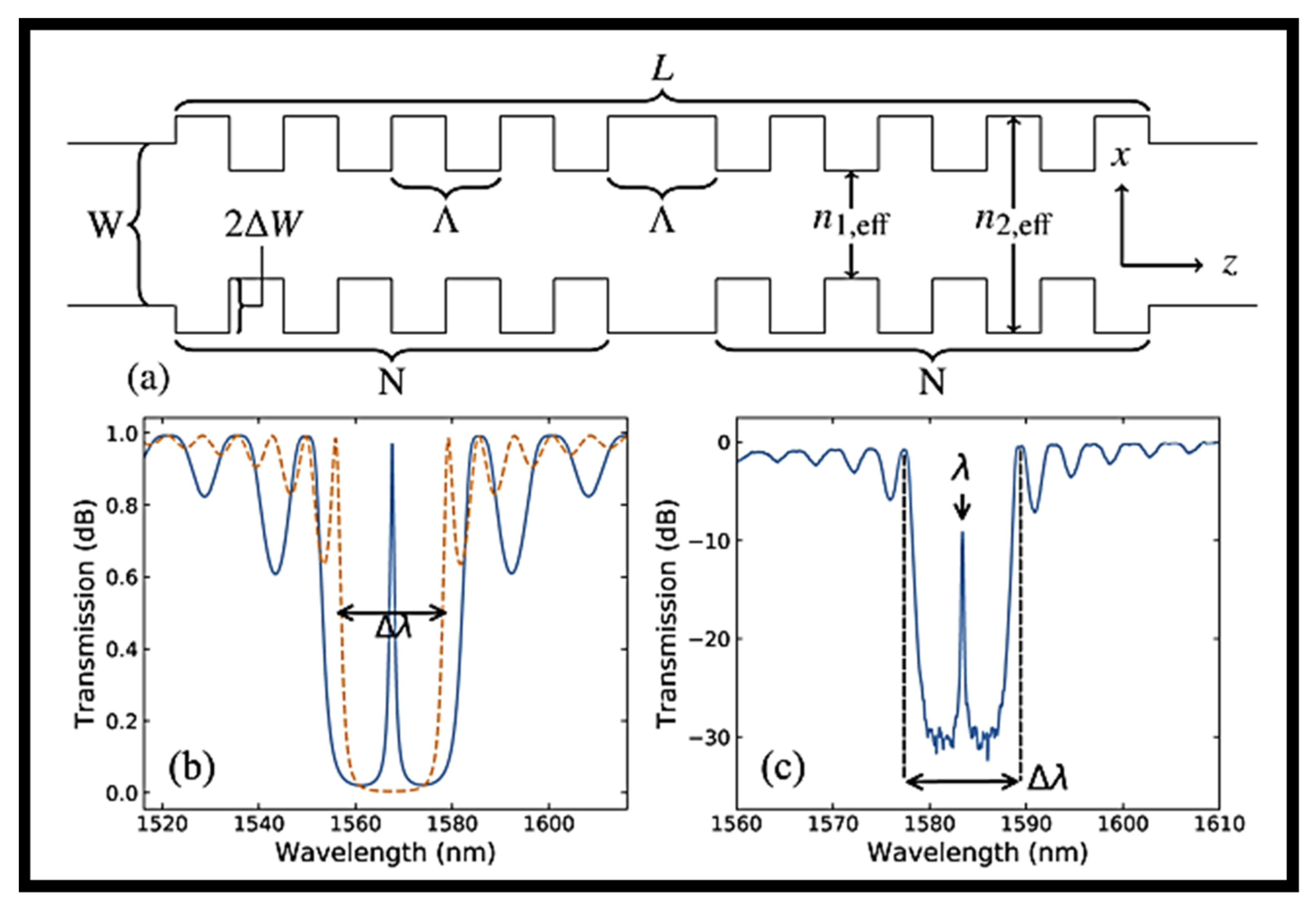
- Kaushal, S.; Cheng, R.; Ma, M.; Mistry, A.; Burla, M.; Chrostowski, L.; Azana, J. Optical signal processing based on silicon photonics waveguide Bragg gratings: Review. Front. Optoelectron. 2018, 11, 163–188. [Google Scholar] [CrossRef]
- Cheng, R.; Jaeger, N.; Chrostowski, L. Fully tailored integrated-optic resonators based on chirped waveguide Moire gratings. Optica 2020, 7, 647–657. [Google Scholar] [CrossRef]
- Hu, Y.; Xie, S.; Zhan, J.; Zhang, Y.; Veilleux, S.; Dagenais, M. Integrated Arbitrary filter with spiral gratings: Design and characterization. J. Lightwave Technol. 2020, 38, 4454–4461. [Google Scholar] [CrossRef]
- Simard, A.; Belhadj, N.; Painchaud, Y.; LaRochelle, S. Apodized Silicon-on-Insulator Bragg Gratings. IEEE Photonics Technol. Lett. 2012, 24, 1033–1035. [Google Scholar] [CrossRef]
- Bazargani, H.; Burla, M.; Chrostowski, L.; Azana, J. Photonic Hilbert transformer based on laterally apodized integrated waveguide Bragg gratings on a SOI wafer. Opt. Lett. 2016, 41, 5039–5042. [Google Scholar] [CrossRef] [PubMed]
- Cheng, R.; Chrostowski, L. Multichannel photonic Hilbert transformers based on complex modulated integrated Bragg gratings. Opt. Lett. 2018, 43, 1031–1034. [Google Scholar] [CrossRef]
- Cheng, R.; Chrostowski, L. Apodization of silicon integrated Bragg gratings through periodic phase modulation. IEEE J. Sel. Top. Quantum Electron. 2019, 25, 1–15. [Google Scholar] [CrossRef]
- Zamek, S.; Tan, D.; Khajavikhan, M.; Ayache, M.; Nezhad, M.; Fainman, Y. Compact chip-scale filter based on curved waveguide Bragg gratings. Opt. Lett. 2010, 35, 3477–3479. [Google Scholar] [CrossRef] [Green Version]
- Hung, Y.-J.; Lin, K.-H.; Wu, C.-J.; Wang, C.-Y.; Chen, Y.-J. Narrowband reflection from weakly coupled cladding-modulated Bragg gratings. IEEE J. Sel. Top. Quantum Electron. 2016, 22, 218–224. [Google Scholar] [CrossRef]
- Qiu, H.; Lin, L.; Yu, P.; Dai, T.; Jiang, X.; Yu, H. Narrow-band add-drop filter based on cladding-modulated apodized multimode Bragg grating. J. Lightwave Technol. 2019, 37, 5542–5547. [Google Scholar] [CrossRef]
- Yen, T.-H.; Hung, Y.-J. Narrowband Dual-wavelength silicon waveguide Bragg reflectors. J. Lightwave Technol. 2019, 37, 5326–5332. [Google Scholar] [CrossRef]
- Pereira-Martin, D.; Luque-Gonzalez, J.M.; Wangüemert-Pérez, J.G.; Hadij-ElHouati, A.; Molina-Fernández, Í.; Cheben, P.; Schmid, J.H.; Wang, S.; Ye, W.N.; Čtyroký, J.; et al. Complex spectral filters in silicon waveguides based on cladding-modulated Bragg gratings. Opt. Express 2021, 29, 15867. [Google Scholar] [CrossRef] [PubMed]
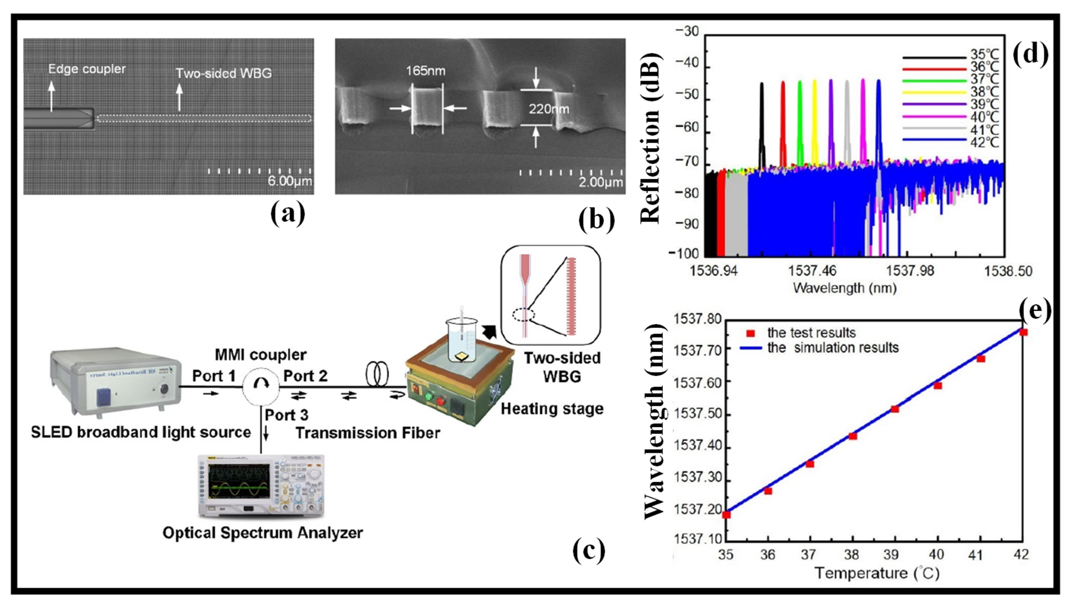
- Li, H.; An, Z.; Mao, Q.; Zuo, S.; Zhu, W.; Zhang, S.; Zhang, C.; Li, E.; Garcia, J. SOI waveguide Bragg grating photonic sensor for human body temperature measurement based on photonic integrated interrogator. Nanomaterials 2022, 12, 29. [Google Scholar] [CrossRef]
- Groh, W. Overtone absorption in macromolecules for polymer optical fibers. Die Makromol. Chem. 1988, 189, 2861–2874. [Google Scholar] [CrossRef]
- Oh, M.-C.; Kim, K.-J.; Chu, W.-S.; Kim, J.-W.; Seo, J.-K.; Noh, Y.-O.; Lee, H.-J. Integrated photonic devices incorporating low-loss fluorinated polymer materials. Polymers 2011, 3, 975–997. [Google Scholar] [CrossRef] [Green Version]
- Yeniay, A.; Gao, R.; Takayama, K.; Gao, R.; Garito, A. Ultra-low-loss polymer waveguides. J. Lightwave Technol. 2004, 22, 154–158. [Google Scholar] [CrossRef]
- Babudri, F.; Farinola, G.; Naso, F.; Raqni, R. Fluorinated organic materials for electronic and optoelectronic applications: The role of the fluorine atom. Chem. Commun. 2007, 10, 1003–1022. [Google Scholar] [CrossRef]
- Lee, H.-J.; Lee, E.-M.; Lee, M.-H.; Oh, M.-C.; Ahn, J.-H.; Han, S.G.; Kim, H.G. Crosslinkable fluorinated poly(arylene ethers) bearing phenyl ethynyl moiety for low-loss polymer optical waveguide devices. J. Polym. Sci. Part A Polym. Chem. 1998, 36, 2881–2887. [Google Scholar] [CrossRef]
- Noh, Y.-O.; Lee, C.-H.; Kim, J.-M.; Hwang, W.-Y.; Oh, M.-C.; Won, Y.-H.; Lee, H.-J.; Han, S.-G. Polymer waveguide variable optical attenuator and its reliability. Opt. Commun. 2004, 242, 533–540. [Google Scholar] [CrossRef]
- Ma, H.; Jen, A.-Y.; Dalton, L. Polymer-based optical waveguides:materials, processing, and devices. Adv. Mater. 2002, 14, 1339–1365. [Google Scholar] [CrossRef]
- Prajzler, V.; Hyps, P.; Mastera, R.; Nekvindova, P. Properties of Siloxane based optical waveguides deposited on transparent paper and foil. Radioengineering 2016, 25, 230–235. [Google Scholar] [CrossRef]
- Beche, B.; Pelletier, N.; Gaviot, E.; Zyss, J. Single-mode TE00-TM00 optical waveguides on SU-8 polymer. Opt. Commun. 2004, 230, 91–94. [Google Scholar] [CrossRef]
- Prajzler, V.; Neruda, M.; Jasek, P.; Nekvindova, P. The properties of free-standing epoxy polymer multi-mode optical waveguides. Microsyst. Technol. 2019, 25, 257–264. [Google Scholar] [CrossRef]
- Ibrahim, M.; Kassim, N.; Mohammad, A.; Lee, S.-Y.; Chin, M.-K. Single mode optical waveguides based on photodefinable benzocyclobutene (BCB 4024-40) polymer. Microw. Opt. Lett. 2006, 49, 479–481. [Google Scholar] [CrossRef]
- Chemoptics Inc. Available online: https://www.chemoptics.co.kr/en/ (accessed on 2 July 2022).
- Prajzler, V.; Jasek, P.; Nekvindova, P. Inorganic-organic hybrid polymer optical planar waveguides for micro-opto-electro-mechanical systems (MOEMS). Microsyst. Technol. 2019, 25, 2249–2258. [Google Scholar] [CrossRef]
- Available online: https://www.microresist.de/en/produkt/ormoclearfx/ (accessed on 2 July 2022).
- Cai, Z.; Qiu, W.; Shao, G.; Wang, W. A new fabrication method for all-PDMS waveguides. Sens. Actuators A Phys. 2013, 204, 44–47. [Google Scholar] [CrossRef]
- Prajzler, V.; Neruda, M.; Nekvindova, P. Flexible multimode polydimethyl-diphenylsiloxane optical planar waveguides. J. Mater. Sci. Mater. Electron. 2018, 29, 5878–5884. [Google Scholar] [CrossRef]
- Buestrich, R.; Kahlenberg, F.; Popall, M.; Dannberg, P.; Muller-Fiedler, R.; Rosch, O. ORMOCER (R) s for optical interconnection technology. J. Sol-Gel Sci. Technol. 2001, 20, 181–186. [Google Scholar] [CrossRef]
- Bosman, E.; van Steenberge, G.; Christiaens, W.; Hendrickx, N.; Vanfleteren, J.; van Daele, P. Active optical links embedded in flexible substrates. In Proceedings of the 58th Electronic Components and Technology Conference, Lake Buena Vista, FL, USA, 27–30 May 2008; pp. 1150–1157. [Google Scholar]
- Bamiedakis, N.; Beals, J.; Penty, R.; White, I.; DeGroot, J.; Clapp, T. Cost-effective multimode polymer waveguides for high-speed on-board optical interconnects. IEEE J. Quantum Electron. 2009, 45, 415–424. [Google Scholar] [CrossRef]
- Kagami, M.; Kawasaki, A.; Ito, H. A polymer optical waveguide with out-of-plane branching mirrors for surface-normal optical interconnections. J. Lightwave Technol. 2001, 19, 1949–1955. [Google Scholar] [CrossRef]
- Klein, S.; Barsella, A.; Leblond, H.; Bulou, H.; Fort, A.; Andraud, C.; Lemercier, G.; Mulatier, J.C.; Dorkenoo, K. One-step waveguide and optical circuit writing in photopolymerizable materials processed by two-photon absorption. Appl. Phys. Lett. 2005, 86, 211118. [Google Scholar] [CrossRef]
- Elmogi, A.; Bosman, E.; Missinne, J.; Van, G.S. Comparison of epoxy- and siloxane-based single-mode optical waveguides defined by direct-write lithography. Opt. Mater. 2016, 52, 26–31. [Google Scholar] [CrossRef]
- Wong, W.; Zhou, J.; Pun, E. Low-loss polymeric optical waveguides using electron-beam direct writing. Appl. Phys. Lett. 2001, 78, 2110–2112. [Google Scholar] [CrossRef]
- Wolfer, T.; Bollgruen, P.; Mager, D.; Overmeyer, L.; Korvink, J. Flexographic and inkjet printing of polymer optical waveguides for fully integrated sensor system. Procedia Technol. 2014, 15, 521–529. [Google Scholar] [CrossRef] [Green Version]
- Choi, C.-G.; Han, S.-P.; Kim, B.; Ahn, S.-H.; Jeong, M.-Y. Fabrication of large-core 1x16 optical power splitters in polymers using hot-embossing process. IEEE Photon. Technol. Lett. 2003, 15, 825–827. [Google Scholar] [CrossRef]
- Fan, R.; Hooker, R. Tapered polymer single-mode waveguides for mode transformation. J. Lightwave Technol. 1999, 17, 466–474. [Google Scholar] [CrossRef]
- Kooy, N.; Mohamed, K.; Pin, L.; Guan, O. A review of roll-to-roll nanoimprint lithography. Nanoscale Res. Lett. 2014, 9, 320. [Google Scholar] [CrossRef] [Green Version]
- Ahn, S.; Guo, L. Large-area roll-to-roll and roll-to-plate nanoimprint lithography: A step toward high-throughput application of continuous nanoimprinting. ACS Nano 2009, 3, 2304–2310. [Google Scholar] [CrossRef]
- Prajzler, V.; Chlupaty, V.; Kulha, P.; Neruda, M.; Kopp, S.; Mujlberger, M. Optical Polymer Waveguides Fabricated by Roll-to-Plate nanoimprinting technique. Nanomaterials 2021, 11, 724. [Google Scholar] [CrossRef]
- Zhou, J.; Wong, W.; Pun, E.; Shen, Y.; Zhao, Y. Fabrication of low loss optical waveguides with a novel thermo-optical polymer material. Opt. Appl. 2006, 36, 429. [Google Scholar]
- Park, T.-H.; Shin, J.-S.; Huang, G.; Chu, W.-S.; Oh, M.-C. Tunable channel drop filters consisting of a tilted Bragg grating and a mode sorting polymer waveguide. Opt. Express 2016, 24, 5709. [Google Scholar] [CrossRef] [PubMed]
- Wong, W.; Pun, E.; Chan, K. Electron beam direct-write tunable polymeric waveguide grating filter. IEEE Photon. Technol. Lett. 2003, 15, 1731–1733. [Google Scholar] [CrossRef]
- Zhu, L.; Huang, Y.; Green, W.; Yariv, A. Tunable transmission filters based on corrugrated sidewall Bragg gratings in polymer waveguides. In Proceedings of the Conference on Lasers and Electro-Optics, Optical Society of America, Baltimore, MD, USA, 22–27 May 2005. [Google Scholar]
- Liu, A.; Zhang, Z.; de Felipe, D.; Keil, N.; Grote, N. Power-efficient thermo-optic tunable filters based on polymeric waveguide Bragg gratings. IEEE Photon. Technol. Lett. 2014, 26, 313–315. [Google Scholar] [CrossRef]
- Zhang, Z.; Maese-Novo, A.; Schwartz, E.; Zawadzki, C.; Keil, N. 301-nm wavelength tunable differentially driven all-polymer optical filter. Opt. Lett. 2014, 39, 5170–5172. [Google Scholar] [CrossRef] [PubMed]
- Eldada, L.; Blomquist, R.; Maxfield, M.; Pant, D. Thermooptic planar polymer Bragg grating OADM’s with broad tuning range. IEEE Photon. Technol. Lett. 1999, 11, 448–450. [Google Scholar] [CrossRef]
- Katebi-Jahromi, A.; Karimi-Alavijeh, H.; Jalilpiran, S.; Arianfard, H.; Gharavi, A. Integrated 1x2 polymeric add/drop multiplexer. J. Lightwave Technol. 2012, 30, 700–703. [Google Scholar] [CrossRef]
- Wang, L.; Li, Y.; Porcel, M.; Vermeulen, D.; Han, X.; Wang, J.; Jian, X.; Baets, R.; Zhao, R.; Morthier, G. A polymer-based surface grating coupler with an embedded Si3N4 layer. J. Appl. Phys. 2012, 111, 114507. [Google Scholar] [CrossRef] [Green Version]
- Yang, Y.; Chen, K.; Jin, W.; Chiang, K. Mode converter with polymer long-period waveguide grating. In Proceedings of the Asia Communications and Photonics Conference Optical Society of America, Shanghai, China, 11–14 November 2014; p. 4. [Google Scholar]
- Mizunami, T.; Djambova, T.; Niiho, T.; Gupta, S. Bragg gratings in multimode and few-mode optical fibers. J. Lightwave Technol. 2000, 18, 230. [Google Scholar] [CrossRef]
- Zhang, Z.; Tao, X. Intrinsic temperature sensitivity of fiber Bragg gratings in PMMA-based optical fibers. IEEE Photon. Technol. Lett. 2013, 25, 310–312. [Google Scholar] [CrossRef]
- Rosenberger, M.; Hessler, S.; Belle, S.; Schmauss, B.; Hellmann, R. Compressive and tensile strain sensing using a polymer planar Bragg grating. Opt. Express 2014, 22, 5483–5490. [Google Scholar] [CrossRef] [PubMed]
- Felipe, D.; Zhang, Z.; Brinker, W.; Kleinert, M.; Novo, A.M.; Zawadzki, C.; Moehrle, M.; Keil, N. Polymer-based external cavity lasers: Tuning efficiency, reliability and polarization diversity. IEEE Photon. Technol. Lett. 2014, 26, 1391–1394. [Google Scholar] [CrossRef]
- Oh, S.-H.; Yoon, K.-H.; Kim, K.-S.; Kwon, O.-K.; Oh, D.-K.; Noh, Y.-O.; Seo, J.-K.; Lee, H.-J. Tunable external cavity laser by hybrid integration of a super-luminescent diode and a polymer Bragg reflector. IEEE J. Sel. Topics Quantum Electron. 2011, 17, 1534–1541. [Google Scholar]
- Park, T.-H.; Kim, S.-M.; Oh, M.-C. Polymeric tunable wavelength filter with two-stage cascaded tilted Bragg gratings. Opt. Express 2020, 28, 10145–10152. [Google Scholar] [CrossRef] [PubMed]
- Cerrina, F. X-ray imaging: Applications to patterning and lithography. J. Phys. D Appl. Phys. 2000, 33, R103–R116. [Google Scholar] [CrossRef]
- Kolodziej, C.; Maynard, H. Electron-beam lithography for patterning biomolecules at the micron and nanometer scale. Chem. Mater. 2012, 24, 774–780. [Google Scholar] [CrossRef]
- Schift, H.; Kristensen, A. Nanoimprint Lithography-Patterning of Resists Using Molding; Bhushan, B., Ed.; Springer Handbook of Nanotechnology: Berlin/Heidelberg, Germany, 2010. [Google Scholar]
- Jonusauskas, L.; Andrijec, D.; Andriukaitis, D.; Vargalis, R.; Baravykas, T.; Stankevičius, A.; Merkininkaite, G.; Pautienius, A.; Gricius, H.; Ežerskyte, E.; et al. Expansion of direct laser writing (DLW) capabilities for usage in biomedical applications. Laser 3d Manuf. VIII 2021, 11677, 73–84. [Google Scholar]
- Missinne, J.; Vasiliev, A.; Elmogi, A.; Beneitez, N.; Bosman, E.; Hoe, B.; Steenberge, G. Bragg grating sensors in laser-written single mode polymer waveguides. Procedia Eng. 2015, 120, 878–881. [Google Scholar] [CrossRef]
- Mares, D.; Jerabek, V. Polymer waveguide Bragg gratings made by laser patterning technique. Opt. Quantum Electron. 2016, 48, 158. [Google Scholar] [CrossRef]
- Hessler, S.; Bott, P.; Kefer, S.; Schmauss, B.; Hellmann, R. Multipurpose Polymer Bragg Grating-based optomechanical sensor pad. Sensors 2019, 19, 4101. [Google Scholar] [CrossRef] [Green Version]
- Wang, C.; Yi, P.; Li, J.; Dong, H.; Chen, C.; Zhang, D.; Shen, H.; Fu, B. Polymer optical waveguide grating-based biosensor to detect effective drug concentrations of Ginkgolide A for inhibition of PMVEC apoptosis. Biosensors 2021, 11, 264. [Google Scholar] [CrossRef] [PubMed]
- Kazanskiy, N.L.; Khonina, S.N.; Butt, M.A. Plasmonic sensors based on Metal-insulator-Metal waveguides for refractive index sensing applications: A brief review. Phys. E Low-Dimens. Syst. Nanostruct. 2020, 117, 113798. [Google Scholar] [CrossRef]
- Kazanskiy, N.L.; Butt, M.A.; Degtyarev, S.A.; Khonina, S.N. Achievements in the development of plasmonic waveguide sensors for measuring the refractive index. Comput. Opt. 2020, 44, 295–318. [Google Scholar] [CrossRef]
- Giannini, V.; Fernandez-Dominguez, A.; Heck, S.; Maier, S. Plasmonic nanoantennas: Fundamentals and their use in controlling the radiative properties of nanoemitters. Chem. Rev. 2011, 111, 3888–3912. [Google Scholar] [CrossRef] [PubMed]
- Tseng, S.-Y.; Li, S.-Y.; Yi, S.-Y.; Sun, A.Y.; Gao, D.-Y.; Wan, D. Food quality monitor: Paper-based plasmonic sensors prepared through reversal nanoimprinting for rapid detection of biogenic amine odorants. ACS Appl. Mater. Interfaces 2017, 9, 17306–17316. [Google Scholar] [CrossRef]
- Thenmozhi, H.; Rajan, M.; Ahmed, K. D-shaped PCF sensor based on SPR for the detection of carcinogenic agents in food and cosmetics. Optik 2019, 180, 264–270. [Google Scholar] [CrossRef]
- Ameen, A.; Gartia, M.R.; Hsiao, A. Ultra-sensitive colorimetric plasmonic sensing and microfluidics for biofluid diagnostics using nanohole array. J. Nanomater. 2015, 2015, 460895. [Google Scholar] [CrossRef]
- Ahmed, K.; Haque, M.J.; Jabin, M.A.; Paul, B.K.; Amiri, I.S.; Yupapin, P. Tetra-core surface plasmon resnance based biosensor for alcohol sensing. Phys. B Condens. Matter 2019, 570, 48–52. [Google Scholar] [CrossRef]
- Ahmed, K.; Jabin, M.; Paul, B. Surface plasmon resonance-based gold-coated biosensor for the detection of fuel adulteration. J. Comput. Electron. 2020, 19, 321–332. [Google Scholar] [CrossRef]
- Bellassai, N.; D’Agata, R.; Jungbluth, V.; Spoto, G. Surface plasmon resonance for biomarker detection: Advances in non-invasive cancer diagnosis. Front. Chem. 2019, 7, 570. [Google Scholar] [CrossRef] [Green Version]
- Jabin, M.A.; Luo, Y.; Peng, G.-D.; Rana, G.; Ahmed, K.; Nguyen, T.K.; Paul, B.K.; Dhasarathan, V. Design and fabrication of amoeba faced photonic crystal fiber for biosensing application. Sens. Actuators A Phys. 2020, 313, 112204. [Google Scholar] [CrossRef]
- Ahmed, K.; Paul, B.K.; Vasudevan, B.; Rashed, A.N.Z.; Maheswar, R.; Amiri, I.; Yupapin, P. Design of D-shaped elliptical core photonic crystal fiber for blood plasma cell sensing application. Results Phys. 2019, 12, 2021–2025. [Google Scholar] [CrossRef]
- Mitu, S.A.; Ahmed, K.; Al Zahrani, F.A.; Grover, A.; Rajan, M.S.M.; Moni, M.A. Development and analysis of surface plasmon resonance based refractive index sensor for pregnancy testing. Opt. Lasers Eng. 2021, 140, 106551. [Google Scholar] [CrossRef]
- Vo-Dinh, T.; Wang, H.-N.; Scaffidi, J. Plasmonic nanoprobes for SERS biosensing and bioimaging. J. Biophotonics 2010, 3, 89–102. [Google Scholar] [CrossRef] [PubMed]
- Preechaburana, P.; Gonzalez, M.; Suska, A.; Filippini, D. Surface plasmon resonance chemical sensing on cell phones. Angew. Chem. Int. Ed. 2012, 51, 11585–11588. [Google Scholar] [CrossRef]
- Minagawa, Y.; Ohashi, M.; Kagawa, Y.; Urimoto, A.; Ishida, H. Compact surface plasmon resonance sensor for underwater chemical sensing robot. J. Sens. 2017, 2017, 9846780. [Google Scholar] [CrossRef]
- Akter, S.; Ahmed, K.; El-Naggar, S.A.; Taya, S.A.; Nguyen, T.K.; Dhasarathan, V. Highly sensitive refractive index sensor for temperature and salinity measurement of seawater. Optik 2020, 216, 164901. [Google Scholar] [CrossRef]
- Liu, Y.; Ma, Y. One-dimensional plasmonic sensors. Front. Phys. 2020, 8, 312. [Google Scholar] [CrossRef]
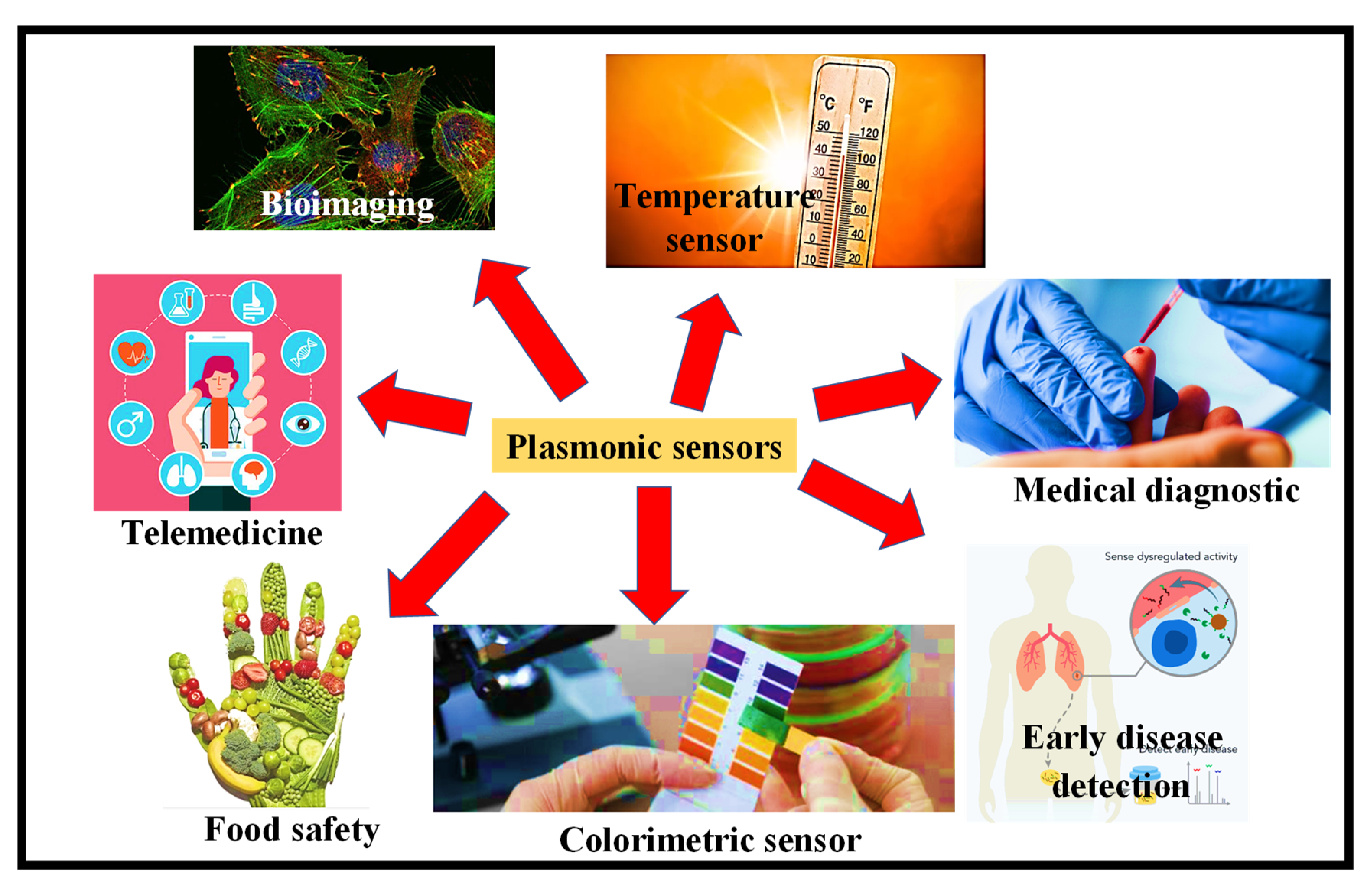
- New Molecular Solutions in Research and Development for Innovative Drugs. Available online: http://www.innomol.eu/Project/Workshops/Bioimaging (accessed on 2 July 2022).
- How Hot Is the Sun? Available online: https://www.space.com/17137-how-hot-is-the-sun.html (accessed on 2 July 2022).
- Available online: https://pl.postermywall.com/index.php/art/template/ea71751b8bb1c640816af0de9fd3d48a/food-safety-day-design-template#.YsAP7HZBzIU (accessed on 2 July 2022).
- The Best Telemedicine Apps to Use During the Coronavirus Pandemic. Available online: https://www.everydayhealth.com/healthy-living/the-best-telemedicine-apps/ (accessed on 2 July 2022).
- The Early Detection Problem. Available online: https://lsi.gatech.edu/early-disease-detection/ (accessed on 2 July 2022).
- Available online: https://www.oakbendmedcenter.org/2020/10/13/what-are-medical-diagnostic-tests-and-how-do-they-work/ (accessed on 2 July 2022).
- Novel Virus-Based Colorimetric Sensor Can Show true Colors of Airborne Threats. Available online: https://phys.org/news/2020-09-virus-based-colorimetric-sensor-true-airborne.html (accessed on 2 July 2022).
- Hamza, M.; Othman, M.; Swillam, M. Plasmonic Biosensors: Review. Biology 2022, 11, 621. [Google Scholar] [CrossRef]
- Saylan, Y.; Akgonullu, S.; Denizli, A. Plasmonic Sensors for monitoring Biological and Chemical threat agents. Biosensors 2020, 10, 142. [Google Scholar] [CrossRef]
- Zhou, N.; Xu, X.; Hammack, A.; Stipe, B.; Gao, K.; Scholz, W.; Gage, E. Plasmonic near-field transducer for heat-assisted magnetic recording. Nanophotonics 2014, 3, 141–155. [Google Scholar] [CrossRef]
- Zhang, J.; Elkabbash, M.; Wei, R.; Singh, S.; Lam, B.; Guo, C. Plasmonic metasurfaces with 42.3% transmission efficiency in the visible. Light Sci. Appl. 2019, 8, 53. [Google Scholar] [CrossRef] [PubMed] [Green Version]
- Available online: https://www.futuremarketinsights.com/reports/surface-plasmon-resonance-spr-systems-market (accessed on 2 July 2022).
- Khonina, S.N.; Kazanskiy, N.L.; Butt, M.A.; Kazmierczak, A.; Piramidowicz, R. Plasmonic sensor based on metal-insulator-metal waveguide square ring cavity filled with functional material for the detection of CO2 gas. Opt. Express 2021, 29, 16584. [Google Scholar] [CrossRef] [PubMed]
- Kazanskiy, N.L.; Khonina, S.N.; Butt, M.A.; Kazmierczak, A.; Piramidowicz, R. A numerical investigation of a plasmonic sensor based on a metal-insulator-metal waveguide for simultaneous detection of biological analytes and ambient temperature. Nanomaterials 2021, 11, 2551. [Google Scholar] [CrossRef] [PubMed]
- Chen, Z.-X.; Wu, Z.-J.; Ming, Y.; Zhang, X.-J.; Lu, Y.-Q. Hybrid plasmonic waveguide in a metal V-groove. AIP Adv. 2014, 4, 017103. [Google Scholar] [CrossRef] [Green Version]
- Banan, B.; Tait, R.; Berini, P. Fabrication of metal strip waveguides for optical and microwave data transmission. J. Vac. Sci. Technol. B 2015, 33, 061208. [Google Scholar] [CrossRef]
- Kumar, S.; Kumar, P.; Ranjan, R. A metal-cap wedge shape hybrid plasmonic waveguide for nano-scale light confinement and long propagation range. Plasmonics 2022, 17, 95–105. [Google Scholar] [CrossRef]
- Dai, D.; He, S. A silicon-based hybrid plasmonic waveguide with a metal cap for a nano-scale light confinement. Opt. Express 2009, 17, 16646–16653. [Google Scholar] [CrossRef]
- Berini, P. Plasmon-polariton waves guided by thin lossy metal films of finite width:bound modes of symmetric structures. Phys. Rev. B 2000, 61, 10484–10503. [Google Scholar] [CrossRef]
- Dionne, J.; Sweatlock, L.; Atwater, H. Planar metal plasmon waveguides: Frequency-dependent dispersion, propagation, localization, and loss beyond the free electron model. Phys. Rev. B 2005, 72, 075405. [Google Scholar] [CrossRef] [Green Version]
- Dionne, J.; Sweatlock, L.; Atwater, H. Plasmon slot waveguides: Towards chip-scale propagation with subwavelength-scale localization. Phys. Rev. B 2006, 73, 035407. [Google Scholar] [CrossRef] [Green Version]
- Zia, R.; Selker, M.; Catrysse, P.; Brongersma, M. Geometries and materials for subwavelength surface plasmon modes. J. Opt. Soc. Am. A 2004, 21, 2442–2446. [Google Scholar] [CrossRef] [PubMed] [Green Version]
- Gordon, R. Light in a subwavelength slit in a metal: Propagation and reflection. Phys. Rev. B 2006, 73, 153405. [Google Scholar] [CrossRef]
- Bozhevolnyi, S.; Volkov, V.; Devaux, E.; Laluet, J.-Y.; Ebbesen, T. Channel plasmon subwavelength waveguide components including interferometers and ring resonators. Nature 2006, 440, 508–511. [Google Scholar] [CrossRef]
- Jafarian, B.; Nozhat, N.; Granpayeh, N. Analysis of a triangular-shaped plasmonic metal-insulator-metal Bragg grating waveguide. J. Opt. Soc. Korea 2011, 15, 118–123. [Google Scholar] [CrossRef] [Green Version]
- Butt, M.A.; Khonina, S.N.; Kazanskiy, N.L. Ultra-short lossless plasmonic power splitter design based on metal-insulator-metal waveguide. Laser Phys. 2019, 30, 016201. [Google Scholar] [CrossRef]
- Butt, M.A.; Khonina, S.N.; Kazanskiy, N.L. Plasmonic refractive index sensor based on M-I-M square ring resonator. In Proceedings of the International Conference on Computing, Electronic and Electrical Engineering (ICE Cube), Quetta, Pakistan, 12–13 November 2018; pp. 1–4. [Google Scholar]
- Butt, M.A.; Khonina, S.N.; Kazanskiy, N.L. Plasmonic refractive index sensor based on metal-insulator-metal waveguides with high sensitivity. J. Mod. Opt. 2019, 66, 1038–1043. [Google Scholar] [CrossRef]
- Butt, M.A.; Khonina, S.N.; Kazanskiy, N.L. A multichannel metallic dual nano-wall square split-ring resonator:design analysis and applications. Laser Phys. Lett. 2019, 16, 126201. [Google Scholar] [CrossRef]
- Butt, M.A.; Khonina, S.N.; Kazanskiy, N.L. Hybrid plasmonic waveguide-assisted metal-insulator-metal ring resonator for refractive index sensing. J. Mod. Opt. 2018, 65, 1135–1140. [Google Scholar] [CrossRef]
- Min, C.; Veronis, G. Absorption switches in metal-dielectric-metal plasmonic waveguides. Opt. Express 2009, 17, 10757–10766. [Google Scholar] [CrossRef]
- Liu, J.; Wang, L.; He, M.; Huang, W.; Wang, D.; Zou, B.; Wen, S. A wide bandgap plasmonic Bragg reflector. Opt. Express 2008, 16, 4888–4894. [Google Scholar] [CrossRef]
- Butt, M.A.; Khonina, S.N.; Kazanskiy, N.L. A plasmonic colour filter and refractive index sensor applications based on metal-insulator-metal square micro-ring cavities. Laser Phys. 2020, 30, 016205. [Google Scholar] [CrossRef]
- Lu, X.; Wan, R.; Zhang, T. Metal-dielectric-metal based narrow band absorber for sensing applications. Opt. Express 2015, 23, 29842–29847. [Google Scholar] [CrossRef] [PubMed]
- McPeak, K.; Jayanti, S.; Kress, S.; Meyer, S.; Lotti, S.; Rossinelli, A.; Norris, D. Plasmonic films can easily be better: Rules and Recipes. ACS Photonics 2015, 2, 326–333. [Google Scholar] [CrossRef] [PubMed]
- Guay, J.; Lesina, A.C.; Cote, G.; Charron, M.; Poitras, D.; Ramunno, L.; Berini, P.; Weck, A. Laser-induced plasmonic colours on metals. Nat. Commun. 2017, 8, 16095. [Google Scholar] [CrossRef] [PubMed]
- Johnson, P.; Christy, R. Optical constants of the Noble Metals. Phys. Rev. 1972, 6, 4370–4379. [Google Scholar] [CrossRef]
- Yakubovsky, D.; Arsenin, A.; Stebunov, Y.; Fedyanin, D.; Volkov, V. Optical constants and structural properties of thin gold films. Opt. Express 2017, 25, 25574–25587. [Google Scholar] [CrossRef] [Green Version]
- Cheng, F.; Yang, X.; Gao, J. Ultrasensitive detection and characterization of molecules with infrared plasmonic metamaterials. Sci. Rep. 2015, 5, 14327. [Google Scholar] [CrossRef] [PubMed] [Green Version]
- Zhong, Y.; Malagari, S.; Hamilton, T.; Wasserman, D. Review of mid-infrared plasmonic materials. J. Nanophotonics 2015, 9, 093791. [Google Scholar] [CrossRef] [Green Version]
- Kunz, J.; Voronine, D.; Lu, W.; Liege, Z.; Lee, H.; Zhang, Z.; Scully, M. Aluminum plasmonic nanoshielding in ultraviolet inactivation of bacteria. Sci. Rep. 2017, 7, 9026. [Google Scholar] [CrossRef]
- Knight, M.; King, N.; Liu, L.; Everitt, H.; Nordlander, P.; Halas, N. Aluminum for plasmonics. ACS Nano 2014, 8, 834–840. [Google Scholar] [CrossRef] [PubMed]
- Dabos, G.; Manolis, A.; Tsiokos, D.; Ketzaki, D.; Chatzianagnostou, E.; Markey, L.; Rusakov, D.; Weeber, J.-C.; Dereux, A.; Giesecke, A.-L.; et al. Aluminum plasmonic waveguides co-integrated with Si3N4 photonics using CMOS processes. Sci. Rep. 2018, 8, 13380. [Google Scholar] [CrossRef] [PubMed] [Green Version]
- Chen, Q.; Cumming, D. High transmission and low color cross-talk plasmonic color filters using triangular-lattice hole arrays in aluminum films. Opt. Express 2010, 18, 14056–14062. [Google Scholar] [CrossRef]
- Dai, P.; Wang, Y.; Zhu, X.; Shi, H.; Chen, Y.; Zhang, S.; Yang, W.; Chen, Z.; Xiao, S.; Duan, H. Transmissive structural color filters using vertically coupled aluminum nanohole/nanodisk array with a triangular-lattice. Nanotechnology 2018, 29, 395202. [Google Scholar] [CrossRef]
- Mivelle, M.; van Zanten, T.; Neumann, L.; van Hulst, N.; Garcia-Parajo, M. Ultrabright bowtie nanoaperture antenna probes studied by single molecule fluorescence. Nano Lett. 2012, 12, 5972–5978. [Google Scholar] [CrossRef]
- White, J.; Veronis, G.; Yu, Z.; Barnard, E.; Chandran, A.; Fan, S.; Brongersma, M. Extraordinary optical absorption through subwavelength slits. Opt. Lett. 2009, 34, 686–688. [Google Scholar] [CrossRef] [PubMed]
- Nguyen, B.; Nguyen, V. Advances in graphene-based optoelectronics, plasmonics and photonics. Adv. Nat. Sci.-Nanosci. Nanotechnol. 2016, 7, 013002. [Google Scholar] [CrossRef]
- Szunertis, S.; Boukherroub, R. Graphene-based biosensors. Interface Focus 2018, 8, 20160132. [Google Scholar] [CrossRef]
- Rodrigo, D.; Limaj, O.; Janner, D.; Etezadi, D.; de Abajo, F.; Pruneri, V.; Altug, H. Mid-infrared plasmonic biosensing with graphene. Science 2015, 349, 165–168. [Google Scholar] [CrossRef] [Green Version]
- Hu, H.; Yang, X.; Zhai, F.; Hu, D.; Liu, R.; Liu, K.; Sun, Z.; Dai, Q. Far-field nanoscale infrared spectroscopy of vibrational fingerprints of molecules with graphene plasmons. Nat. Commun. 2016, 7, 12334. [Google Scholar] [CrossRef] [Green Version]
- Hu, H.; Yang, X.; Guo, X.; Khaliji, K.; Biswas, S.; de Abajo, F.G.; Low, T.; Sun, Z.; Dai, Q. Gas identification with graphene plasmoncs. Nat. Commun. 2019, 10, 1131. [Google Scholar] [CrossRef] [PubMed]
- Losurdo, M.; Yi, C.; Suvorova, A.; Rubanov, S.; Kim, T.; Giangregorio, M.; Jiao, W.; Bergmair, I.; Bruno, G.; Brown, A. Demonstrating the capability of the high-performance plasmonic gallium-graphene couple. ACS Nano 2014, 8, 3031–3041. [Google Scholar] [CrossRef] [PubMed]
- Pau, J.; Garcia-Marin, A.; Hernandez, M.; Lorenzo, E.; Piqueras, J. Optical biosensing platforms based on Ga-graphene plasmonic structures on Cu, quartz and SiO2/Si substrates. Phys. Status Solidi B 2016, 253, 664–670. [Google Scholar] [CrossRef]
- Zeng, S.; Sreekanth, K.V.; Shang, J.; Yu, T.; Chen, C.K.; Yin, F.; Baillargeat, D.; Coquet, P.; Ho, H.P.; Kabashin, A.V.; et al. Graphene-Gold metasurface architectures for ultrasensitive plasmonic biosensing. Adv. Mater. 2015, 27, 6163–6169. [Google Scholar] [CrossRef] [PubMed]
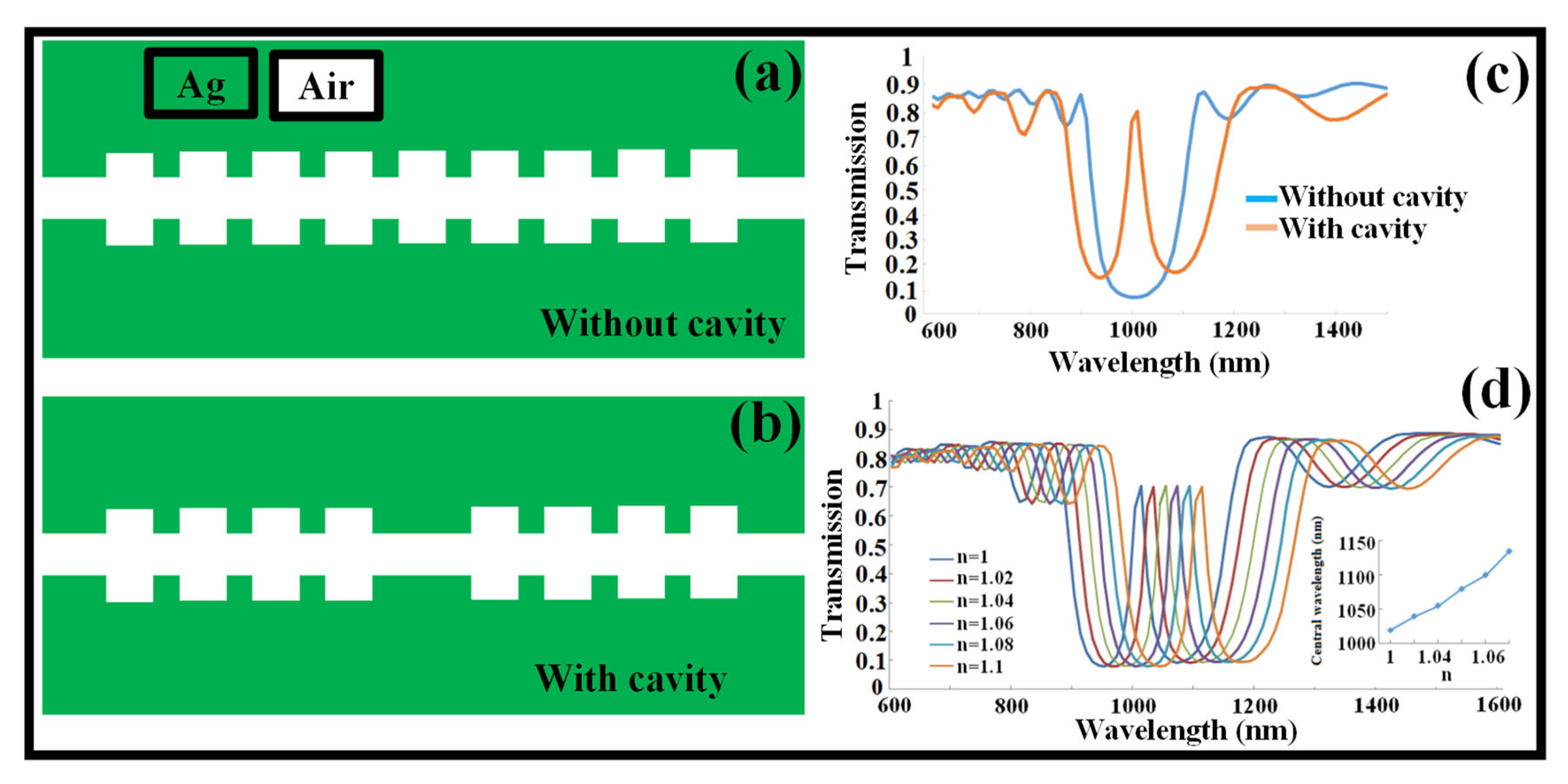
- Boltasseva, A.; Bozhevolnyi, S.; Nikolajsen, T.; Leosson, K. Compact Bragg gratings for long-range surface plasmon polaritons. J. Lightwave Technol. 2006, 24, 912–918. [Google Scholar] [CrossRef]
- Wang, B.; Wang, G. Plasmon Bragg reflectors and nanocavities on flat metallic surfaces. Appl. Phys. Lett. 2005, 87, 013107. [Google Scholar] [CrossRef]
- Hosseini, A.; Massoud, Y. A low-loss metal-insulator-metal plasmonic Bragg reflector. Opt. Express 2006, 14, 11318–11323. [Google Scholar] [CrossRef]
- Hosseini, A.; Massoud, Y. Subwavelength plasmonic Bragg reflector structures for on-chip optoelectronic applications. In Proceedings of the International Symposium on Circuits and Systems, New Orleans, LA, USA, 27–30 May 2007; pp. 2283–2286. [Google Scholar]
- Han, Z.; Forsberg, E.; He, S. Surface plasmon Bragg gratins formed in metal-insulator-metal waveguides. IEEE Photon. Technol. Lett. 2007, 19, 91–93. [Google Scholar] [CrossRef]
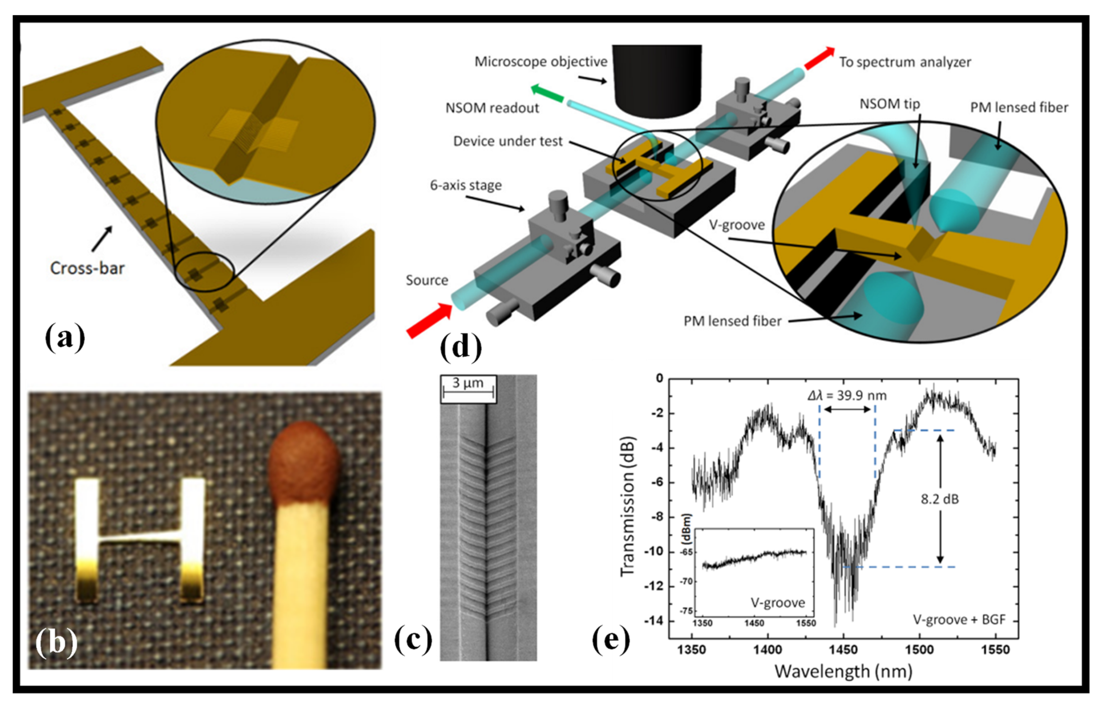
- Smith, C.; Desiatov, B.; Goykmann, I.; Fernandez-Cuesta, I.; Levy, U.; Kristensen, A. Plasmonic V-groove waveguides with Bragg grating filters via nanoimprint lithography. Opt. Express 2012, 20, 5696. [Google Scholar] [CrossRef] [Green Version]
- Lin, D.; Chang, C.; Chen, Y.; Yang, D.; Lin, M.; Yeh, J.; Liu, J.; Kuan, C.; Yeh, C.; Lee, C. Beaming light from a subwavelength metal slit surrounded by dielectric surface gratings. Opt. Express 2006, 14, 3503–3511. [Google Scholar] [CrossRef]
- Dionne, J.; Lezec, H.; Atwater, H. Highly confined photon transport in subwavelength metallic slot waveguides. Nano Lett. 2006, 6, 1928–1932. [Google Scholar] [CrossRef] [PubMed]
- Park, J.; Kim, H.; Lee, B. High order plasmonic Bragg reflection in the metal-insulator-metal waveguide Bragg grating. Express 2008, 16, 413. [Google Scholar] [CrossRef] [PubMed]
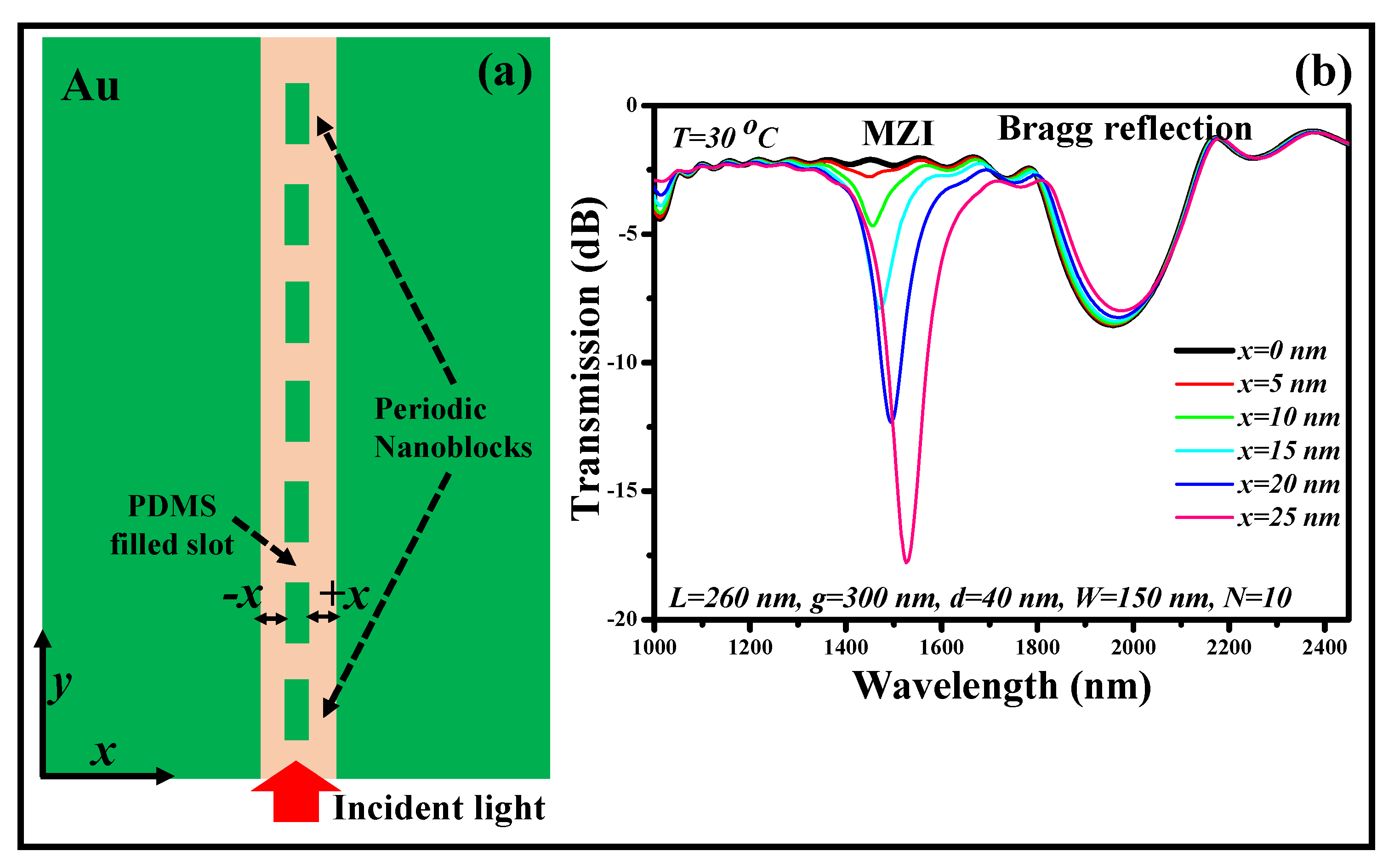
- Qu, S.; Song, C.; Xia, X.; Liang, X.; Tang, B.; Hu, Z.-D.; Wang, J. Detuned plasmonic Bragg grating sensor based on a defect metal-insulator-metal waveguide. Sensors 2016, 16, 784. [Google Scholar] [CrossRef] [PubMed] [Green Version]
- Butt, M.; Khonina, S.; Kazanskiy, N. A compact design of a modified Bragg grating filter based on a metal-insulator-metal waveguide for filtering and temperature sensing applications. Optik 2022, 251, 168466. [Google Scholar] [CrossRef]
- Xu, Y.; Yue, J.; Wang, M.; Sun, X.; Zhang, D. Tunable Narrow-band filter based on long-range surface plasmon polariton waveguide Bragg grating. Photonics 2022, 9, 344. [Google Scholar] [CrossRef]
- Kanso, M.; Cuenot, S.; Louarn, G. Roughness effect on the spr measurements for an optical fibre configuration: Experimental and numerical approaches. J. Opt. A Pure Appl. Opt. 2007, 9, 586. [Google Scholar] [CrossRef]
- Schriver, M.; Regan, W.; Gannett, W.J.; Zaniewski, A.M.; Crommie, M.F.; Zettl, A. Graphene as a long-term metal oxidation barrier: Worse than nothing. ACS Nano 2013, 7, 5763–5768. [Google Scholar] [CrossRef]
- Butt, M.; Tyszkiewicz, C.; Wojtasik, K.; Karasinski, P.; Kazmierczak, A.; Piramidowicz, R. Subwavelength grating waveguide structures proposed on the low-cost silica-titania platform for optical filtering and refractive index sensing applications. Int. J. Mol. Sci. 2022, 23, 6614. [Google Scholar] [CrossRef]
- Butt, M.; Kaźmierczak, A.; Tyszkiewicz, C.; Karasiński, P.; Piramidowicz, R. Mode Sensitivity Exploration of Silica–Titania Waveguide for Refractive Index Sensing Applications. Sensors 2021, 21, 7452. [Google Scholar] [CrossRef]
- Butt, M.; Tyszkiewicz, C.; Karasinski, P.; Zieba, M.; Hlushchenko, D.; Baraniecki, T.; Kazmierczak, A.; Piramidowicz, R.; Guzik, M.; Bachmatiuk, A. Development of a low-cost silica-titania optical platform for integrated photonics applications. Opt. Express 2022, 30, 23678. [Google Scholar] [CrossRef]
- Butt, M.A.; Kazmierczak, A.; Tyszkiewicz, C.; Karasiński, P.; Środa, E.; Olszewski, J.; Pala, P.; Martynkien, T.; Hlushchenko, D.; Baraniecki, T.; et al. HYPHa project: A low-cost alternative for integrated photonics. Photonics Lett. Pol. 2022, 14, 25–27. [Google Scholar]


| Polymer Type | Manufacturer | Optical Losses | Refractive Index |
|---|---|---|---|
| Cyclic olefin copolymer | Topas advanced polymers company | 0.5 dB/cm at 830 nm, 0.7 dB/cm at 1550 nm | 1.53 |
| CyclotoneTM | DOW Chemical | 0.81 dB/cm at 1300 nm | 1.552 @ 633 nm, 1.537 at 1310 nm and 1.535 at 1550 nm |
| EpoCore | Micro resist technology GmbH | 0.2 dB/cm at 850 nm | 1.580 at 850 nm |
| ExguideTM | FOWG series from Chemoptics Inc. (Daejeon, Korea) | <0.1 dB/cm at 850 nm | 1.547 at 830 nm |
| TruemodeTM | Exxelis | 0.04 dB/cm at 850 nm | 1.57 at 633 nm |
| Ultradel 9120D | Amoco Chemicals | 0.34 dB/cm at 850 nm, 0.43 dB/cm at 1300 nm | 1.547 at 850 nm and 1.535 at 1550 nm |
| OE-4140 UV | Dow Corning | 0.04 dB/cm at 850 nm | 1.52 @ 850 nm |
Publisher’s Note: MDPI stays neutral with regard to jurisdictional claims in published maps and institutional affiliations. |
© 2022 by the authors. Licensee MDPI, Basel, Switzerland. This article is an open access article distributed under the terms and conditions of the Creative Commons Attribution (CC BY) license (https://creativecommons.org/licenses/by/4.0/).
Share and Cite
Butt, M.A.; Kazanskiy, N.L.; Khonina, S.N. Advances in Waveguide Bragg Grating Structures, Platforms, and Applications: An Up-to-Date Appraisal. Biosensors 2022, 12, 497. https://doi.org/10.3390/bios12070497
Butt MA, Kazanskiy NL, Khonina SN. Advances in Waveguide Bragg Grating Structures, Platforms, and Applications: An Up-to-Date Appraisal. Biosensors. 2022; 12(7):497. https://doi.org/10.3390/bios12070497
Chicago/Turabian StyleButt, Muhammad A., Nikolay L. Kazanskiy, and Svetlana N. Khonina. 2022. "Advances in Waveguide Bragg Grating Structures, Platforms, and Applications: An Up-to-Date Appraisal" Biosensors 12, no. 7: 497. https://doi.org/10.3390/bios12070497