Article

Thin-Film-Based Multifunctional System for Optical Detection and Thermal Treatment of Biological Samples

by
Nicola Lovecchio
1,*,
Francesca Costantini
1,2,
Augusto Nascetti
3,
Giampiero de Cesare
1 and
Domenico Caputo
1
1
Department of Information Engineering, Electronics and Telecommunications, Sapienza University of Rome, 00184 Rome, Italy
2
CREA-DC Research Centre for Plant Protection and Certification, 00156 Rome, Italy
3
School of Aerospace Engineering, Sapienza University of Rome, 00138 Rome, Italy
*
Author to whom correspondence should be addressed.
Biosensors 2022, 12(11), 969; https://doi.org/10.3390/bios12110969
Submission received: 30 September 2022 / Revised: 24 October 2022 / Accepted: 31 October 2022 / Published: 4 November 2022

Abstract

:
In this work, we present a multifunctional Lab-on-Chip (LoC) platform based on hydrogenated amorphous silicon sensors suitable for a wide range of application in the fields of biochemical and food quality control analysis. The proposed system includes a LoC fabricated on a 5 cm × 5 cm glass substrate and a set of electronic boards for controlling the LoC functionalities. The presented Lab-on-Chip comprises light and temperature sensors, a thin film resistor acting as a heating source, and an optional thin film interferential filter suitable for fluorescence analysis. The developed electronics allows to control the thin film heater, a light source for fluorescence and absorption measurements, and the photosensors to acquire luminescent signals. All these modules are enclosed in a black metal box ensuring the portability of the whole platform. System performances have been evaluated in terms of sensor optical performances and thermal control achievements. For optical sensors, we have found a minimum number of detectable photons of 8 × 10⁴ s−1·cm−2 at room temperature, 1.6 × 10⁶ s−1·cm−2 in presence of fluorescence excitation source, and 2.4 × 10⁶ s−1·cm−2 at 90 °C. From a thermal management point of view, we have obtained heating and cooling rates both equal to 2.2 °C/s, and a temperature sensor sensitivity of about 3 mV/°C even in presence of light. The achieved performances demonstrate the possibility to simultaneously use all integrated sensors and actuators, making promising the presented platform for a wide range of application fields.

1. Introduction

Portability, quick response time, and low reagents consumption are just some of the Lab-on-Chip (LoC) advantages that have led this technology to be among the major research focus of many academic and industrial groups over the last two decades [1,2,3,4,5]. The applications that can be developed by using LoC-based systems cover several research fields, starting from environment monitoring [6,7,8] toward health care and biomedical applications for disease detection and treatment [9,10,11,12,13].
Among these fields, the concept of “true” Lab-on-Chip began to catch on more and more, highlighting increasingly differences between real portable devices and those that can be defined Chip-on-a-Lab due to the bulky external components they need [14,15,16,17]. For this reason, integration has become the key focus of these kinds of systems, and a lot of research works can be found in the literature on how to integrate and miniaturize sensors and actuators [18,19,20,21].
Looking at the integration possibilities, hydrogenated amorphous silicon (a-Si:H) is an appealing material, since it is suitable for developing both active and passive devices on a variety of substrates and on large areas [22,23,24,25]. Thanks to the low thermal budget required by the Plasma Enhanced Chemical Vapor Deposition (PECVD) technique [26,27,28], the a-Si:H can be deposited on silicon, glass, metals, several plastic substrates, and so forth, allowing therefore the integration and miniaturization levels that a “true” Lab-on-Chip requires [29,30].
The possible applications of amorphous silicon-based devices range from multilayer color detectors [31] to active matrices for liquid-crystal displays [32], from thin-film photovoltaic cells [33] to one-, two-, or three-dimensional optical position detectors [34], and its wide use is due both to the intrinsic properties of the material and the mature fabrication technologies. Recently, a-Si:H has been used also for developing light and temperature sensors in Lab-on-Chip applications [35,36,37,38,39], demonstrating the great potential this material has to offer.
In this work, we present a portable LoC-based multifunctional system that, by exploiting the abovementioned properties of the amorphous silicon, allows its use in all applications where the optical detection in the visible range can be used for the detection and quantification of the target analyte. In particular, in Section 2, we report on the structure and operation of the system, describing in detail the design and fabrication process of each module. In Section 3, we evaluate the platform’s intrinsic performances in the framework of feasible applications of the system, without considering the effect of specific samples under analysis. Finally, in Section 4, we summarize the obtained results.

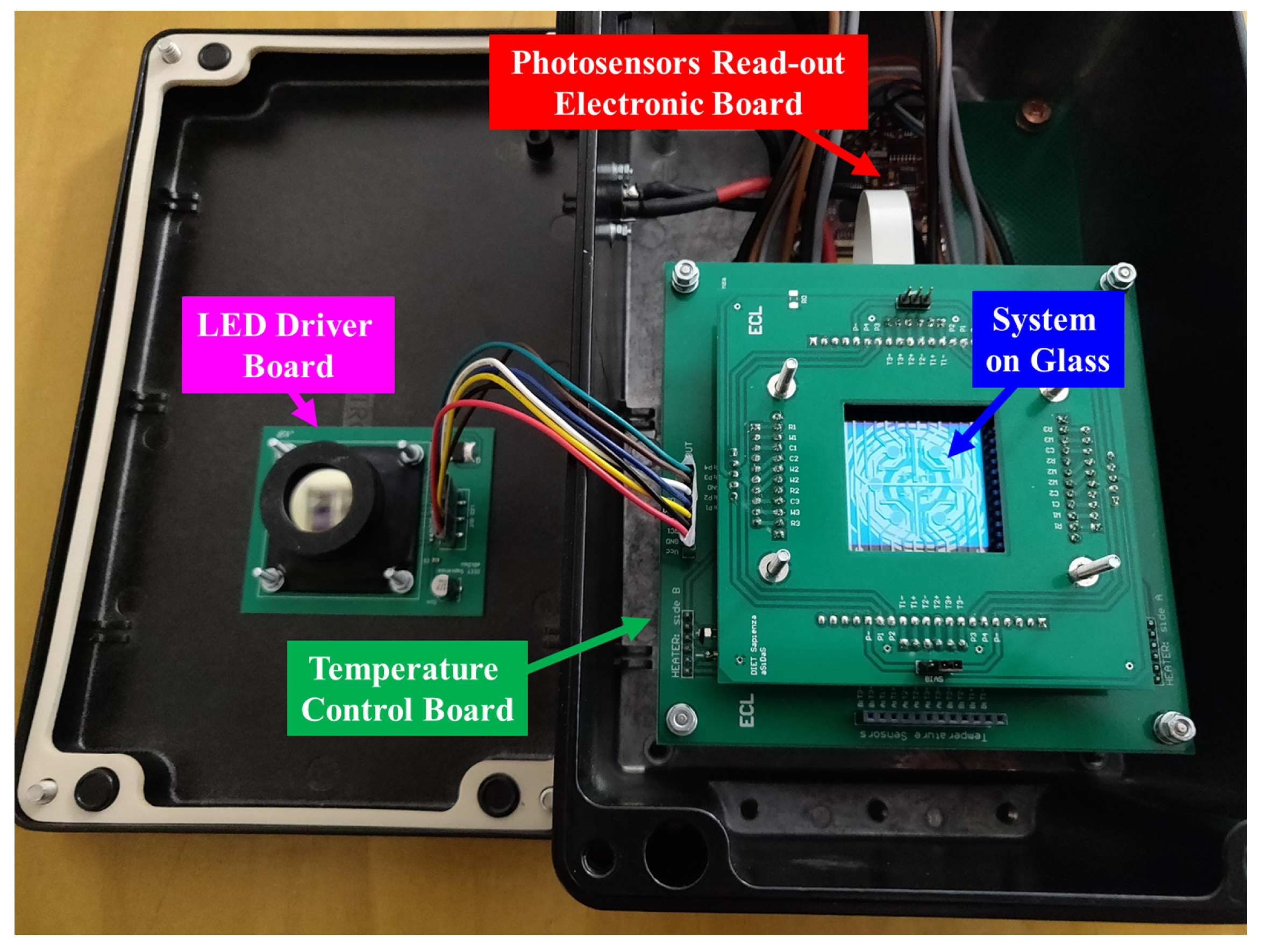
2. System Structure and Operation

A schematic block diagram showing all the modules of the system is depicted in Figure 1.
The core of the system is the Lab-on-Chip, also called System-on-Glass (SoG), which is a 5 cm × 5 cm glass substrate hosting a thin film heater, a-Si:H light and temperature sensors, and an optional thin film interferential filter suitable for all the applications requiring the fluorescence detection. Thanks to a low-noise charge integrator-based read-out electronics (red block in Figure 1), the optical detection in the visible spectrum range can be performed, including fluorescence-based applications that need an excitation source (violet block). Simultaneously, it is possible to apply thermal treatments on the target analyte thanks to the temperature control board (green block), which infers the temperature by the a-Si:H temperature sensors and drives the thin-film heater to reach the desired temperature. Finally, a custom graphical user interface (yellow block), developed in Visual C++, allows the users to control the complete system.
All these modules, including the LoC with an ad hoc connector for electrical contacting sensors and heater, are enclosed in a black metallic box whose dimensions are 26 cm × 16 cm × 12 cm, as shown in Figure 2. The total weight of the metallic box is below 2 kg.
A detailed description of the SoG and an explanation on how each module works are reported in the following Subsections.

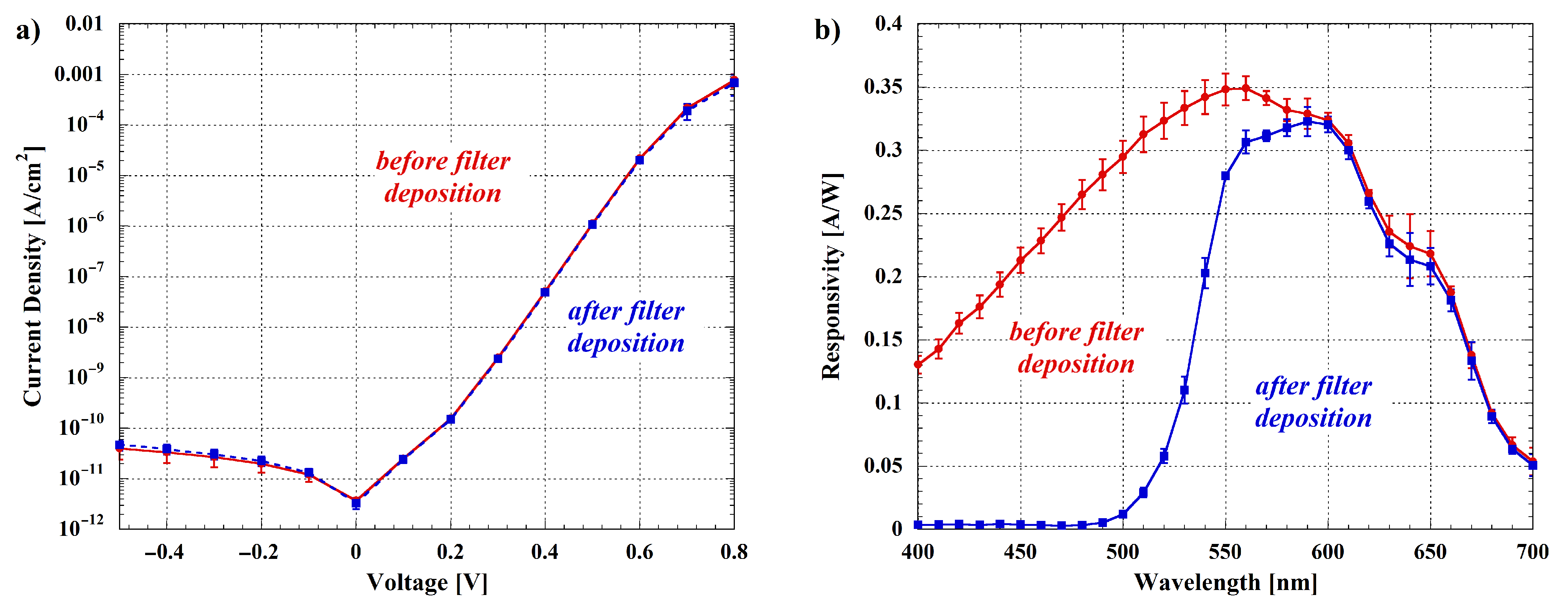
2.1. System-on-Glass

Figure 3 shows the schematic cross-section of the LoC.
The LoC is fabricated on a BOROFLOAT® 33 glass substrate from Schott, United Kingdom, which is a high-quality borosilicate glass with good physical properties including high transmission in the visible and infrared light ranges, operating temperature up to 450 °C, resistance against strong acids, bases, and organic substances, low coefficient of thermal expansion, and so forth. All sensors and actuators mentioned above have been integrated on both sides of the substrate, as shown in Figure 4, where a picture of the fabricated System-on-Glass, together with a schematic representation of the heater and the sensors geometries, is reported.
The heater, fabricated on the bottom side of the proposed SoG, is a double concentric spiral-shaped resistor, designed and optimized in terms of pitch and line width by using COMSOL Multiphysics® in order to achieve a uniform temperature distribution, with a temperature variation below 1.5 °C over an about 5 cm2 area and up to 100 °C. A detailed description of this heater in terms of static and dynamic response to heating can be found in [40]. On the top side of the SoG, eight photosensors (four round-shaped with a 3 mm diameter, corresponding to a 7 mm2 area, and four with semirounded shape with a 3.5 mm2 area) have been positioned on a radial distribution obtaining the same dynamic evolution of the temperature during heating. Finally, six square temperature sensors of 1 mm2 area have been integrated on the same side: four of them are positioned on the same photosensors radial distribution, while the other ones are placed on the central area.
The presented chip is fabricated according to the technological steps reported below in sequential order:
1.
ultrasonic cleaning of the glass substrate;
2.
sensors side:
(a)
deposition of a sacrificial protection layer of a 400 nm-thick titanium-tungsten (Ti-W) alloy in a three-targets Material Research Corporation RF magnetron sputtering system;
3.
heater side:
(a)
deposition of a 45 nm-thick indium-tin oxide (ITO) layer acting as a ground plane through the same RF magnetron sputtering system;
(b)
deposition of the insulation layer of a 5 µm-thick SU-8 3005 film by spin coating and its patterning to expose the contacts to connect the ground plane;
(c)
deposition, by vacuum evaporation, of a chromium (Cr)/aluminum (Al)/ chromium (30/600/70 nm) stacked layer by means of a Balzers 510 evaporation system and its patterning to define the thin film heater by means of standard optical lithography and wet etching processes;
(d)
definition of a passivation layer through the spin coating of a 5 µm-thick SU-8 3005;
4.
sensors side:
(a)
removal of the Ti-W sacrificial protection layer;
(b)
deposition of a Cr/Al/Cr (30/150/30 nm) stacked layer and its patterning to define the sensors bottom contacts;
(c)
deposition of the a-Si:H structure by means of a Glasstech Solar Incorporation three-chamber ultra-high vacuum PECVD system;
(d)
evaporation of a 50 nm-thick Cr layer, acting as the sensors top contact;
(e)
Cr wet etching and a-Si:H dry etching in Ionvac Reactive Ion Etching (RIE) system for the mesa patterning of the diodes;
(f)
deposition of the insulation layer by spin coating of a 5 µm-thick SU-8 3005 film and its patterning for the opening of the via holes;
(g)
sensors side: deposition of a 250 nm-thick Ti-W alloy and its patterning for the definition of the top contact and the connection to the pads, located on the glass edge;
(h)
definition of a passivation layer through the spin coating of a 5 µm-thick SU-8 3005 film;
(i)
optional deposition of a multilayer stacked structure of titanium oxide (TiO2)/ silicon oxide (SiO2) dielectric layers acting as thin film interferential filter.
Thanks to the design optimization of the system, all the integrated sensors and actuators can operate simultaneously without loosing in performances. In particular, temperature sensors and photodiodes are fabricated in the same deposition run; for this reason, the thicknesses of the p-i-n junction layers have been optimized to have both high sensitivity to light and good linearity and stability when the diodes are used as temperature sensors [25]. Furthermore, as it can be noted in the cross-section of Figure 3, only the top contact differs for these kind of sensors. In particular, for the photosensors, it consists in a Cr/Al/Cr metal grid realized over a thin transparent layer of chromium silicide, which is autonomously formed when the chromium is deposited on the n-doped amorphous silicon [41]. This configuration allows the light radiation to reach the intrinsic layer, where the electron-hole pair can be photogenerated. On the other hand, for the temperature sensors, the top contact is a uniform metal layer able to shield the light radiation, which must not affect the temperature measurements. In addition to the different configuration of the top contact, also a transparent ground plane has been integrated for uncoupling the heater leakage currents from the sensors, leaving intact their sensitivity and, therefore, the system limit of detection also when heater and sensors are used at the same time.
For all the applications requiring the fluorescence detection, a thin film interferential filter has also been integrated [28]. The filter allows to transmits only the emission spectrum of the used fluorescence molecules, rejecting, at the same time, the excitation wavelengths. This reduces the photosensor background signal and avoids the read-out electronics saturation.

2.2. SoG Connection System

In order to ensure a proper connection between the SoG and the electronics needed to control each module, a custom-made electrical connector based on printed circuit board (PCB) has been developed. A schematic 3D view of the proposed solution is depicted in Figure 5.
The developed connector is composed by two parts, a top and a bottom PCBs. The bottom one integrates two 20-pad connectors for the heater contacts and it is used also to sustain the SoG. On the other hand, the top PCB includes another two 20-pad connectors for the SoG sensors contacts and two supplementary 12-pad connectors suitable to drive optional electrodes. These ones have to be integrated on a 3 cm × 5 cm top substrate, positioned on the top of the LoC as shown in Figure 5. This configuration allows to integrate other sensors and/or actuators to the platform, making feasible the driving, for example, of sensors to monitor conductibility [42,43] or pH [44], electrodes for digital microfluidic [45,46] or electrochemical analysis [47].
The 12- and 20-pad connectors mounted on the PCBs have been obtained by cutting transversely the 5-5530843-4 Edge Card Connector (from TE Connectivity Amp) in order to expose the metallic pads. Moreover, since the substrates can have different heights, some wedges (brown blocks in the figure) are placed under the12-pad connectors in order to correctly contact all of the modules. This kind of connection system ensures both high mechanical stability and strong electrical connection, allowing to reduce contact resistances without damaging the metal thin-film pads of the SoG.
A picture of the realized custom-made connector is reported in Figure 6.

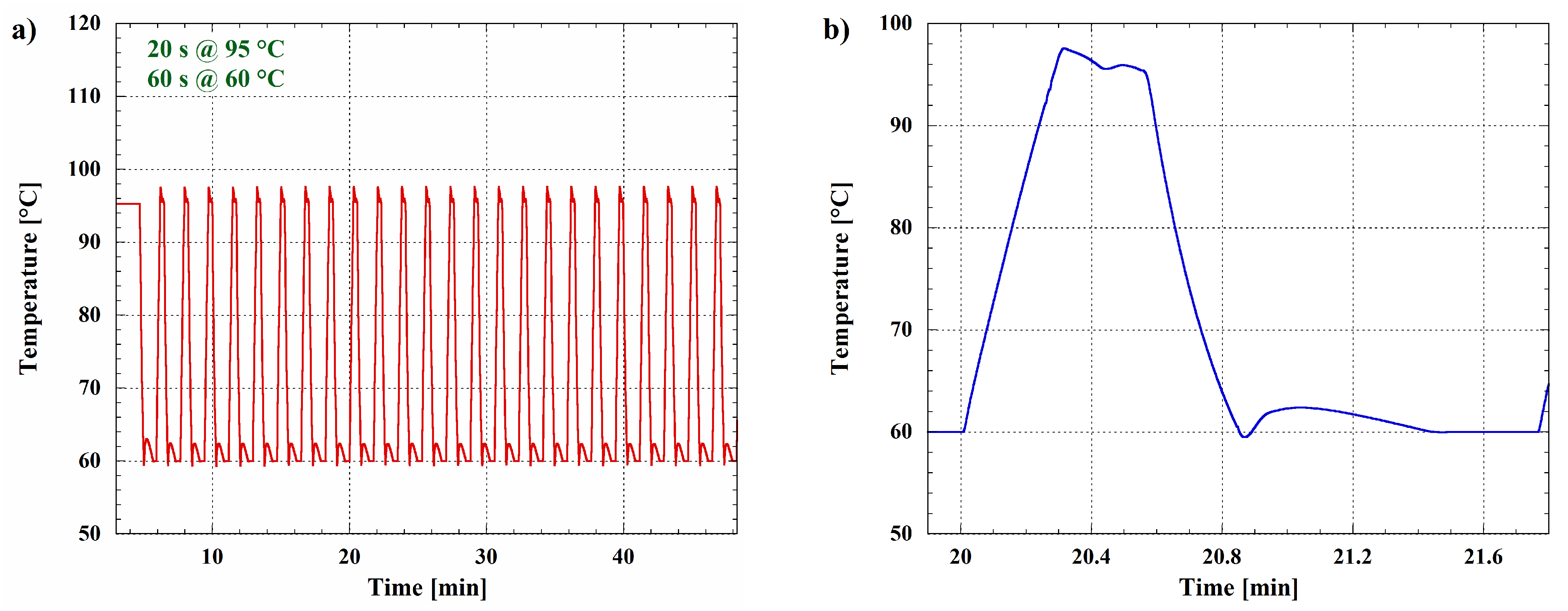
2.3. Thermal Treatment Module

This section describes the temperature control system, including the electronic circuit boards (green block of Figure 1) and the developed proportional–integral–derivative (PID) algorithm [48] to stabilize the temperature. The electronic boards, in turn, include:
  • a power circuit that drives the heater with the current required to achieve the desired temperature;
  • a power circuit that drives a fan used to enhance the cooling of the LoC if it is required by the specific application;
  • an electronic circuit that biases the temperature sensor at a constant current and measures the voltage across the diode junction.
A current generator driven by a digital to analog converter has been used in order to pilot the thin film resistor [49]. Moreover, a fan is placed under the SoG to quickly cool the LoC when the specific application requires thermal cycles or rapid decrease in temperature. The same circuit typology of the heater driver has been used to drive the fan. Both these power circuits have been integrated on the same printed circuit board (PCB), while the circuit that biases the temperature sensors is realized on another PCB (Figure 7). In this way, the electronics employed for the temperature acquisition is uncoupled from the electronic board that hosts the fan and the power circuits, allowing to strongly reduce interferences and, therefore, the noise associated to the temperature detection.
The circuit that infers the heater temperature through the a-Si:H junction (described in [49]) drives a diode with a constant current in forward condition and, at the same time, measures the voltage across the diode. The temperature monitoring is possible since the voltage across the diode used as temperature sensor varies linearly with the temperature when it is biased with a constant current. A detailed characterization of our temperature sensors in terms of sensitivity and stability as a function of the operating point is reported in [25]. Thanks to the electronics optimized design, the minimum detectable voltage signal is about 10 µV that, considering a sensor sensitivity of about −3 mV/°C, corresponds to a temperature value lower than 4 × 10⁻³ °C.
A Graphical User Interface (GUI) controls all of the functionalities of the electronic boards. In particular, a software PID auto-tuned algorithm is used to reach a user-specified setpoint temperature starting from the temperature inferred by the diode. The schematic diagram of the developed algorithm is shown in Figure 8.
The block “Ki Generator”, which is a real-time PID-parameters estimator implemented as a fuzzy-logic controller [50,51], is used to provide for each cycle the proportional (KP), integral (KI), and derivative (KD) gains to the block “PID”. This block, according to the calculated error and the abovementioned parameters, evaluates a value that is proportional to the power dissipated by the heater.
Since the heater current must be a positive value, a limiter block (gray box in Figure 8) has been introduced to ensure that the PID output is not negative and, moreover, does not exceed the maximum current that can be provided to the heater.
In an ideal thermal system, the temperature reached by the Joule effect is proportional to the dissipated power, which is, in turn, proportional to the square of the current. To linearize the algorithm response, a square root block (light blue box in the figure) has been introduced.
Finally, the block called “Process” represents, in this case, the SoG. The input variable v ( t i ) is the current which flows into the heater, while the variable O u t p u t is the voltage across the a-Si:H temperature sensor, and hence the temperature reached by the SoG.
A detailed description of the developed auto-tuned PID algorithm can be found in [52].

2.4. Optical Detection Module

The proposed platform exploits optical detection methods, performed by integrated thin film amorphous silicon-based devices, as a sensitive approach for stimulated fluorescence detection, optical absorption measurements, and chemiluminescence or thermochemiluminescence detection. The optical module includes two electronic boards: one (red block in Figure 1) used for the photocurrent acquisition by the light sensors and another one (violet block in Figure 1) used for controlling a light-emitting diode (LED), which is suitable as the excitation source for both absorption measurements and fluorescence detection.
The first PCB is an eight-channel photocurrent readout electronics that combines selection of the current range (from femtoamps to hundreds of nanoamps), good noise performances, and on-board sensor-bias voltage supply [53]. The read-out electronics includes a dual-switched integrator and performs a continuous signal integration with zero dead-time. Thanks to the careful design, the performances of this system have been optimized to work with amorphous silicon photosensors, obtaining a noise level of about 10 fA [53]. Considering that the area of the abovementioned photosensors is 7 mm2 and their responsivity is about 350 mA/W [54], the minimum detectable signal of this system is of the order of few pW/cm2.
The electronic boards driving the excitation light source include a current generator that controls the LED and a MOSFET-based analog switch, connected in parallel to the LED, to quickly switch-off the excitation source allowing fast blinking operations. On the top of the light source is placed a black 3D-printed holder (visible on the left of Figure 2), in order to lock a collimator and a band-pass filter for directing and shrinking the LED wavelength spectrum, respectively. The board is placed on the box cover and is aligned to the SoG in order to enlighten all the active area, i.e., the 3 cm-diameter round area including all sensors of the LoC. When the box is closed, the distance between the band-pass filter and the SoG is 3 cm.

2.5. Microfluidics

In order to exploit the features that the proposed system can offer, an appropriate microfluidic network, which has to be optically and thermally coupled with the SoG [37,38], should be realized. The distribution of the photosensors on the LoC allows different microfluidic geometries, suitable for both stop-flow or in-flow measurements. Some of the possible shapes of microfluidic wells and channels that can be used with the presented system are shown in Figure 9.
The microfluidic chip can be developed by using different materials, including glass [35], Cyclic Olefin Copolymers (COC) [38], or Polydimethylsiloxane (PDMS) [4]. A picture of the system coupled with a simple black-PDMS six-wells microfluidic chip (Figure 9a) sticked on a 3 cm × 3 cm 200 µm-thick glass substrate is shown in Figure 10, where a 3D-printed holder has been positioned on the top of the SoG to guarantee optical and thermal coupling between the LoC and the microfluidics.

3. Evaluation of System Performances

In this Section, an evaluation of the system performances as a function of the possible applications will be presented. The analysis will range from the detection of a simple chemiluminescent biochemical reaction up to the possibility to perform a real-time three-temperatures polymerase chain reaction (PCR), as reported in the next subsections.
It is worth noting that this evaluation is carried out just in terms of a-Si:H sensors and thin film heater performances independently on the biological sample to be detected and the specific diagnostic, agro-food or clinical application. Therefore, all the achieved results do not consider the effects of the real samples, such as the matrix effect for a food quality control, the luminescent efficiency of the fluorophores in a fluorescence-based detection, and so forth. The specific performances will depend on the considered application and are out of the aim of this work. Hence, the presented evaluations characterize the intrinsic performances of the system, as given by the system-on-glass and the control and read-out electronics.
Moreover, all the below reported measurements refer to a stable behavior of the sensors. Indeed, the optoelectronic characterizations performed on “as grown” temperature and light amorphous silicon sensors show that each sensor modifies its characteristics for repeated measurements and thermal cycles. However, these changes decrease with increasing use and, for this reason, all the reported measurements have been carried out after a few days during which the optoelectronic platform is stressed with continuous thermal cycles. After this treatment, the sensors result stable, since the differences between repeated measurements of the same sensor is less than 1% without showing a monotonic trend.

3.1. Room-Temperature Luminescence Detection

Several LoC-based applications, as can be found in literature, do not need to treat the analyte [55,56,57] but simply perform the detection by using electrochemical [58,59,60], mechanical [61], or optical methods [21,62,63,64]. Among these, the optical detection has been the most widely used technique for quantitative analysis due to its robustness and sensitivity [2].
Chemiluminescence (CL) is a widely employed optical method for analyte detection, where the target binding induces a direct or an enzyme-labeled photochemical emission. This technique is particularly attracting because it avoids the presence of an excitation source, minimizing therefore the background signal noise. For LoC systems, the benefits are even greater since the absence of the excitation source and filters improves the system portability [65]. However, highly sensitive detectors are typically demanded. For this reason, hydrogenated amorphous silicon photosensors are appealing for chemiluminescence detection in the visible wavelength range, since low dark current and good responsivity can be obtained, as shown in Figure 11a and in Figure 11b (red curves), respectively.
By biasing the photosensors with a small reverse voltage (below 100 mV), the related dark current density results to be less than 10 pA/cm2 with an associated shot current noise around 6 fA/(cm2√Hz). Considering that the noise of the read-out electronics is around 10 fA [53] and a limit of detection equal to 3 times the system noise, the minimum detectable photocurrent Iph,min is close to 50 fA/cm2. On the other hand, taking into account that the photon number nph can be derived from the following equation:
n p h = I p h · λ q · R · 1240
where λ is the wavelength, q is the electron charge, and R is the responsivity, the minimum number of detectable photons in a chemiluminescent signal (nph,min) is estimated to be 8 × 10⁴ photons/(s cm2). Up to our knowledge, this value greatly improves the detection limit found in literature [66]. Thanks to the obtained performances, the system allows low limit of detections, as recently demonstrated for several applications [67,68,69].
Even if the CL technique is preferable respect to others photoemission mechanisms due to the intrinsic compactness that derives from this method, the fluorescence detection results to be the widely used method for the analyte detection and quantification in lab-scale applications [70]. Fluorescence is a luminescence mechanism caused by the excitation of fluorescent molecules, through the absorption of the energy coming from an incident radiation. The fluorescent agent re-emits almost immediately (within about 10−8 s), usually at higher wavelengths than the exciting ones. Since the re-emission occurs so quickly, the fluorescence ceases as soon as the exciting source is removed, making the detection of the analyte possible only in presence of the excitation light.
Despite several possibilities for integrating compact fluorescence sensors on LoC systems have been developed [71], the employment of bulk optical components, like lenses or optical fibers, are still used for the coupling of the detector and the fluorescence source [72]. This external optical coupling strongly reduces the portability of the developed systems. The presented platform overcomes these issues, making possible the fluorescence-based detection thanks to the integrated thin film interferential filter, which rejects the excitation source without increasing the distance between the fluorescence site and the photosensors. However, in order to ensure a proper transmittivity range of the interferential filter, the selected fluorescent molecule should have a high Stoke shift, which is the distance between the absorption and the re-emission wavelengths. In this way, it is possible to reject the excitation light by an accurate design of the filter band, and have at the same time the maximum transmittance at the molecule re-emission wavelength. Ruthenium-based fluorophores are very appealing to this aim, since the absorption of these complexes is in the range between ultraviolet (UV) and blue light, while the re-emission spectra are usually positioned beyond 500 nm [73,74]. In particular, the interferential filter integrated on the presented SoG has been dimensioned, as reported in [28], to work with the [Ru(phen)2(dppz)]2+ (phen = 1,10-phenanthroline, dppz = dipyrido[3,2-a:2 ,3 -c]phenazine), a fluorescent dye that shows an absorption peak around 450 nm, and an emission peak located between 610 and 630 nm. Experimental results related to the filter operation are shown in Figure 11b, where the blue curve represents the responsivity of the photosensors after the filter deposition. As expected, the responsivity around 450 nm is below 10−3 A/W, confirming the ability of the interferential filter to reject the excitation light source without degradating the photosensors performances, as also demonstrated by the blue curve of Figure 11a.
To evaluate the system performances in detecting fluorescent signal, we need to take into account not only the noise associated to the sensor dark current and to the read-out electronics but also the noise associated with the background signal due to the excitation light. In order to find this value, we have made several experiments varying the ruthenium complex concentration in the microfluidic holes and the power intensity of the excitation source. We have found that the best compromise for maximizing the signal-to-noise ratio is achieved when the ruthenium complex concentration ranges between 1 and 5 µM while the driving current of the LED radiation source ranges between 0.3 and 0.5 mA. In these conditions, the minimum photocurrent is around 3 nA/cm2, which corresponds to a background radiation shot noise of 40 fA/(cm2√Hz). Once again, considering a limit of detection equal to 3 times the system noise, the minimum detectable photocurrent is close to 150 fA/cm2. Following the Equation (1), we can estimate that nph,min at 610 nm is around 1.6 × 10⁶ photons/(s cm2).
Recently, authors have demonstrated the suitability of the proposed fluorescence detection system in a quality food control application [67]. In particular, the possibility to detect and quantify the concentration of the Ochratoxin A in beer and wheat was demonstrated, obtaining a limit of detection and a limit of quantification of 1.3 ng/mL and 3.9 ng/mL, respectively.
Electrochemiluminescence (ECL) is another photoemission mechanism that can be exploited for the detection and quantification of the target analyte in LoC-based systems [75,76,77]. It is usually observed during the application of a potential (several volts) to the electrodes of an electrochemical cell that contains a solution of luminescent species (polycyclic aromatic hydrocarbons, metal complexes, Quantum Dots or Nanoparticles) in an aprotic organic solvent [78]. To exploit this technique, another substrate integrating transparent electrochemical cell electrodes and microfluidic chambers have to be coupled with the SoG [79,80,81]. Thanks to the developed custom-made connector described in Section 2.2, the ECL technique can also be considered as a future application that could be implemented with the presented system.

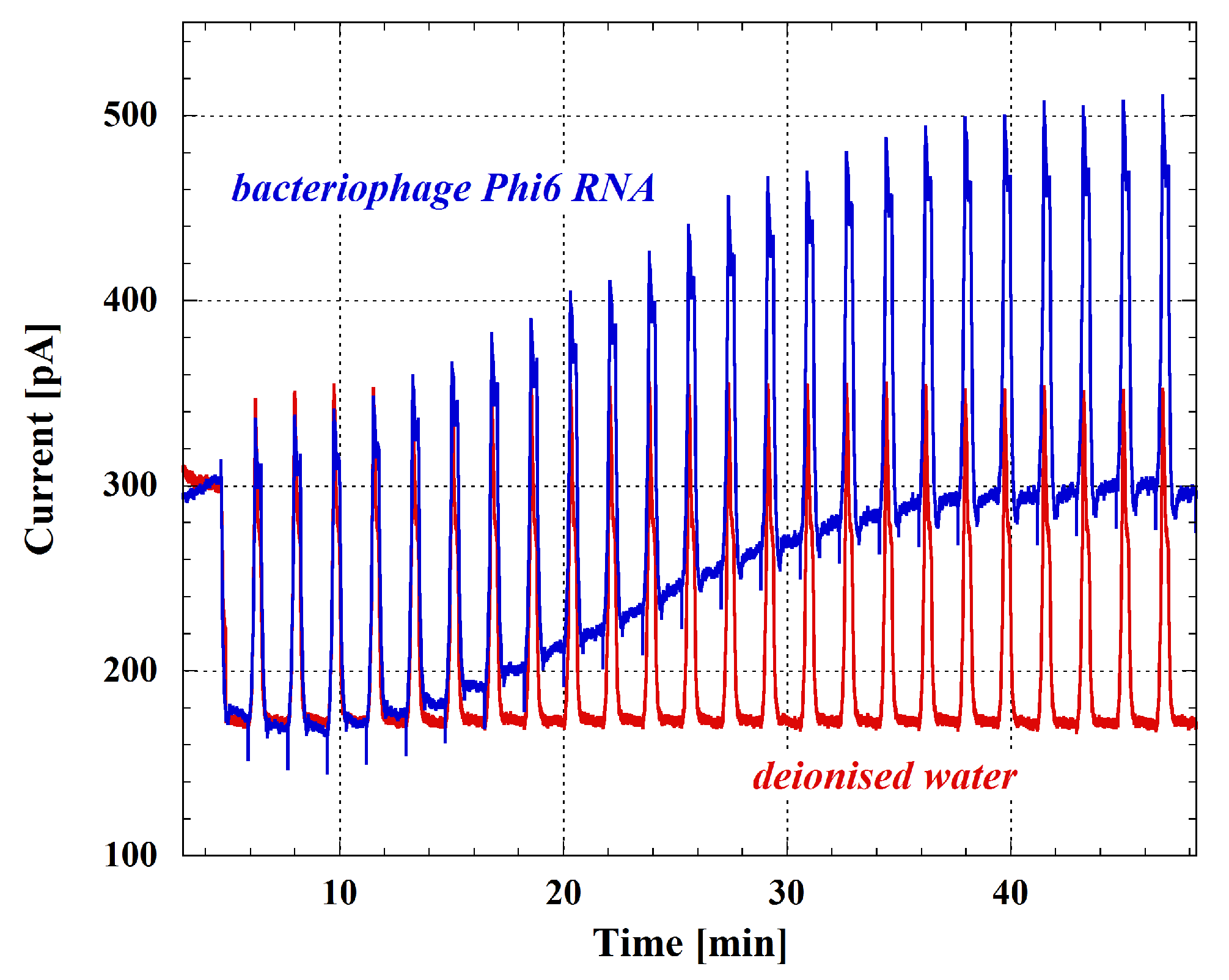
3.2. Luminescence Detection under Thermal Treatment of the Sample

In this Subsection, we will evaluate the system performances when a thermal treatment of the biological sample is considered. As a first example, we consider the thermochemiluminescence (TCL) process. In this case, the emission of light from the molecule is caused by a chemical reaction induced by heating [82]. In order to perform TCL detection by using the presented system, the simultaneous operation of temperature sensors and photosensors have to be guaranteed.
As explained in the Section 2, the different top contact of the two sensors allows to measure the temperature of the LoC even in presence of light, as demonstrated in Figure 12a.
In particular, the figure shows the voltage–temperature (VT) characteristic of the fabricated diodes measured with a 50 nA bias current (corresponding to a current density of 5 µA/cm2), either in dark condition and in presence of a light intensity of about 1.5 mW/cm2, while the inset reports the comparison between the current density–voltage characteristics measured at 30 °C. By looking at the JV curves, it is clear that the presence of light generates a photocurrent that is visible in the reverse voltage bias condition, but which is negligible respect to the bias current, as demonstrated by the agreement of the VT characteristics measured in the two considered conditions.
On the other hand, in order to verify the possibility to use the photosensors during heating, in Figure 12b are reported the JV characteristics measured at different temperatures. As expected, the dark reverse current of the sensors increases exponentially with the temperature, with a consequent raise of the noise related to the light intensity measurement. This exponential law is well known for crystalline silicon diodes as reported in [83], and it applies to a-Si:H diodes too. Even if this matter can represent a limitation for the system usability, it is worth noting that the dark current for reverse voltages near 0 V shows a slow increase, making it feasible to measure the light intensity without major performance losses. Indeed, the dark current measured at 90 °C (a typical value for inducing a thermochemiluminescent process) does not exceed 10 nA/cm2 at reverse voltage below 100 mV. This brings a dark current noise equal to 80 fA/(cm2√Hz). Following the previous calculations and taking into account that the chemiluminescent spectrum is between 400 and 450 nm, this value leads to an estimation of 270 fA/cm2 and 2.4 × 10⁶ photons/(s cm2) for the minimum detectable photocurrent and the minimum detectable number of incident photons, respectively. Obviously, the light intensity measurements must be done only when the temperature is stabilized, since during the temperature variations, it is impossible to uncouple the variation of sensor current due to the light from the variation attributable to the temperature.
Another process where it is crucial the luminescent detection and the thermal treatment of the sample is the real-time DNA/RNA amplification process [84,85,86]. Nucleic acid amplification is a fundamental process in molecular biology, since DNA/RNA copies can be used in a large number of medical and forensic applications. It can likewise be used in the identification and detection of infectious diseases [87,88] and for a wide variety of research purposes in the field of molecular genetics, including genetic engineering [89], characterization of species [90], gene therapy [91], and so forth.
Nucleic acid amplification techniques can be subdivided in two main categories, which are polymerase chain reaction-based and isothermal methods [92]. Temperature changes are the main difference between these techniques: in PCR-based ones, a thermal cycler changes the reaction temperatures repeatedly to affect the actions of the temperature-dependent reagents needed for the amplification process [93]; on the other hand, an isothermal amplification reaction occurs at a single temperature [94].
Currently, PCR and derivative technologies are the gold-standard nucleic acid amplification techniques for sensing applications, as they typically have superior sensitivity and specificity [95]. PCR products can theoretically double once during every thermal cycling event; this can provide a more controlled reaction with better specificity but also limits the reaction speed and product yield. PCR also requires precise temperature control and rapid temperature cycling to denature DNA and subsequently anneal and extend short oligonucleotide primers [96]. As this temperature cycling requires additional equipment and time, isothermal nucleic acid amplification technologies fulfill the need for fast and inexpensive molecular detection methods. For these reasons, the isothermal amplification implementation in point-of-care diagnostic devices is greatly simplified, allowing low sample consumption, multiplex DNA analysis, integration, and portable devices realization [97]. Types of isothermal amplification methods include strand-displacement amplification (SDA), rolling-circle amplification (RCA), whole-genome amplification (WGA), loop-mediated isothermal amplification (LAMP), helicase-dependent amplification (HDA), and multiple displacement amplification (MDA), among others.
The detection phase of the target DNA or RNA sample can be done after the amplification step or in real time, depending on the equipment that the chosen platform provides. In our case, the possibility to exploit simultaneously temperature control and optical monitoring allows to perform real time detection by several ways, as demonstrated in [38,98]. In particular, authors have been demonstrated in [98] that, by using a SoG having different geometries for the heater, photosensors and temperature sensors of the LoC presented in this work, it is possible to implement the LAMP technique. In particular, this technique has been optimized to specifically amplify parvovirus B19 DNA and has been coupled with Bioluminescent Assay in Real Time (BART) technology, in order to provide the real-time detection of target DNA. Furthermore, real-time monitoring of MDA has been also performed [38] by exploiting the fluorescence-based method to detect the calf thymus DNA.
Depending on the typical application, isothermal amplification methods can have lower sensitivity and/or specificity when compared to PCR. For this reason, the performances of the presented platform have been evaluated to demonstrate the effectiveness also in conducting thermal cycles, in order to implement standard and real-time PCR amplification. Figure 13a shows the temperature evolution during a standard two-temperatures PCR reaction [99], considering 95 °C for the denaturation step and 60 °C for the annealing and the DNA extension.
Figure 13b is a magnification related to a single cycle, where it is possible to appreciate the obtained heating and cooling rates, which are both equal to ∼2.2 °C/s.
In order to perform real-time monitoring of the nucleic acid amplification, the system has been tested also in presence of the excitation light source for evaluating the acquired photocurrents. In particular, a first step of the experiment was conducted by filling the six wells of the microfluidic chip shown in Figure 10 with deionized water covered by mineral oil to avoid the fluid evaporation. Results are reported as red curve in Figure 14, where it is possible to observe, as expected, the flat behavior of the photocurrent corresponding to the annealing steps. In this case, the current mean value is due to both the value of the sensors dark current at 60 °C and the background light derived from the switched-on excitation LED.
As a second step of the experiment, the deionized water has been replaced by a PCR reaction mixture containing 6 µL of GoTaq PCR master mix (Promega), 1.25 µL of 10 µM forward and reversed primers, 0.3 µL of ruthenium complex 0.1 mM, 0.2 µL of reverse transcriptase (Promega), 2 µL of nuclease free water (Promega), and 1 µL of RNA extracted from bacteriophage Phi6 [100]. This experiment was performed in order to evaluate the system capabilities to monitor the nucleic acid amplification exploiting the fluorescence detection technique. The blue curve of Figure 14 shows the obtained result and, in particular, it is possible to see the increase of the fluorescent signal following a typical sigmoidal-shape trend.
The ability of the proposed platform to perform simultaneously thermal treatments and optical stimulations and monitoring open the doors to several other activities. For example, typical applications that require both heating and optical performances are the cell and bacteria culture processes [101,102,103,104]. Indeed, there is an increasing interest in performing robust and efficient on-chip cell cultures, that can in turn led to more elaborated analysis, like quality evaluation, drug resistance, electropermeabilization, and so on [105,106,107,108,109]. The proposed platform can find its application even in this field, since it allows to perform a biological culture and to provide, at the same time, a functioning analysis of the bioanalyte when stimulated by several external agents, like thermal, chemical, or electrical agents stimuli [110]. Even if the described platform does not claim to be a complete system for cell and bacterial cultures, it certainly represents a good starting point to integrate other kinds of sensors and biocompatible microfluidics for developing on-chip culture system and Organ-on-Chips [20,111,112,113].

4. Conclusions

In this work, a multifunctional platform suitable for biochemical and food quality control applications has been presented. The core of the system is an amorphous silicon-based Lab-on-Chip integrating on the same glass substrate thin film light and temperature sensors, a thin film heater suitable for thermal treatment, and an optional thin film interferential filter for fluorescence detection. All the electronics needed to control the LoC and to perform the analysis has also been developed. The presented platform allows to perform the parallelization of the analysis, since on the designed LoC, there are up to six active areas where it is possible to monitor the luminescent signal. Moreover, the whole system has been enclosed in a black metallic box obtaining a portable platform.
System performances have been evaluated as a function of several application tasks. The low dark current of the fabricated photosensors (below 1 pA) allows to reach low detection limits, making the detection and quantification of the target analyte possible by using, for example, chemiluminescent or electrochemiluminescent detection techniques in the visible range (between 400 and 700 nm wavelength). The fluorescent-based detection can also be exploited thanks to the integrated interferential filter, which rejects the excitation source without increasing the distance between the fluorescence site and photosensors. Finally, the simultaneous operation of light and temperature sensors has been demonstrated, allowing several other applications like thermochemiluminescence detection, cell culture processes, and nucleic acid real-time amplification and detection.
The possibility to implement all these kind of analysis makes the presented platform a real multifunctional system suitable for a wide range of application fields.

Author Contributions

Conceptualization, All authors; methodology, All authors; software, N.L. and A.N.; validation, N.L, F.C. and A.N.; formal analysis, All authors; investigation, N.L, F.C. and A.N.; resources, A.N., G.d.C. and D.C.; data curation, N.L.; writing—original draft preparation, N.L. and D.C.; writing—review and editing, All authors; visualization, All authors; supervision, G.d.C. and D.C.; project administration, G.d.C. and D.C.; funding acquisition, D.C. All authors have read and agreed to the published version of the manuscript.

Funding

This research was financially supported by the Italian Ministry of Foreign Affairs and International Cooperation (MAECI) and the Italian Ministry of University Research (MUR) through the project PGR00843 “Acoustofluidic DNA Diagnosis Chip (ADD-Health)”.

Informed Consent Statement

Not applicable.

Data Availability Statement

Not applicable.

Acknowledgments

Authors wish to thank Mara Biasin from the Department of Clinical and Biomedical Science “Luigi Sacco”, University of Milan, Milan, Italy, for providing the RNA from bacteriophage Phi6.

Conflicts of Interest

The authors declare no conflict of interest. The funders had no role in the design of the study; in the collection, analyses, or interpretation of data; in the writing of the manuscript, or in the decision to publish the results.

Abbreviations

The following abbreviations are used in this manuscript:
a-Si:Hhydrogenated amorphous silicon
Alaluminum
BARTBioluminescent Assay in Real Time
CLchemiluminescence
COCCyclic Olefin Copolymer
Crchromium
ECLelectrochemiluminescence
GUIGraphical User Interface
HDAhelicase-dependent amplification
ITOindium-tin oxide
JVcurrent density–voltage
LAMPloop-mediated isothermal amplification
LEDlight-emitting diode
LoCLab-on-Chip
MDAmultiple displacement amplification
PCBprinted circuit board
PCRpolymerase chain reaction
PDMSPolydimethylsiloxane
PECVDPlasma-Enhanced Chemical Vapor Deposition
PIDproportional–integral–derivative
RCArolling-circle amplification
RIEReactive Ion Etching
SDAstrand-displacement amplification
SiO2silicon oxide
SoGSystem-on-Glass
TCLthermochemiluminescence
Ti-Wtitanium-tungsten
TiO2titanium oxide
UVultraviolet
VTvoltage–temperature
WGAwhole-genome amplification

References

  1. Abgrall, P.; Gue, A. Lab-on-chip technologies: Making a microfluidic network and coupling it into a complete microsystem—A review. J. Micromech. Microeng. 2007, 17, R15. [Google Scholar] [CrossRef]
  2. Pires, N.M.M.; Dong, T.; Hanke, U.; Hoivik, N. Recent developments in optical detection technologies in lab-on-a-chip devices for biosensing applications. Sensors 2014, 14, 15458–15479. [Google Scholar] [CrossRef] [Green Version]
  3. Luka, G.; Ahmadi, A.; Najjaran, H.; Alocilja, E.; DeRosa, M.; Wolthers, K.; Malki, A.; Aziz, H.; Althani, A.; Hoorfar, M. Microfluidics integrated biosensors: A leading technology towards lab-on-a-chip and sensing applications. Sensors 2015, 15, 30011–30031. [Google Scholar] [CrossRef] [PubMed] [Green Version]
  4. Petrucci, G.; Caputo, D.; Lovecchio, N.; Costantini, F.; Legnini, I.; Bozzoni, I.; Nascetti, A.; De Cesare, G. Multifunctional system-on-glass for lab-on-chip applications. Biosens. Bioelectron. 2017, 93, 315–321. [Google Scholar] [CrossRef] [PubMed]
  5. Wu, J.; Dong, M.; Rigatto, C.; Liu, Y.; Lin, F. Lab-on-chip technology for chronic disease diagnosis. Npj Digit. Med. 2018, 1, 1–11. [Google Scholar] [CrossRef] [PubMed] [Green Version]
  6. Clinton-Bailey, G.S.; Grand, M.M.; Beaton, A.D.; Nightingale, A.M.; Owsianka, D.R.; Slavik, G.J.; Connelly, D.P.; Cardwell, C.L.; Mowlem, M.C. A lab-on-chip analyzer for in situ measurement of soluble reactive phosphate: Improved phosphate blue assay and application to fluvial monitoring. Environ. Sci. Technol. 2017, 51, 9989–9995. [Google Scholar] [CrossRef]
  7. Malara, P.; Crescitelli, A.; Di Meo, V.; Giorgini, A.; Avino, S.; Esposito, E.; Ricciardi, A.; Cusano, A.; Rendina, I.; De Natale, P.; et al. Resonant enhancement of plasmonic nanostructured fiber optic sensors. Sens. Actuators B Chem. 2018, 273, 1587–1592. [Google Scholar] [CrossRef]
  8. Dhar, B.C.; Lee, N.Y. Lab-on-a-chip technology for environmental monitoring of microorganisms. BioChip J. 2018, 12, 173–183. [Google Scholar] [CrossRef]
  9. Patel, S.; Nanda, R.; Sahoo, S.; Mohapatra, E. Biosensors in health care: The milestones achieved in their development towards lab-on-chip-analysis. Biochem. Res. Int. 2016, 2016, 3130469. [Google Scholar] [CrossRef] [Green Version]
  10. Radhakrishnan, R.; Poltronieri, P. Fluorescence-free biosensor methods in detection of food pathogens with a special focus on Listeria monocytogenes. Biosensors 2017, 7, 63. [Google Scholar] [CrossRef]
  11. Iemmolo, R.; La Cognata, V.; Morello, G.; Guarnaccia, M.; Arbitrio, M.; Alessi, E.; Cavallaro, S. Development of a Pharmacogenetic Lab-on-Chip Assay Based on the In-Check Technology to Screen for Genetic Variations Associated to Adverse Drug Reactions to Common Chemotherapeutic Agents. Biosensors 2020, 10, 202. [Google Scholar] [CrossRef] [PubMed]
  12. Di Meo, V.; Moccia, M.; Sanità, G.; Crescitelli, A.; Lamberti, A.; Galdi, V.; Rendina, I.; Esposito, E. Advanced DNA Detection via Multispectral Plasmonic Metasurfaces. Front. Bioeng. Biotechnol. 2021, 9, 364. [Google Scholar] [CrossRef] [PubMed]
  13. Manessis, G.; Gelasakis, A.I.; Bossis, I. Point-of-Care Diagnostics for Farm Animal Diseases: From Biosensors to Integrated Lab-On-Chip Devices. Biosensors 2022, 12, 455. [Google Scholar] [CrossRef] [PubMed]
  14. Fair, R.B. Digital microfluidics: Is a true lab-on-a-chip possible? Microfluid. Nanofluidics 2007, 3, 245–281. [Google Scholar] [CrossRef]
  15. Erickson, D.; O’Dell, D.; Jiang, L.; Oncescu, V.; Gumus, A.; Lee, S.; Mancuso, M.; Mehta, S. Smartphone technology can be transformative to the deployment of lab-on-chip diagnostics. Lab Chip 2014, 14, 3159–3164. [Google Scholar] [CrossRef] [Green Version]
  16. Ter Schiphorst, J.; Saez, J.; Diamond, D.; Benito-Lopez, F.; Schenning, A.P. Light-responsive polymers for microfluidic applications. Lab Chip 2018, 18, 699–709. [Google Scholar] [CrossRef]
  17. Podbiel, D.; Laermer, F.; Zengerle, R.; Hoffmann, J. Fusing MEMS technology with lab-on-chip: Nanoliter-scale silicon microcavity arrays for digital DNA quantification and multiplex testing. Microsystems Nanoeng. 2020, 6, 1–12. [Google Scholar] [CrossRef]
  18. Wartmann, D.; Rothbauer, M.; Kuten, O.; Barresi, C.; Visus, C.; Felzmann, T.; Ertl, P. Automated, miniaturized, and integrated quality control-on-chip (QC-on-a-chip) for cell-based cancer therapy applications. Front. Mater. 2015, 2, 60. [Google Scholar] [CrossRef] [Green Version]
  19. Conde, J.P.; Madaboosi, N.; Soares, R.R.; Fernandes, J.T.S.; Novo, P.; Moulas, G.; Chu, V. Lab-on-chip systems for integrated bioanalyses. Essays Biochem. 2016, 60, 121–131. [Google Scholar]
  20. Ferrari, E.; Palma, C.; Vesentini, S.; Occhetta, P.; Rasponi, M. Integrating biosensors in organs-on-chip devices: A perspective on current strategies to monitor microphysiological systems. Biosensors 2020, 10, 110. [Google Scholar] [CrossRef]
  21. Sano, T.; Zhang, H.; Losakul, R.; Schmidt, H. All-In-One Optofluidic Chip for Molecular Biosensing Assays. Biosensors 2022, 12, 501. [Google Scholar] [CrossRef] [PubMed]
  22. Chittick, R.; Alexander, J.; Sterling, H. The preparation and properties of amorphous silicon. J. Electrochem. Soc. 1969, 116, 77. [Google Scholar] [CrossRef]
  23. Street, R. Technology and Applications of Amorphous Silicon; Springer Science & Business Media: Berlin/Heidelberg, Germany, 1999; Volume 37. [Google Scholar]
  24. Treacy, M.; Borisenko, K. The local structure of amorphous silicon. Science 2012, 335, 950–953. [Google Scholar] [CrossRef] [PubMed]
  25. Lovecchio, N.; Caputo, D.; Costantini, F.; Di Meo, V.; Nascetti, A.; de Cesare, G. On the stability of amorphous silicon temperature sensors. IEEE Trans. Electron Devices 2020, 67, 3348–3354. [Google Scholar] [CrossRef]
  26. i Cabarrocas, P.R. Plasma enhanced chemical vapor deposition of amorphous, polymorphous and microcrystalline silicon films. J. Non-Cryst. Solids 2000, 266, 31–37. [Google Scholar] [CrossRef]
  27. Bakos, T.; Maroudas, D. First-principles analysis of precursor-surface reaction pathways relevant to plasma deposition of silicon thin films. IEEE Trans. Plasma Sci. 2005, 33, 230–231. [Google Scholar] [CrossRef]
  28. Lovecchio, N.; Costantini, F.; Parisi, E.; Nardecchia, M.; Tucci, M.; Nascetti, A.; de Cesare, G.; Caputo, D. Integrated optoelectronic device for detection of fluorescent molecules. IEEE Trans. Biomed. Circuits Syst. 2018, 12, 1337–1344. [Google Scholar] [CrossRef]
  29. Arora, A.; Simone, G.; Salieb-Beugelaar, G.B.; Kim, J.T.; Manz, A. Latest developments in micro total analysis systems. Anal. Chem. 2010, 82, 4830–4847. [Google Scholar] [CrossRef]
  30. Schumacher, S.; Nestler, J.; Otto, T.; Wegener, M.; Ehrentreich-Förster, E.; Michel, D.; Wunderlich, K.; Palzer, S.; Sohn, K.; Weber, A.; et al. Highly-integrated lab-on-chip system for point-of-care multiparameter analysis. Lab Chip 2012, 12, 464–473. [Google Scholar] [CrossRef]
  31. Knipp, D.; Street, R.A.; Stiebig, H.; Krause, M.; Lu, J.P.; Ready, S.; Ho, J. Vertically integrated amorphous silicon color sensor arrays. IEEE Trans. Electron Devices 2006, 53, 1551–1558. [Google Scholar] [CrossRef]
  32. Lin, C.L.; Deng, M.Y.; Wu, C.E.; Hsu, C.C.; Lee, C.L. Hydrogenated amorphous silicon gate driver with low leakage for thin-film transistor liquid crystal display applications. IEEE Trans. Electron Devices 2017, 64, 3193–3198. [Google Scholar] [CrossRef]
  33. Mutitu, J.G.; Shi, S.; Barnett, A.; Prather, D.W. Hybrid dielectric-metallic back reflector for amorphous silicon solar cells. Energies 2010, 3, 1914–1933. [Google Scholar] [CrossRef] [Green Version]
  34. Contreras, J.; Costa, D.; Pereira, S.; Fortunato, E.; Martins, R.; Wierzbicki, R.; Heerlein, H.; Ferreira, I. Micro cantilever movement detection with an amorphous silicon array of position sensitive detectors. Sensors 2010, 10, 8173–8184. [Google Scholar] [CrossRef] [Green Version]
  35. Costantini, F.; Tiggelaar, R.M.; Salvio, R.; Nardecchia, M.; Schlautmann, S.; Manetti, C.; Gardeniers, H.J.; De Cesare, G.; Caputo, D.; Nascetti, A. An all-glass microfluidic network with integrated amorphous silicon photosensors for on-chip monitoring of enzymatic biochemical assay. Biosensors 2017, 7, 58. [Google Scholar] [CrossRef] [PubMed] [Green Version]
  36. Santos, D.R.; Soares, R.R.; Chu, V.; Conde, J.P. Performance of hydrogenated amorphous silicon thin film photosensors at ultra-low light levels: Towards attomole sensitivities in lab-on-chip biosensing applications. IEEE Sens. J. 2017, 17, 6895–6903. [Google Scholar] [CrossRef]
  37. Costantini, F.; Petrucci, G.; Lovecchio, N.; Nardecchia, M.; Nascetti, A.; de Cesare, G.; Tedeschi, L.; Domenici, C.; Ruggi, A.; Placidi, P.; et al. Integrated sensor system for DNA amplification and separation based on thin film technology. IEEE Trans. Compon. Packag. Manuf. Technol. 2018, 8, 1141–1148. [Google Scholar] [CrossRef]
  38. Bruijns, B.; Costantini, F.; Lovecchio, N.; Tiggelaar, R.; Di Timoteo, G.; Nascetti, A.; de Cesare, G.; Gardeniers, J.; Caputo, D. On-chip real-time monitoring of multiple displacement amplification of DNA. Sensors Actuators B Chem. 2019, 293, 16–22. [Google Scholar] [CrossRef]
  39. Nikolaidou, K.; Condelipes, P.G.; Caneira, C.R.; Krack, M.; Fontes, P.M.; Oliveira, H.M.; Kovačič, M.; Krč, J.; Topič, M.; Cardoso, S.; et al. Monolithically integrated optical interference and absorption filters on thin film amorphous silicon photosensors for biological detection. Sensors Actuators B Chem. 2022, 356, 131330. [Google Scholar] [CrossRef]
  40. Lovecchio, N.; de Cesare, G.; Nascetti, A.; Costantini, F.; Caputo, D. Large-Area Thin Film Heater for Thermal Treatments in Lab-on-Chip. In Proceedings of the 2021 21st International Conference on Solid-State Sensors, Actuators and Microsystems (Transducers), Online, 20–25 June 2021; IEEE: Piscataway, NJ, USA, 2021; pp. 639–642. [Google Scholar]
  41. Caputo, D.; De Cesare, G.; Ceccarelli, M.; Nascetti, A.; Tucci, M.; Meda, L.; Losurdo, M.; Bruno, G. Characterization of chromium silicide thin layer formed on amorphous silicon films. J. Non-Cryst. Solids 2008, 354, 2171–2175. [Google Scholar] [CrossRef]
  42. Kong, T.F.; Shen, X.; Marcos; Yang, C. Lab-on-chip microfluidic impedance measurement for laminar flow ratio sensing and differential conductivity difference detection. Appl. Phys. Lett. 2017, 110, 233501. [Google Scholar] [CrossRef]
  43. Smolka, M.; Puchberger-Enengl, D.; Bipoun, M.; Klasa, A.; Kiczkajlo, M.; Śmiechowski, W.; Sowiński, P.; Krutzler, C.; Keplinger, F.; Vellekoop, M. A mobile lab-on-a-chip device for on-site soil nutrient analysis. Precis. Agric. 2017, 18, 152–168. [Google Scholar] [CrossRef]
  44. Reddy, B.; Dorvel, B.R.; Go, J.; Nair, P.R.; Elibol, O.H.; Credo, G.M.; Daniels, J.S.; Chow, E.K.; Su, X.; Varma, M.; et al. High-k dielectric Al2O3 nanowire and nanoplate field effect sensors for improved pH sensing. Biomed. Microdevices 2011, 13, 335–344. [Google Scholar] [CrossRef] [PubMed] [Green Version]
  45. Caputo, D.; de Cesare, G.; Lovecchio, N.; Scipinotti, R.; Nascetti, A. Electrowetting-on-dielectric system based on polydimethylsiloxane. In Proceedings of the 5th IEEE International Workshop on Advances in Sensors and Interfaces IWASI, Bari, Italy, 13–14 June 2013; IEEE: Piscataway, NJ, USA, 2013; pp. 99–103. [Google Scholar]
  46. Jin, K.; Hu, C.; Hu, S.; Hu, C.; Li, J.; Ma, H. “One-to-three” droplet generation in digital microfluidics for parallel chemiluminescence immunoassays. Lab Chip 2021, 21, 2892–2900. [Google Scholar] [CrossRef]
  47. Stefano, J.S.; Orzari, L.O.; Silva-Neto, H.A.; de Ataíde, V.N.; Mendes, L.F.; Coltro, W.K.T.; Paixão, T.R.L.C.; Janegitz, B.C. Different approaches for fabrication of low-cost electrochemical sensors. Curr. Opin. Electrochem. 2022, 32, 100893. [Google Scholar] [CrossRef]
  48. Kwok, K.E.; Ping, M.C.; Li, P. A model-based augmented PID algorithm. J. Process Control 2000, 10, 9–18. [Google Scholar] [CrossRef]
  49. Lovecchio, N.; Caputo, D.; Petrucci, G.; Nascetti, A.; Nardecchia, M.; Costantini, F.; Cesare, G.D. Amorphous Silicon Temperature Sensors Integrated with Thin Film Heaters for Thermal Treatments of Biomolecules. In Proceedings of the Convegno Nazionale Sensori; Springer: Berlin/Heidelberg, Germany, 2016; pp. 183–193. [Google Scholar]
  50. Chao, C.T.; Sutarna, N.; Chiou, J.S.; Wang, C.J. An optimal fuzzy PID controller design based on conventional PID control and nonlinear factors. Appl. Sci. 2019, 9, 1224. [Google Scholar] [CrossRef] [Green Version]
  51. García-Martínez, J.R.; Cruz-Miguel, E.E.; Carrillo-Serrano, R.V.; Mendoza-Mondragón, F.; Toledano-Ayala, M.; Rodríguez-Reséndiz, J. A PID-type fuzzy logic controller-based approach for motion control applications. Sensors 2020, 20, 5323. [Google Scholar] [CrossRef]
  52. Lovecchio, N. Design and Development of a Lab-on-Chip for Biomedical Analysis Based on ElectroWetting on Dielectric Technique. Ph.D. Thesis, Sapienza University of Rome, Rome, Italy, 2018. [Google Scholar]
  53. Nascetti, A.; Colonia, G.; Caputo, D.; De Cesare, G. SOPHIE: A general purpose sub-picoamps current readout electronics. In Sensors; Springer: Berlin/Heidelberg, Germany, 2015; pp. 285–289. [Google Scholar]
  54. De Cesare, G.; Nascetti, A.; Caputo, D. Amorphous silicon pin structure acting as light and temperature sensor. Sensors 2015, 15, 12260–12272. [Google Scholar] [CrossRef] [Green Version]
  55. Khanfar, M.F.; Al-Faqheri, W.; Al-Halhouli, A. Low cost lab on chip for the colorimetric detection of nitrate in mineral water products. Sensors 2017, 17, 2345. [Google Scholar] [CrossRef] [Green Version]
  56. Chiriacò, M.S.; Bianco, M.; Nigro, A.; Primiceri, E.; Ferrara, F.; Romano, A.; Quattrini, A.; Furlan, R.; Arima, V.; Maruccio, G. Lab-on-chip for exosomes and microvesicles detection and characterization. Sensors 2018, 18, 3175. [Google Scholar] [CrossRef] [Green Version]
  57. Walter, J.G.; Alwis, L.S.; Roth, B.; Bremer, K. All-optical planar polymer waveguide-based biosensor chip designed for smartphone-assisted detection of vitamin D. Sensors 2020, 20, 6771. [Google Scholar] [CrossRef] [PubMed]
  58. Tsopela, A.; Laborde, A.; Salvagnac, L.; Ventalon, V.; Bedel-Pereira, E.; Séguy, I.; Temple-Boyer, P.; Juneau, P.; Izquierdo, R.; Launay, J. Development of a lab-on-chip electrochemical biosensor for water quality analysis based on microalgal photosynthesis. Biosens. Bioelectron. 2016, 79, 568–573. [Google Scholar] [CrossRef] [PubMed] [Green Version]
  59. Kara, A.; Rouillard, C.; Mathault, J.; Boisvert, M.; Tessier, F.; Landari, H.; Melki, I.; Laprise-Pelletier, M.; Boisselier, E.; Fortin, M.A.; et al. Towards a multifunctional electrochemical sensing and niosome generation lab-on-chip platform based on a plug-and-play concept. Sensors 2016, 16, 778. [Google Scholar] [CrossRef] [PubMed] [Green Version]
  60. Jović, M.; Zhu, Y.; Lesch, A.; Bondarenko, A.; Cortés-Salazar, F.; Gumy, F.; Girault, H.H. Inkjet-printed microtiter plates for portable electrochemical immunoassays. J. Electroanal. Chem. 2017, 786, 69–76. [Google Scholar] [CrossRef] [Green Version]
  61. González, I.; Tijero, M.; Martin, A.; Acosta, V.; Berganzo, J.; Castillejo, A.; Bouali, M.M.; Soto, J.L. Optimizing polymer lab-on-chip platforms for ultrasonic manipulation: Influence of the substrate. Micromachines 2015, 6, 574–591. [Google Scholar] [CrossRef] [Green Version]
  62. Chen, Y.T.; Lee, Y.C.; Lai, Y.H.; Lim, J.C.; Huang, N.T.; Lin, C.T.; Huang, J.J. Review of integrated optical biosensors for point-of-care applications. Biosensors 2020, 10, 209. [Google Scholar] [CrossRef]
  63. Di Meo, V.; Crescitelli, A.; Moccia, M.; Sandomenico, A.; Cusano, A.M.; Portaccio, M.; Lepore, M.; Galdi, V.; Esposito, E. Pixeled metasurface for multiwavelength detection of vitamin D. Nanophotonics 2020, 9, 3921–3930. [Google Scholar] [CrossRef]
  64. Dawson, H.; Elias, J.; Etienne, P.; Calas-Etienne, S. The Rise of the OM-LoC: Opto-Microfluidic Enabled Lab-on-Chip. Micromachines 2021, 12, 1467. [Google Scholar] [CrossRef]
  65. Al Mughairy, B.; Al-Lawati, H.A. Recent analytical advancements in microfluidics using chemiluminescence detection systems for food analysis. TrAC Trends Anal. Chem. 2020, 124, 115802. [Google Scholar] [CrossRef]
  66. Novo, P.; Moulas, G.; Prazeres, D.M.F.; Chu, V.; Conde, J.P. Detection of ochratoxin A in wine and beer by chemiluminescence-based ELISA in microfluidics with integrated photodiodes. Sensors Actuators B Chem. 2013, 176, 232–240. [Google Scholar] [CrossRef]
  67. Costantini, F.; Lovecchio, N.; Ruggi, A.; Manetti, C.; Nascetti, A.; Reverberi, M.; de Cesare, G.; Caputo, D. Fluorescent label-free aptasensor integrated in a lab-on-chip system for the detection of ochratoxin a in beer and wheat. ACS Appl. Bio Mater. 2019, 2, 5880–5887. [Google Scholar] [CrossRef]
  68. Nascetti, A.; Mirasoli, M.; Marchegiani, E.; Zangheri, M.; Costantini, F.; Porchetta, A.; Iannascoli, L.; Lovecchio, N.; Caputo, D.; de Cesare, G.; et al. Integrated chemiluminescence-based lab-on-chip for detection of life markers in extraterrestrial environments. Biosens. Bioelectron. 2019, 123, 195–203. [Google Scholar] [CrossRef]
  69. Nandimandalam, M.; Costantini, F.; Lovecchio, N.; Iannascoli, L.; Nascetti, A.; de Cesare, G.; Caputo, D.; Manetti, C. Split Aptamers Immobilized on Polymer Brushes Integrated in a Lab-on-Chip System Based on an Array of Amorphous Silicon Photosensors: A Novel Sensor Assay. Materials 2021, 14, 7210. [Google Scholar] [CrossRef]
  70. Shin, Y.H.; Gutierrez-Wing, M.T.; Choi, J.W. Recent progress in portable fluorescence sensors. J. Electrochem. Soc. 2021, 168, 017502. [Google Scholar] [CrossRef]
  71. Măriuţa, D.; Colin, S.; Barrot-Lattes, C.; Le Calvé, S.; Korvink, J.G.; Baldas, L.; Brandner, J.J. Miniaturization of fluorescence sensing in optofluidic devices. Microfluid. Nanofluidics 2020, 24, 1–28. [Google Scholar] [CrossRef]
  72. Bassani, T.; Dias, P.; Branco, G.; da Silva, W.J.; Neto, H.V.; Schneider, F.K. Fluorescence-based lab-on-chip spot design for improved signal detection. In Proceedings of the 2012 Annual International Conference of the IEEE Engineering in Medicine and Biology Society, San Diego, CA, USA, 28 August–1 September 2012; IEEE: Piscataway, NJ, USA; pp. 543–546. [Google Scholar]
  73. Li, Q.; Liu, Y.; Zhao, B.; Lei, J.; Lu, S.; Gong, W.; Liang, K.; Wu, J.; Hong, X.; Xiao, Y. A single-molecular ruthenium (ii) complex-based NIR-II fluorophore for enhanced chemo-photothermal therapy. Chem. Commun. 2022, 58, 6546–6549. [Google Scholar] [CrossRef]
  74. Wu, M.; Yin, C.; Fu, L.; Liu, T.; Jiang, M.; Sun, Q.; Chen, L.; Niu, N. A biocompatible ruthenium-based composite fluorescent probe using bovine serum albumin as a scaffold for ethylene gas detection and its fluorescence imaging in plant tissues. Chem. Eng. J. 2022, 435, 135045. [Google Scholar] [CrossRef]
  75. Wang, D.; Liu, C.; Liang, Y.; Su, Y.; Shang, Q.; Zhang, C. A simple and sensitive paper-based bipolar electrochemiluminescence biosensor for detection of oxidase-substrate biomarkers in serum. J. Electrochem. Soc. 2018, 165, B361. [Google Scholar] [CrossRef]
  76. Bhaiyya, M.; Pattnaik, P.K.; Goel, S. Multiplexed and simultaneous biosensing in a 3D-printed portable six-well smartphone operated electrochemiluminescence standalone point-of-care platform. Microchim. Acta 2022, 189, 1–9. [Google Scholar] [CrossRef]
  77. Hsiao, Y.P.; Mukundan, A.; Chen, W.C.; Wu, M.T.; Hsieh, S.C.; Wang, H.C. Design of a Lab-On-Chip for Cancer Cell Detection through Impedance and Photoelectrochemical Response Analysis. Biosensors 2022, 12, 405. [Google Scholar] [CrossRef]
  78. Visco, R.; Chandross, E. On the mechanism of the electrochemiluminescence of aromatic hydrocarbons in aprotic solvents. Electrochim. Acta 1968, 13, 1187–1196. [Google Scholar] [CrossRef]
  79. Liu, C.C. Electrochemical based biosensors. Biosensors 2012, 2, 269–272. [Google Scholar] [CrossRef] [Green Version]
  80. Valenti, G.; Scarabino, S.; Goudeau, B.; Lesch, A.; Jovic, M.; Villani, E.; Sentic, M.; Rapino, S.; Arbault, S.; Paolucci, F.; et al. Single cell electrochemiluminescence imaging: From the proof-of-concept to disposable device-based analysis. J. Am. Chem. Soc. 2017, 139, 16830–16837. [Google Scholar] [CrossRef]
  81. Ko, M.; Kim, H.U.; Jeon, N. Boosting Electrochemical Activity of Porous Transparent Conductive Oxides Electrodes Prepared by Sequential Infiltration Synthesis. Small 2022, 18, 2105898. [Google Scholar] [CrossRef]
  82. Andronico, L.A.; Chen, L.; Mirasoli, M.; Guardigli, M.; Quintavalla, A.; Lombardo, M.; Trombini, C.; Chiu, D.T.; Roda, A. Thermochemiluminescent semiconducting polymer dots as sensitive nanoprobes for reagentless immunoassay. Nanoscale 2018, 10, 14012–14021. [Google Scholar] [CrossRef]
  83. Sze, S.M.; Li, Y.; Ng, K.K. Physics of Semiconductor Devices; John Wiley & Sons: Hoboken, NJ, USA, 2021. [Google Scholar]
  84. Schweitzer, B.; Kingsmore, S. Combining nucleic acid amplification and detection. Curr. Opin. Biotechnol. 2001, 12, 21–27. [Google Scholar] [CrossRef]
  85. Li, J.; Macdonald, J.; von Stetten, F. A comprehensive summary of a decade development of the recombinase polymerase amplification. Analyst 2019, 144, 31–67. [Google Scholar] [CrossRef] [Green Version]
  86. Walker, F.M.; Hsieh, K. Advances in directly amplifying nucleic acids from complex samples. Biosensors 2019, 9, 117. [Google Scholar] [CrossRef] [Green Version]
  87. Louie, M.; Louie, L.; Simor, A.E. The role of DNA amplification technology in the diagnosis of infectious diseases. CMAJ 2000, 163, 301–309. [Google Scholar]
  88. Wang, C.; Liu, M.; Wang, Z.; Li, S.; Deng, Y.; He, N. Point-of-care diagnostics for infectious diseases: From methods to devices. Nano Today 2021, 37, 101092. [Google Scholar] [CrossRef]
  89. Schindler, D. Genetic engineering and synthetic genomics in yeast to understand life and boost biotechnology. Bioengineering 2020, 7, 137. [Google Scholar] [CrossRef] [PubMed]
  90. Newbold, L.K.; Robinson, A.; Rasnaca, I.; Lahive, E.; Soon, G.H.; Lapied, E.; Oughton, D.; Gashchak, S.; Beresford, N.A.; Spurgeon, D.J. Genetic, epigenetic and microbiome characterisation of an earthworm species (Octolasion lacteum) along a radiation exposure gradient at Chernobyl. Environ. Pollut. 2019, 255, 113238. [Google Scholar] [CrossRef] [PubMed]
  91. Zhou, Y.; Ma, W.; Sun, R.; Liu, B.; Zhang, X.; Yang, H. Upconverting nanoparticles based nanodevice for DNAzymes amplified miRNAs detection and artificially controlled chemo-gene therapy. Biosens. Bioelectron. 2022, 214, 114549. [Google Scholar] [CrossRef] [PubMed]
  92. Soroka, M.; Wasowicz, B.; Rymaszewska, A. Loop-Mediated Isothermal Amplification (LAMP): The Better Sibling of PCR? Cells 2021, 10, 1931. [Google Scholar] [CrossRef] [PubMed]
  93. Zhu, H.; Zhang, H.; Xu, Y.; Laššáková, S.; Korabečná, M.; Neužil, P. PCR past, present and future. BioTechniques 2020, 69, 317–325. [Google Scholar] [CrossRef]
  94. Leonardo, S.; Toldrà, A.; Campàs, M. Biosensors based on isothermal DNA amplification for bacterial detection in food safety and environmental monitoring. Sensors 2021, 21, 602. [Google Scholar] [CrossRef]
  95. Bodulev, O.; Sakharov, I.Y. Isothermal nucleic acid amplification techniques and their use in bioanalysis. Biochemistry 2020, 85, 147–166. [Google Scholar] [CrossRef]
  96. Mattes, W. The basics of the polymerase chain reaction. In PCR Protocols in Molecular Toxicology; CRC Press: Boca Raton, FL, USA, 2019; pp. 1–40. [Google Scholar]
  97. Pumford, E.A.; Lu, J.; Spaczai, I.; Prasetyo, M.E.; Zheng, E.M.; Zhang, H.; Kamei, D.T. Developments in integrating nucleic acid isothermal amplification and detection systems for point-of-care diagnostics. Biosens. Bioelectron. 2020, 170, 112674. [Google Scholar] [CrossRef]
  98. Mirasoli, M.; Bonvicini, F.; Lovecchio, N.; Petrucci, G.; Zangheri, M.; Calabria, D.; Costantini, F.; Roda, A.; Gallinella, G.; Caputo, D.; et al. On-chip LAMP-BART reaction for viral DNA real-time bioluminescence detection. Sensors Actuators B Chem. 2018, 262, 1024–1033. [Google Scholar] [CrossRef]
  99. Saiki, R.K. The design and optimization of the PCR. In PCR Technology; Springer: Berlin/Heidelberg, Germany, 1989; pp. 7–16. [Google Scholar]
  100. Gendron, L.; Verreault, D.; Veillette, M.; Moineau, S.; Duchaine, C. Evaluation of filters for the sampling and quantification of RNA phage aerosols. Aerosol Sci. Technol. 2010, 44, 893–901. [Google Scholar] [CrossRef]
  101. Khalid, N.; Kobayashi, I.; Nakajima, M. Recent lab-on-chip developments for novel drug discovery. Wiley Interdiscip. Rev. Syst. Biol. Med. 2017, 9, e1381. [Google Scholar] [CrossRef]
  102. Serioli, L.; Laksafoss, T.Z.; Haagensen, J.A.; Sternberg, C.; Soerensen, M.P.; Molin, S.; Zor, K.; Boisen, A. Bacterial cell cultures in a lab-on-a-disc: A simple and versatile tool for quantification of antibiotic treatment efficacy. Anal. Chem. 2020, 92, 13871–13879. [Google Scholar] [CrossRef]
  103. Azimzadeh, M.; Khashayar, P.; Amereh, M.; Tasnim, N.; Hoorfar, M.; Akbari, M. Microfluidic-based oxygen (O2) sensors for on-chip monitoring of cell, tissue and organ metabolism. Biosensors 2021, 12, 6. [Google Scholar] [CrossRef]
  104. Piccinno, E.; Monteduro, A.G.; Dituri, F.; Rizzato, S.; Giannelli, G.; Maruccio, G. Validation of a Lab-on-Chip Assay for Measuring Sorafenib Effectiveness on HCC Cell Proliferation. Int. J. Mol. Sci. 2021, 22, 13090. [Google Scholar] [CrossRef]
  105. Walczak, R.; Śniadek, P.; Dziuban, J.A.; Kluger, J.; Soyta, A.C. Supravital fluorometric apoptosis detection in a single mouse embryo using lab-on-a-chip. Lab Chip 2011, 11, 3263–3268. [Google Scholar] [CrossRef]
  106. Madison, A.C.; Royal, M.W.; Vigneault, F.; Chen, L.; Griffin, P.B.; Horowitz, M.; Church, G.M.; Fair, R.B. Scalable device for automated microbial electroporation in a digital microfluidic platform. ACS Synth. Biol. 2017, 6, 1701–1709. [Google Scholar] [CrossRef]
  107. Fekete, N.; Béland, A.V.; Campbell, K.; Clark, S.L.; Hoesli, C.A. Bags versus flasks: A comparison of cell culture systems for the production of dendritic cell–based immunotherapies. Transfusion 2018, 58, 1800–1813. [Google Scholar] [CrossRef] [Green Version]
  108. Rothbauer, M.; Zirath, H.; Ertl, P. Recent advances in microfluidic technologies for cell-to-cell interaction studies. Lab Chip 2018, 18, 249–270. [Google Scholar] [CrossRef] [Green Version]
  109. Baruffaldi, D.; Palmara, G.; Pirri, C.; Frascella, F. 3D cell culture: Recent development in materials with tunable stiffness. ACS Appl. Bio Mater. 2021, 4, 2233–2250. [Google Scholar] [CrossRef]
  110. Podwin, A.; Lizanets, D.; Przystupski, D.; Kubicki, W.; Śniadek, P.; Kulbacka, J.; Wymysłowski, A.; Walczak, R.; Dziuban, J.A. Lab-on-chip platform for culturing and dynamic evaluation of cells development. Micromachines 2020, 11, 196. [Google Scholar] [CrossRef] [Green Version]
  111. Mandenius, C.F. Conceptual design of micro-bioreactors and organ-on-chips for studies of cell cultures. Bioengineering 2018, 5, 56. [Google Scholar] [CrossRef] [Green Version]
  112. Kratz, S.R.A.; Höll, G.; Schuller, P.; Ertl, P.; Rothbauer, M. Latest trends in biosensing for microphysiological organs-on-a-chip and body-on-a-chip systems. Biosensors 2019, 9, 110. [Google Scholar] [CrossRef]
  113. Tajeddin, A.; Mustafaoglu, N. Design and fabrication of organ-on-chips: Promises and challenges. Micromachines 2021, 12, 1443. [Google Scholar] [CrossRef]
Figure 1. Schematic block diagram of the system structure.
Biosensors 12 00969 g001
Figure 2. Black metallic box containing the complete system.
Biosensors 12 00969 g002
Figure 3. Schematic cross-section of the System-on-Glass.
Biosensors 12 00969 g003
Figure 4. (a) Geometry of the thin film heater (gray lines) overlapped by red circles, that indicate the photosensors, and by blue squares, representing the temperature sensors. (b) SoG top side, hosting photosensors, temperature sensors, and interferential filter (light brown rectangular band). (c) SoG bottom side, hosting the thin film heater.
Biosensors 12 00969 g004
Figure 5. Schematic 3D view of the designed top (left) and bottom (right) PCBs.
Biosensors 12 00969 g005
Figure 6. Picture showing the custom-made connector designed to contact heater, sensors, and optional sensors/electrodes.
Biosensors 12 00969 g006
Figure 7. Picture of the thermal control module. The first PCB on the bottom hosts the the temperature acquisition circuit and the microcontroller, while the second one includes the fan, positioned at the center of the board, and the power circuits. As described before, the two PCB on the top are used as connectors for the SoG.
Biosensors 12 00969 g007
Figure 8. Block diagram of the auto-tuned PID controller in a feedback loop.
Biosensors 12 00969 g008
Figure 9. Possible shapes of the microfluidic chip: (a) six separated wells; (b) configuration including a central load-lock chamber connected to six detection areas; (c) microfluidic channel connecting all detection sites; (d) two channels configuration; (e,f) three channel configurations.
Biosensors 12 00969 g009
Figure 10. Picture of the microfluidic chip coupled with the SoG without (a) and with (b) a black 3D-printed holder.
Biosensors 12 00969 g010
Figure 11. (a) Current density–voltage (JV) characteristics and (b) responsivity as a function of wavelength of the fabricated photosensors. Curves have been measured before and after interferential filter deposition. Error bars refer to measurements on the eight integrated photosensors for both JV and responsivity graphs, and standard deviations are less than 10−4 A/cm2 and 0.03 A/W, respectively.
Biosensors 12 00969 g011
Figure 12. (a) Voltage–temperature (VT) characteristics of the fabricated temperature sensors measured in dark condition and in presence of a light intensity of about 1.5 mW/cm2; the inset shows the JV graphs measured at 30 °C. Error bars refer to measurements on the six integrated temperature sensors for both VT and JV curves, and standard deviations are less than 3.5 mV and 4 × 10⁻⁴ A/cm2, respectively. (b) JV characteristics of the fabricated photosensors measured at different temperatures. Error bars refer to measurements on the eight integrated photosensors, and standard deviations are less than 5 × 10⁻³ A/cm2.
Biosensors 12 00969 g012
Figure 13. Temperature evolution acquired by the integrated temperature sensor during PCR thermal cycles. (a) Graph showing 25 cycles performed at two temperatures; the duration of 95 °C-step is 20 s, while for the 60 °C-step, it is 60 s. (b) Magnification showing the temperature evolution during a single PCR cycle.
Biosensors 12 00969 g013
Figure 14. Acquired current during PCR thermal cycles. Red curve refers to a well filled by deionised water, while blue curve shows the current behavior in presence of bacteriophage Phi6 RNA and PCR reaction mixture.
Biosensors 12 00969 g014
Publisher’s Note: MDPI stays neutral with regard to jurisdictional claims in published maps and institutional affiliations.

