Silicon Photomultiplier—A High Dynamic Range, High Sensitivity Sensor for Bio-Photonics Applications

 , , , , ,
Abstract
:1. Introduction
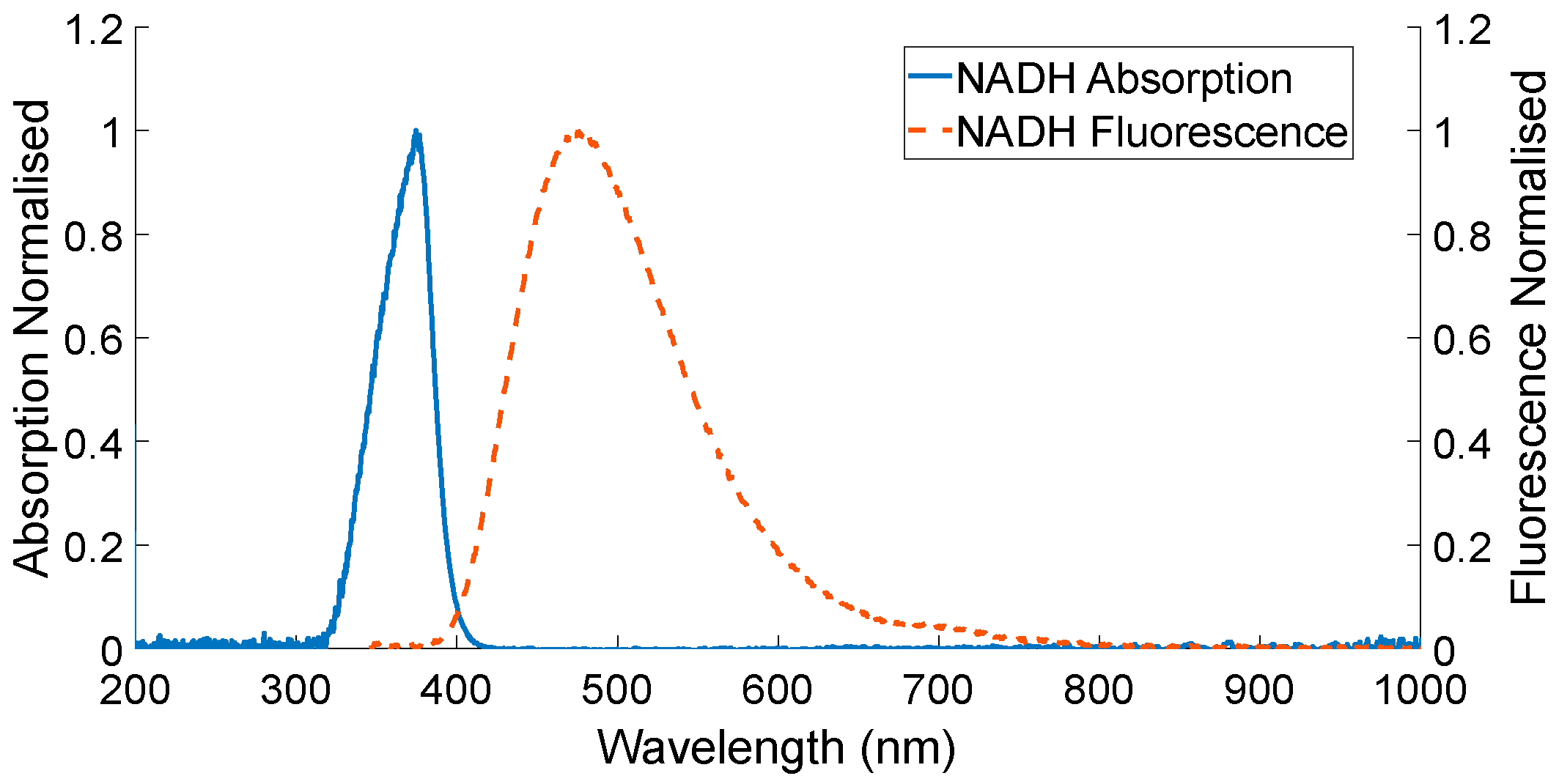
2. Bio-Photonics
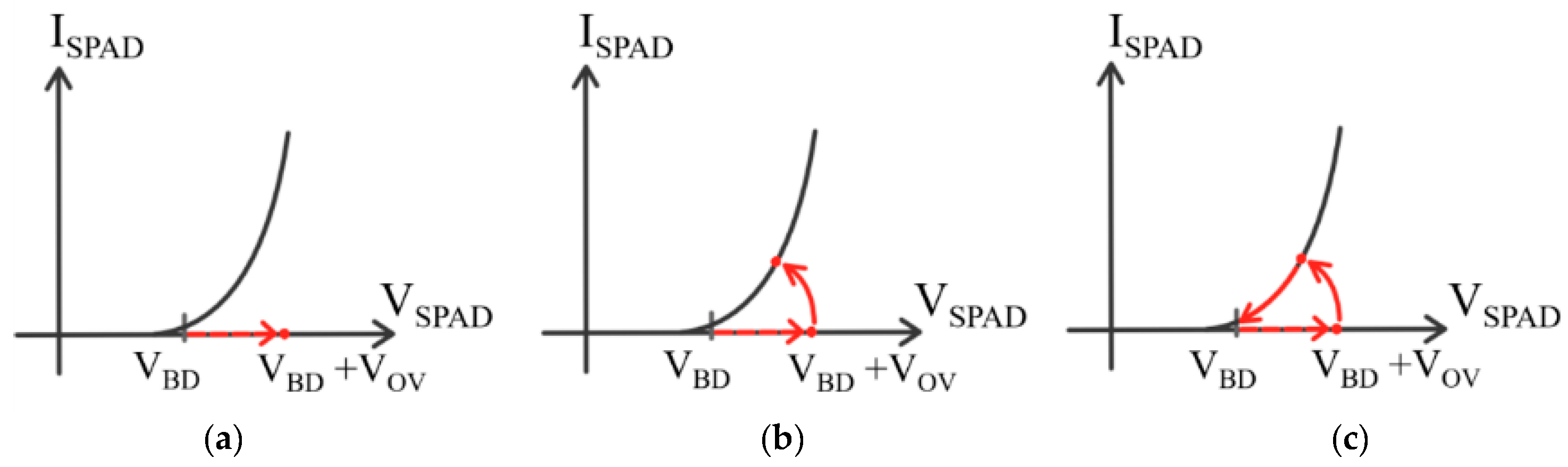
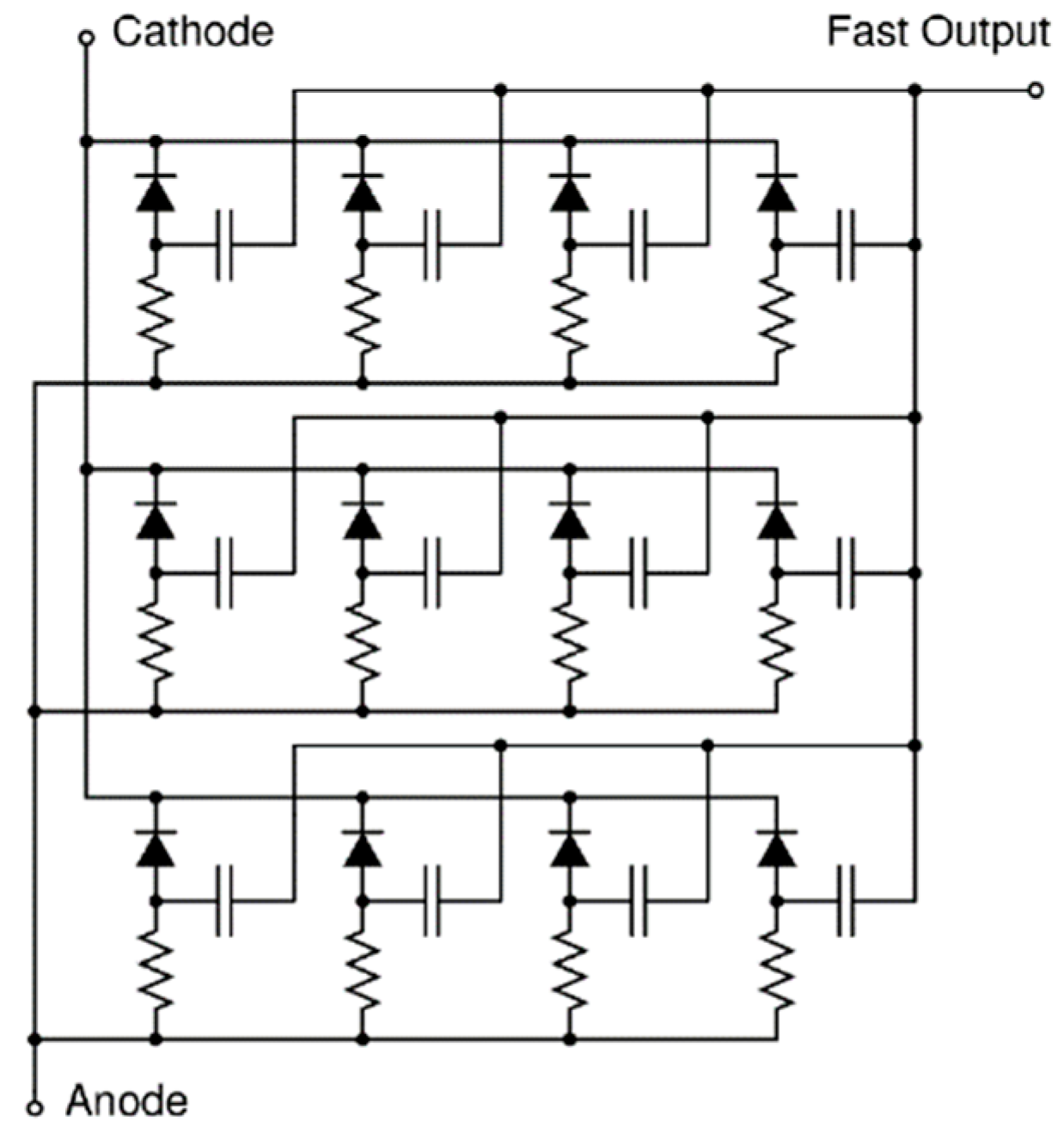
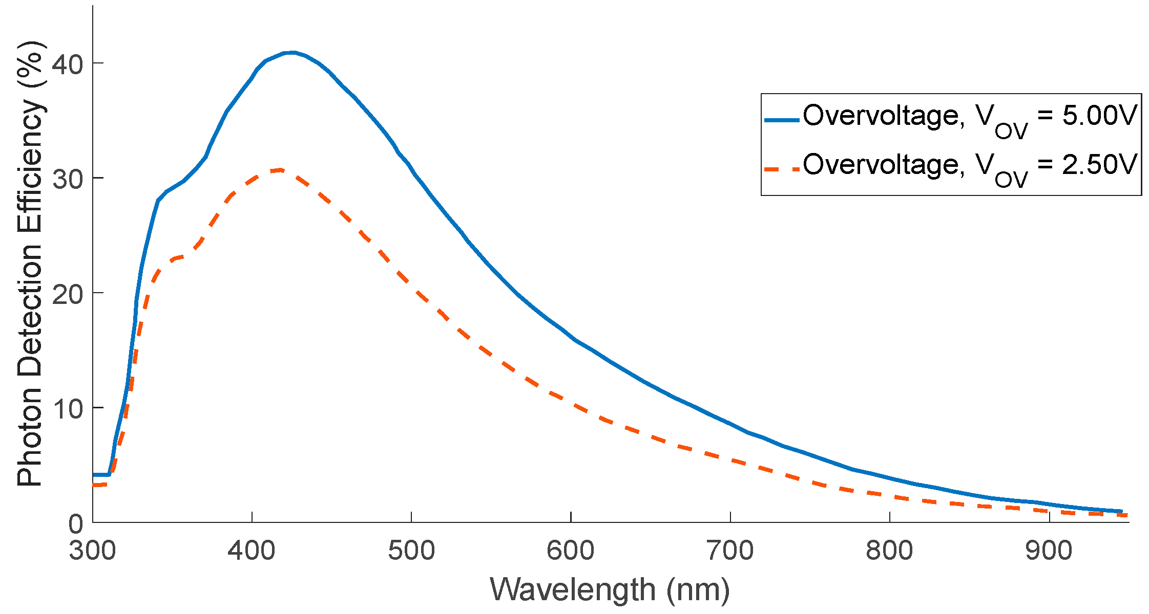
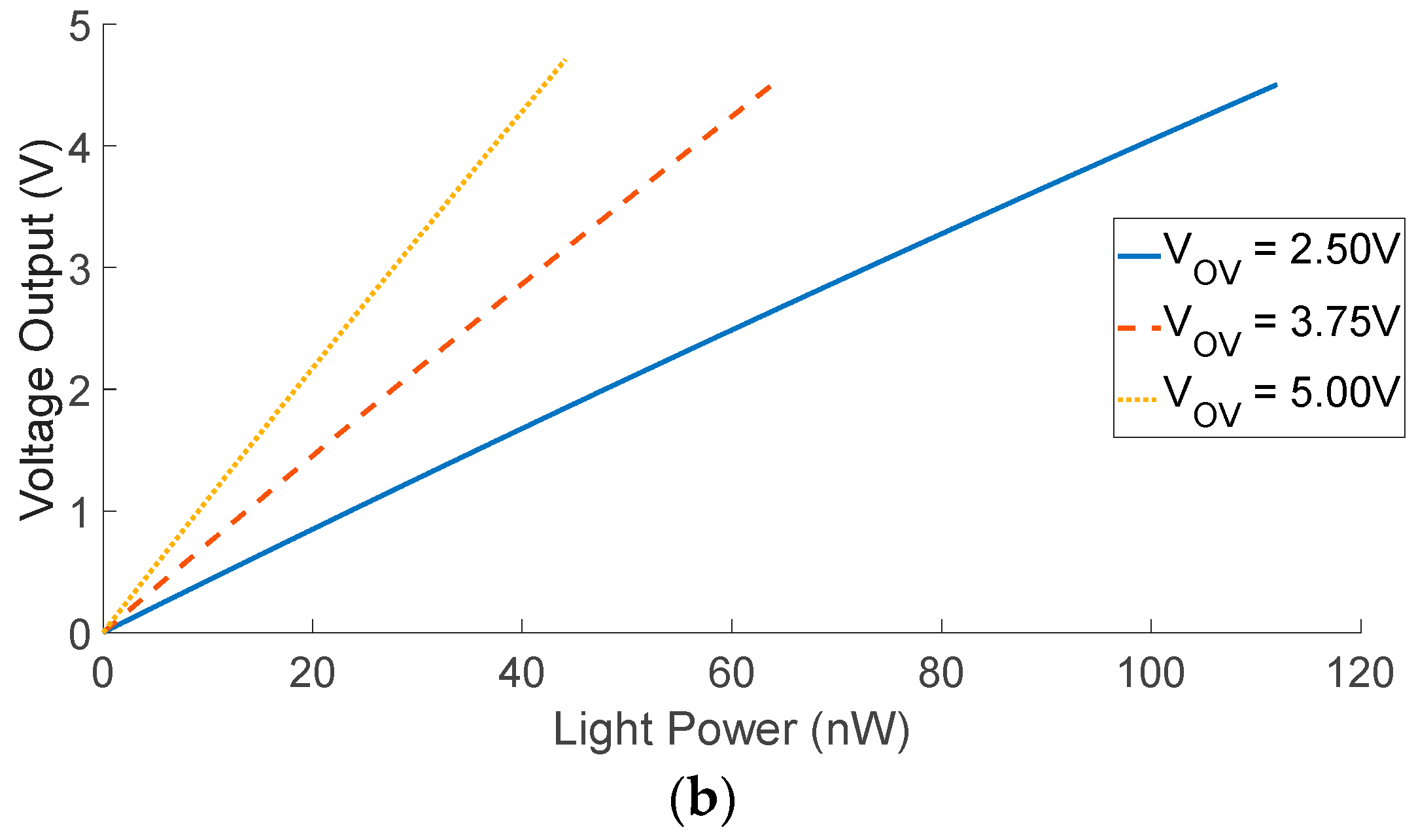
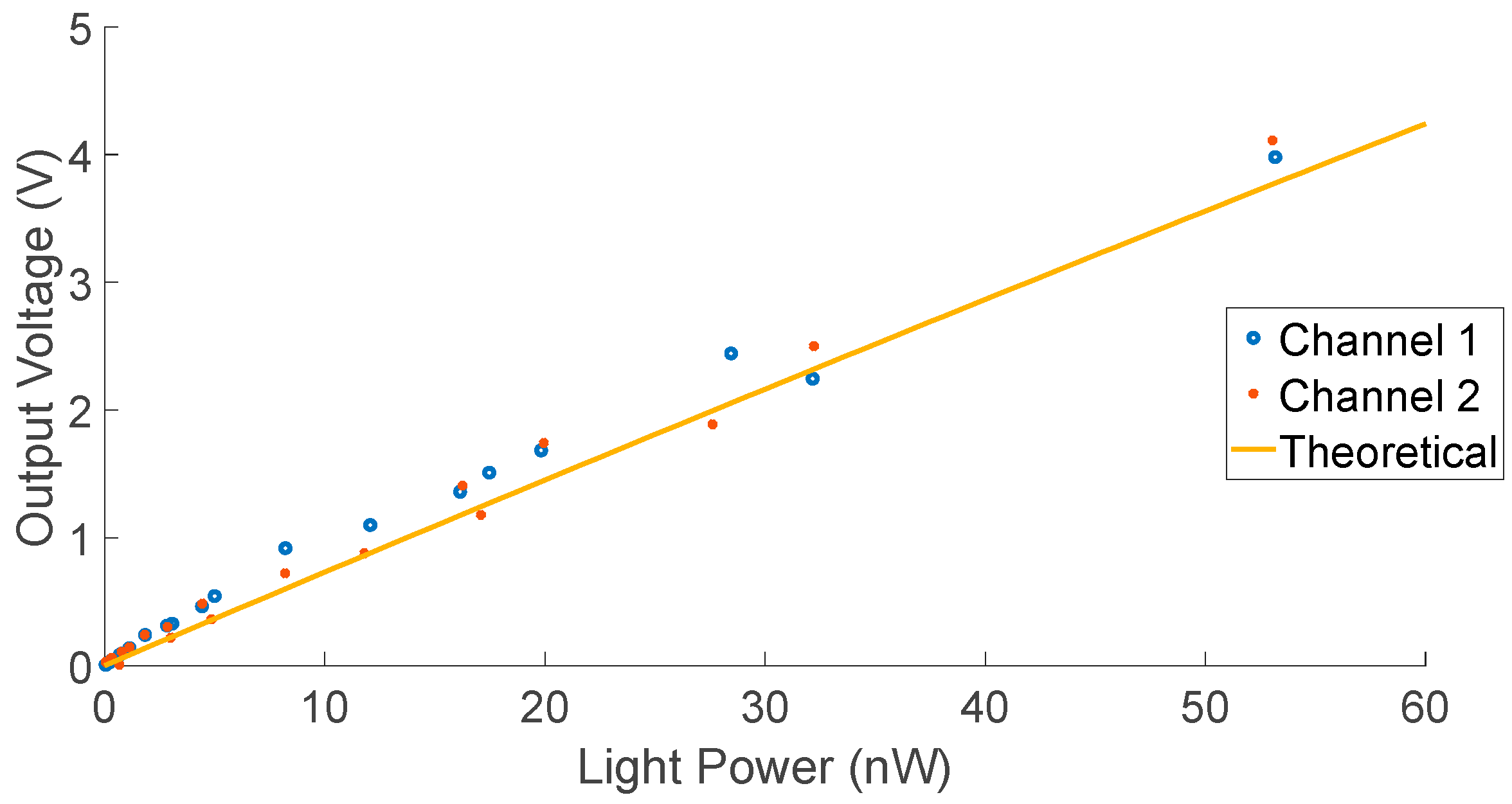
3. The Silicon Photomultiplier

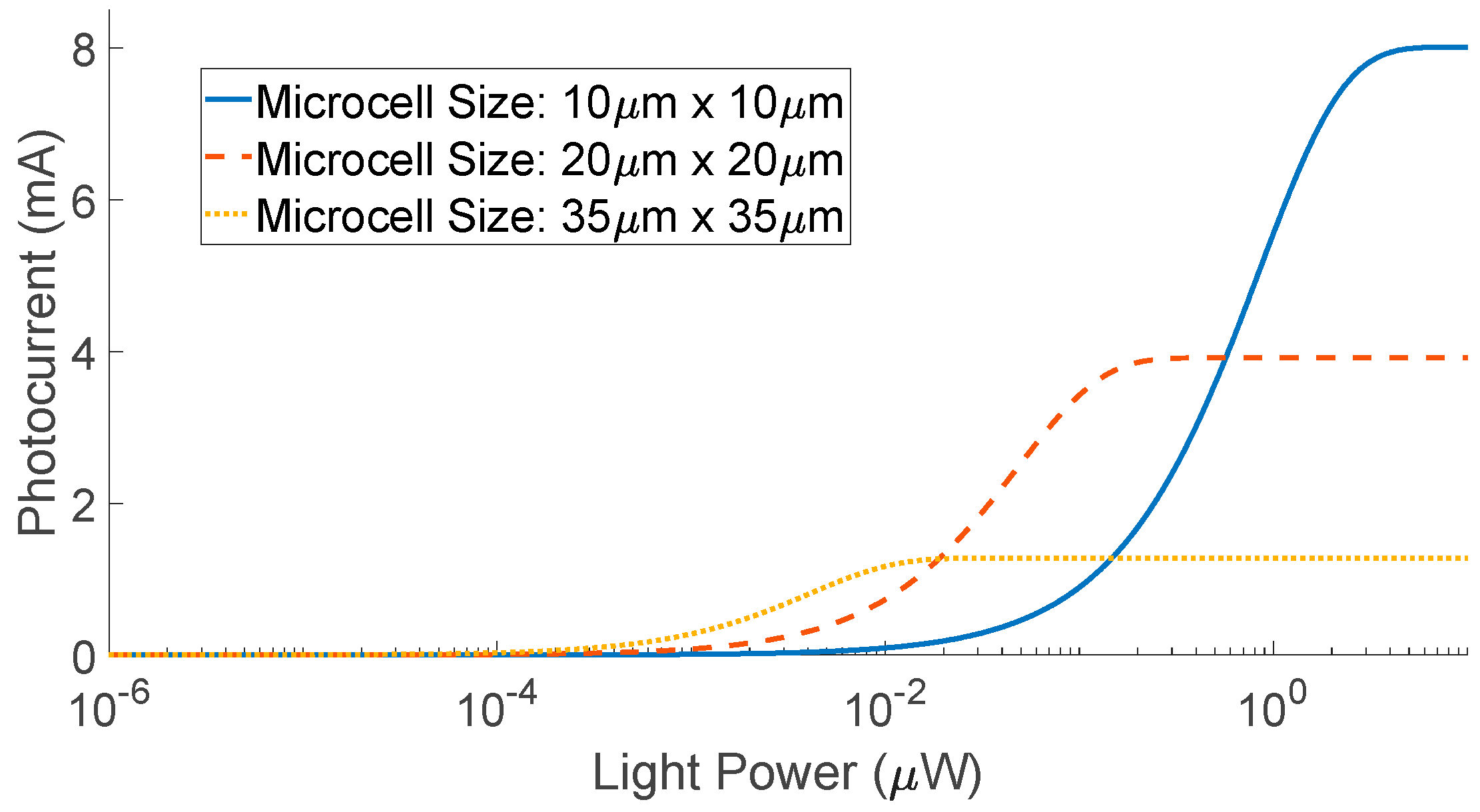
4. Detector Performance Comparison
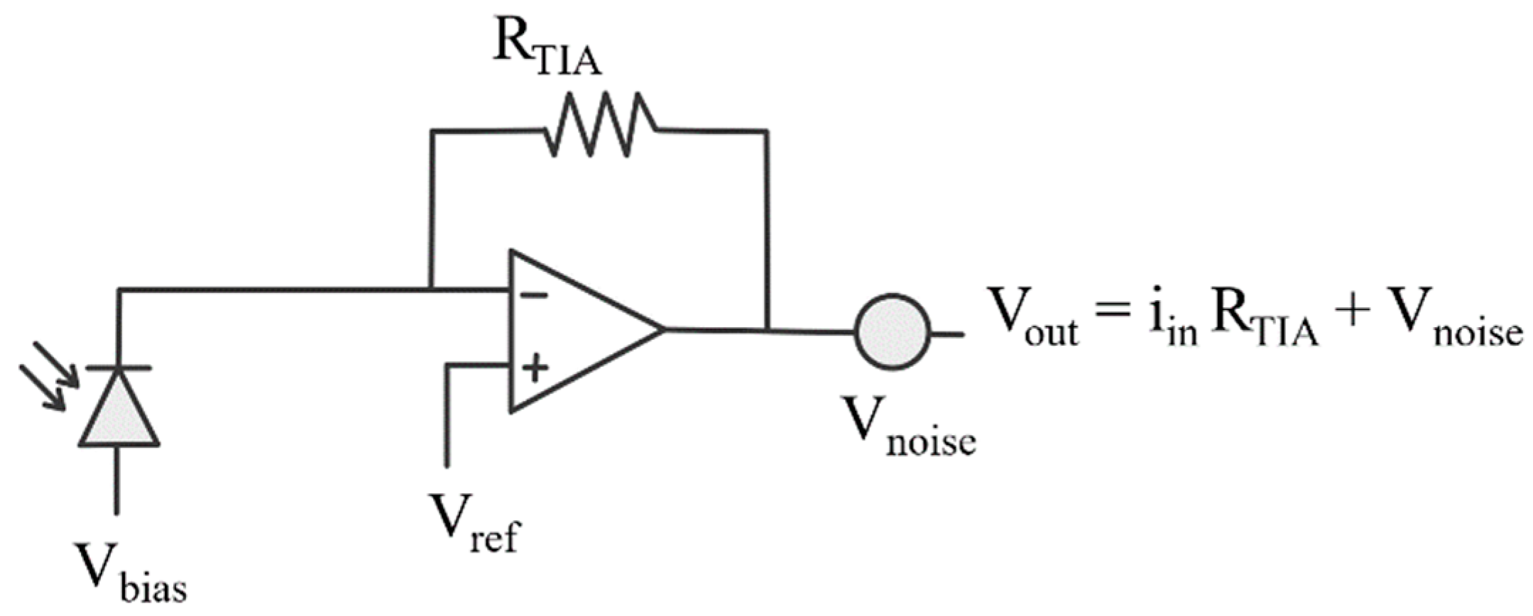
5. Readout Circuit Comparison
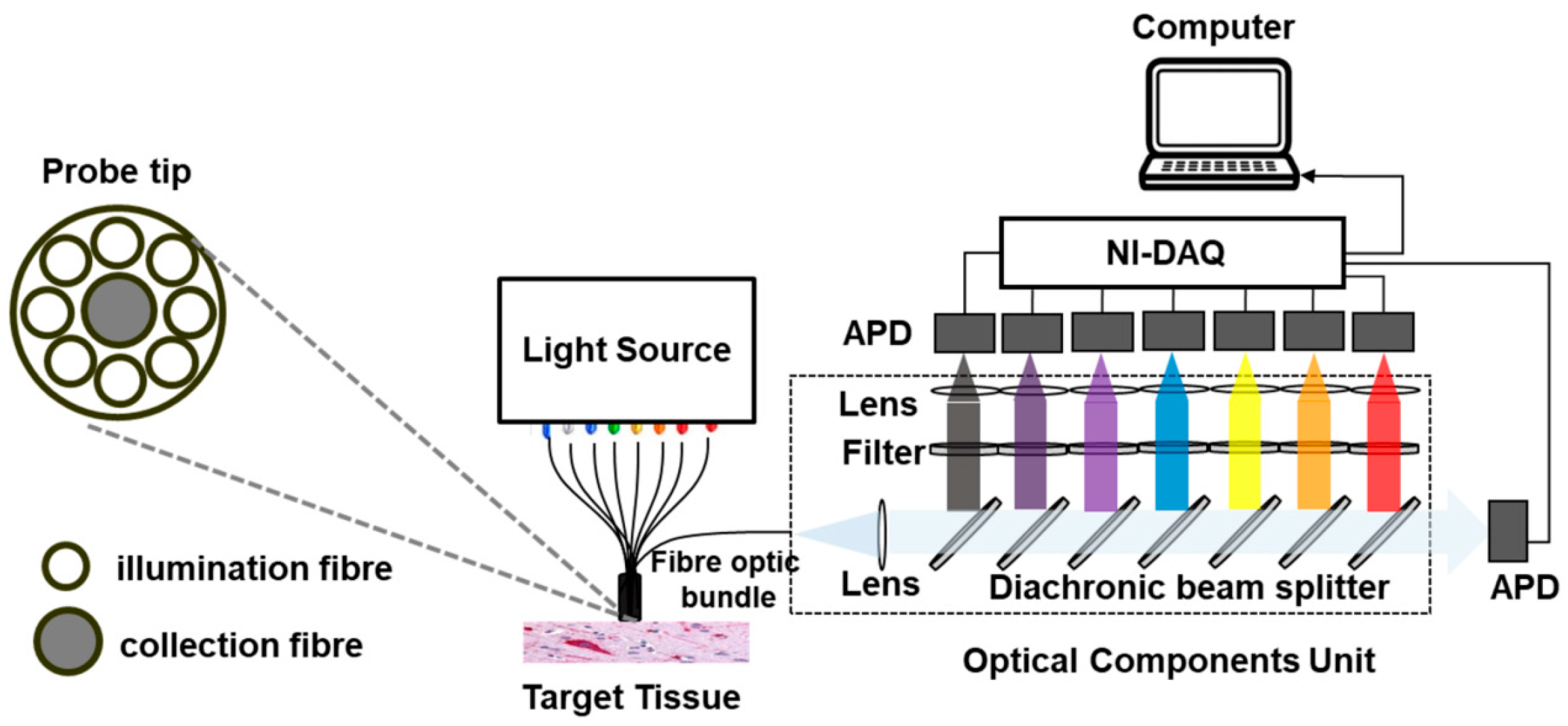
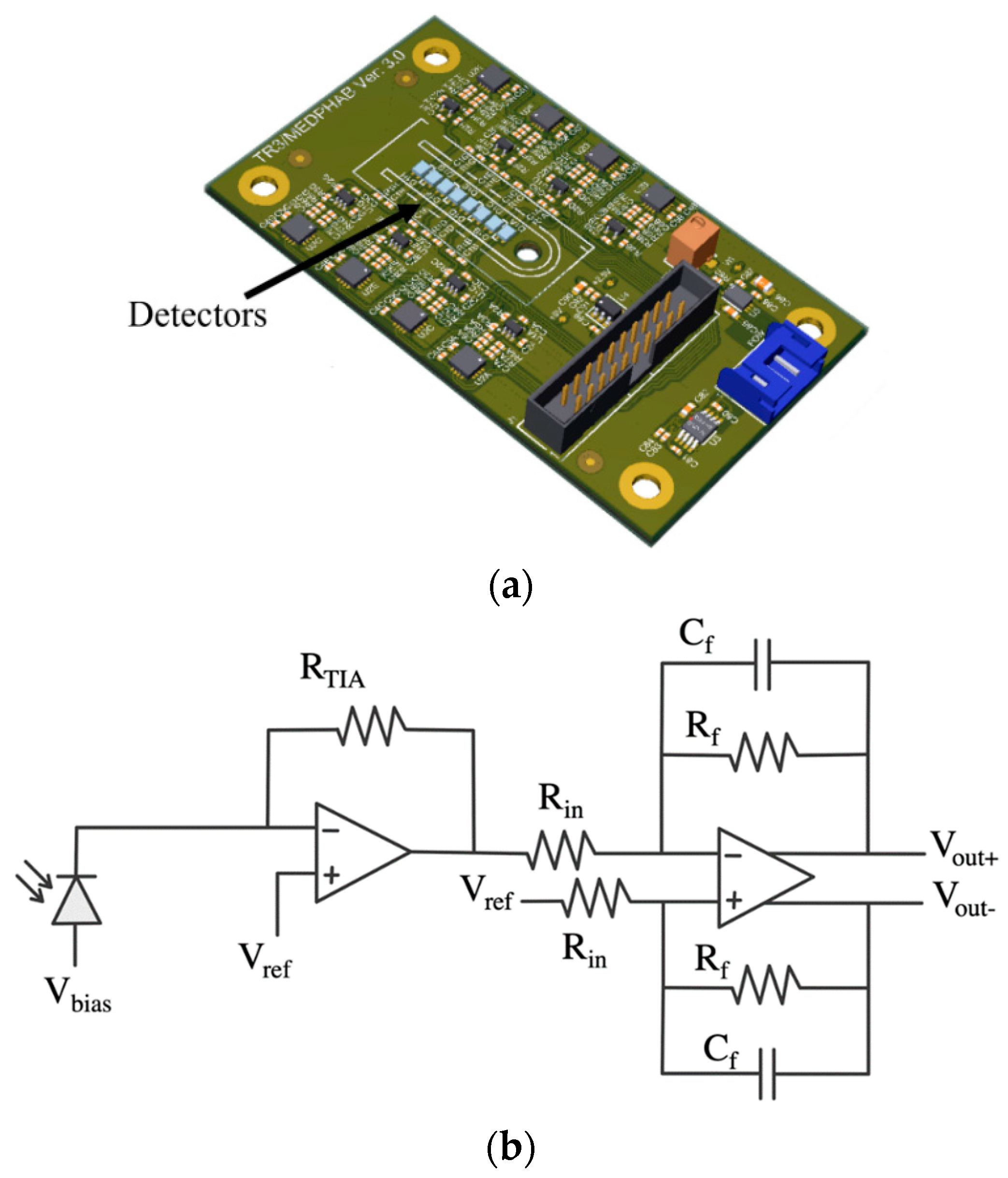
6. Use of Care: Tissue Recognition Project
7. Conclusions
Author Contributions
Funding
Institutional Review Board Statement
Informed Consent Statement
Data Availability Statement
Acknowledgments
Conflicts of Interest
References
- Tuchin, V. Tissue Optics and Photonics: Light-Tissue Interaction. J. Biomed. Photonics Eng. 2015, 1, 98–134. [Google Scholar] [CrossRef]
- Lu, H.; Grygoryev, K.; Bermingham, N.; Jansen, M.; O’Sullivan, M.; Nunan, G.; Buckley, K.; Manley, K.; Burke, R.; Andersson-Engels, S.; et al. Combined autofluorescence and diffuse reflectance for brain tumour surgical guidance: Initial ex vivo study results. Biomed. Opt. Express 2021, 12, 2432–2446. [Google Scholar] [CrossRef] [PubMed]
- Zhu, B.; Jaffer, F.A.; Ntziachristos, V.; Weissleder, R. Development of a near infrared fluorescence catheter: Operating characteristics and feasibility for atherosclerotic plaque detection. J. Phys. D Appl. Phys. 2005, 38, 2701–2707. [Google Scholar] [CrossRef]
- Grygoryev, K.; Lu, H.; Li, C.; Zhdanov, A.; Burke, R.; Andersson-Engels, S. Multi-Spectral Clinical Prototype for Fluorophore Detection. Front. Phys. 2021. [Google Scholar] [CrossRef]
- Croce, A.C.; Fiorani, S.; Locatelli, D.; Nano, R.; Ceroni, M.; Tancioni, F.; Giombelli, E.; Benericetti, E.; Bottiroli, G. Diagnostic Potential of Autofluorescence for an Assisted Intraoperative Delineation of Glioblastoma Resection Margins. Photochem. Photobiol. 2003, 77, 309–318. [Google Scholar] [CrossRef]
- Nogueira, M.S.; Maryam, S.; Amissah, M.; Lu, H.; Lynch, N.; Killeen, S.; O’Riordain, M.; Andersson-Engels, S. Evaluation of wavelength ranges and tissue depth probed by diffuse reflectance spectroscopy for colorectal cancer detection. Sci. Rep. 2021, 11, 798. [Google Scholar] [CrossRef] [PubMed]
- Gentile, F.; Das, G.; Coluccio, M.L.; Mecarini, F.; Accardo, A.; Tirinato, L.; Tallerico, R.; Cojoc, G.; Liberale, C.; Candeloro, P.; et al. Ultra low concentrated molecular detection using super hydrophobic surface based biophotonic devices. Microelectron. Eng. 2010, 87, 798–801. [Google Scholar] [CrossRef]
- Das, S.; Rehman, K.U.; Kao, F.-J. Signal Processing in Stimulated Emission Microscopy. In Proceedings of the 2019 IEEE International Conference on BioPhotonics (BioPhotonics), Taipei, Taiwan, 15–18 September 2019; pp. 1–2. [Google Scholar] [CrossRef]
- Grygoryev, K.; Komolibus, K.; Gunther, J.; Nunan, G.; Manley, K.; Andersson-Engels, S.; Burke, R. Cranial Perforation Using an Optically-Enhanced Surgical Drill. IEEE Trans. Biomed. Eng. 2020. [Google Scholar] [CrossRef] [PubMed]
- Xie, H.; Xie, Z.; Mousavi, M.; Bendsoe, N.; Brydegaard, M.; Axelsson, J.; Andersson-Engels, S. Design and validation of a fiber optic point probe instrument for therapy guidance and monitoring. J. Biomed. Opt. 2014, 19, 71408. [Google Scholar] [CrossRef] [Green Version]
- O’Sullivan, T.D.; Cerussi, A.E.; Cuccia, D.J.; Tromberg, B.J. Diffuse optical imaging using spatially and temporally modulated light. J. Biomed. Opt. 2012, 17, 071311. [Google Scholar] [CrossRef]
- Seo, J.; Kuyper, C.L.; Chiu, D.T.; Lee, L.P. Biophotonic MEMS for single molecule detection and manipulation. In Proceedings of the 2nd Annual International IEEE-EMBS Special Topic Conference on Microtechnologies in Medicine and Biology, Madison, WI, USA, 2–4 May 2002; Proceedings (Cat. No.02EX578). pp. 363–368. [Google Scholar] [CrossRef]
- Zhao, S.; Wu, X.; Chen, Y.; Wang, C.; Tang, Y. High gain avalanche photodiode (APD) arrays in flow cytometer opitical system. In Proceedings of the 2011 International Conference on Multimedia Technology, Hangzhou, China, 26–28 July 2011; pp. 2151–2153. [Google Scholar] [CrossRef]
- Sthalekar, C.C.; Miao, Y.; Koomson, V.J. Optical Characterization of Tissue Phantoms Using a Silicon Integrated fdNIRS System on Chip. IEEE Trans. Biomed. Circuits Syst. 2017, 11, 279–286. [Google Scholar] [CrossRef]
- Xiao, D.; Xiao, D.; Zang, Z.; Zang, Z.; Sapermsap, N.; Wang, Q.; Wang, Q.; Xie, W.; Xie, W.; Chen, Y.; et al. Dynamic fluorescence lifetime sensing with CMOS single-photon avalanche diode arrays and deep learning processors. Biomed. Opt. Express 2021, 12, 3450–3462. [Google Scholar] [CrossRef]
- Bisogni, M.G.; Del Guerra, A.; Belcari, N. Medical applications of silicon photomultipliers. Nucl. Instrum. Methods Phys. Res. Sect. Accel. Spectrometers Detect. Assoc. Equip. 2019, 926, 118–128. [Google Scholar] [CrossRef]
- Martinenghi, E.; Di Sieno, L.; Contini, D.; Sanzaro, M.; Pifferi, A.; Dalla Mora, A. Time-resolved single-photon detection module based on silicon photomultiplier: A novel building block for time-correlated measurement systems. Rev. Sci. Instrum. 2016, 87, 073101. [Google Scholar] [CrossRef] [PubMed]
- Tyndall, D.; Rae, B.R.; Li, D.D.-U.; Arlt, J.; Johnston, A.; Richardson, J.A.; Henderson, R.K. A High-Throughput Time-Resolved Mini-Silicon Photomultiplier With Embedded Fluorescence Lifetime Estimation in 0.13 μm CMOS. IEEE Trans. Biomed. Circuits Syst. 2012, 6, 562–570. [Google Scholar] [CrossRef] [PubMed]
- Kitsmiller, V.J.; Campbell, C.; O’Sullivan, T.D. Silicon Photomultipliers Increase Signal to Noise Ratio in Frequency Domain Diffuse Optical Spectroscopy of Human Muscle. In Proceedings of the Clinical and Translational Biophotonics 2020, Washington, DC, USA, 20–23 April 2020. Biophotonics Congress: Biomedical Optics 2020 (Translational, Microscopy, OCT, OTS, BRAIN), paper TTh4B.3. [Google Scholar]
- Sieno, L.D.; Pifferi, A.; Zouaoui, J.; Martinenghi, E.; Hervé, L.; Farina, A.; Derouard, J.; Dinten, J.-M.; Mora, A.D. Time-domain diffuse optical tomography using silicon photomultipliers: Feasibility study. J. Biomed. Opt. 2016, 21, 116002. [Google Scholar] [CrossRef] [PubMed]
- Muntean, A.; Venialgo, E.; Ardelean, A.; Sachdeva, A.; Ripiccini, E.; Palubiak, D.; Jackson, C.; Charbon, E. Blumino: The First Fully Integrated Analog SiPM with On-Chip Time Conversion. IEEE Trans. Radiat. Plasma Med. Sci. 2021, 5, 671–678. [Google Scholar] [CrossRef]
- Corsi, F.; Foresta, M.; Marzocca, C.; Matarrese, G.; Guerra, A.D. ASIC development for SiPM readout. J. Instrum. 2009, 4, P03004. [Google Scholar] [CrossRef]
- Bouchel, M.; Callier, S.; Dulucq, F.; Fleury, J.; Jaeger, J.-J.; de L. Taille, C.; Martin-Chassard, G.; Raux, L. SPIROC (SiPM Integrated Read-Out Chip): Dedicated very front-end electronics for an ILC prototype hadronic calorimeter with SiPM read-out. J. Instrum. 2011, 6, C01098. [Google Scholar] [CrossRef]
- Evers, D.J.; Nachabé, R.; Hompes, D.; van Coevorden, F.; Lucassen, G.W.; Hendriks, B.H.W.; van Velthuysen, M.-L.F.; Wesseling, J.; Ruers, T.J.M. Optical sensing for tumor detection in the liver. Eur. J. Surg. Oncol. 2013, 39, 68–75. [Google Scholar] [CrossRef] [PubMed]
- Tanis, E.; Evers, D.J.; Spliethoff, J.W.; Pully, V.V.; Kuhlmann, K.; van Coevorden, F.; Hendriks, B.H.W.; Sanders, J.; Prevoo, W.; Ruers, T.J.M. In Vivo tumor identification of colorectal liver metastases with diffuse reflectance and fluorescence spectroscopy. Lasers Surg. Med. 2016, 48, 820–827. [Google Scholar] [CrossRef]
- Baltussen, E.J.M.; Snæbjörnsson, P.; de Koning, S.G.B.; Sterenborg, H.J.C.M.; Aalbers, A.G.J.; Kok, N.; Beets, G.L.; Hendriks, B.H.W.; Kuhlmann, K.F.D.; Ruers, T.J.M. Diffuse reflectance spectroscopy as a tool for real-time tissue assessment during colorectal cancer surgery. J. Biomed. Opt. 2017, 22, 106014. [Google Scholar] [CrossRef]
- Langhout, G.C.; Spliethoff, J.W.; Schmitz, S.J.; Aalbers, A.G.J.; van Velthuysen, M.-L.F.; Hendriks, B.H.W.; Ruers, T.J.M.; Kuhlmann, K.F.D. Differentiation of healthy and malignant tissue in colon cancer patients using optical spectroscopy: A tool for image-guided surgery. Lasers Surg. Med. 2015, 47, 559–565. [Google Scholar] [CrossRef] [PubMed]
- de Boer, L.L.; Bydlon, T.M.; van Duijnhoven, F.; Vranken Peeters, M.-J.T.F.D.; Loo, C.E.; Winter-Warnars, G.A.O.; Sanders, J.; Sterenborg, H.J.C.M.; Hendriks, B.H.W.; Ruers, T.J.M. Towards the use of diffuse reflectance spectroscopy for real-time in vivo detection of breast cancer during surgery. J. Transl. Med. 2018, 16, 367. [Google Scholar] [CrossRef] [PubMed]
- de Koning, S.G.B.; Baltussen, E.J.M.; Karakullukcu, M.B.; Dashtbozorg, B.; Smit, L.A.; Dirven, R.; Hendriks, B.H.W.; Sterenborg, H.J.C.M.; Ruers, T.J.M. Toward complete oral cavity cancer resection using a handheld diffuse reflectance spectroscopy probe. J. Biomed. Opt. 2018, 23, 121611. [Google Scholar] [CrossRef]
- Dremin, V.; Potapova, E.; Zherebtsov, E.; Kandurova, K.; Shupletsov, V.; Alekseyev, A.; Mamoshin, A.; Dunaev, A. Optical percutaneous needle biopsy of the liver: A pilot animal and clinical study. Sci. Rep. 2020, 10, 14200. [Google Scholar] [CrossRef]
- Kiesel, B.; Freund, J.; Reichert, D.; Wadiura, L.; Erkkilae, M.T.; Woehrer, A.; Hervey-Jumper, S.; Berger, M.S.; Widhalm, G. 5-ALA in Suspected Low-Grade Gliomas: Current Role, Limitations, and New Approaches. Front. Oncol. 2021, 11. Available online: https://www.frontiersin.org/article/10.3389/fonc.2021.699301 (accessed on 23 March 2022). [CrossRef]
- Jaber, M.; Ewelt, C.; Wölfer, J.; Brokinkel, B.; Thomas, C.; Hasselblatt, M.; Grauer, O.; Stummer, W. Is Visible Aminolevulinic Acid-Induced Fluorescence an Independent Biomarker for Prognosis in Histologically Confirmed (World Health Organization 2016) Low-Grade Gliomas? Neurosurgery 2019, 84, 1214–1224. [Google Scholar] [CrossRef]
- Haj-Hosseini, N.; Richter, J.; Andersson-Engels, S.; Wårdell, K. Photobleaching behavior of protoporphyrin IX during 5-aminolevulinic acid marked glioblastoma detection. Proc. SPIE 2009, 7161. [Google Scholar] [CrossRef]
- Andersson-Engels, S.; Klinteberg, C.; Svanberg, K.; Svanberg, S. In Vivo fluorescence imaging for tissue diagnostics. Phys. Med. Biol. 1997, 42, 815–824. [Google Scholar] [CrossRef]
- Croce, A.C.; Bottiroli, G. Autofluorescence Spectroscopy and Imaging: A Tool for Biomedical Research and Diagnosis. Eur. J. Histochem. 2014, 58, 2461. [Google Scholar] [CrossRef] [PubMed]
- de Veld, D.C.G.; Skurichina, M.; Witjes, M.J.H.; Duin, R.P.W.; Sterenborg, H.J.C.M.; Roodenburg, J.L.N. Autofluorescence and diffuse reflectance spectroscopy for oral oncology. Lasers Surg. Med. 2005, 36, 356–364. [Google Scholar] [CrossRef] [PubMed]
- Keller, M.D.; Majumder, S.K.; Kelley, M.C.; Meszoely, I.M.; Boulos, F.I.; Olivares, G.M.; Mahadevan-Jansen, A. Autofluorescence and diffuse reflectance spectroscopy and spectral imaging for breast surgical margin analysis. Lasers Surg. Med. 2010, 42, 15–23. [Google Scholar] [CrossRef]
- Breslin, T.M.; Xu, F.; Palmer, G.M.; Zhu, C.; Gilchrist, K.W.; Ramanujam, N. Autofluorescence and diffuse reflectance properties of malignant and benign breast tissues. Ann. Surg. Oncol. 2004, 11, 65–70. [Google Scholar] [CrossRef] [PubMed]
- Krafft, C.; Popp, J. Medical needs for translational biophotonics with the focus on Raman-based methods. Transl. Biophotonics 2019, 1, e201900018. [Google Scholar] [CrossRef]
- Hanlon, E.B.; Manoharan, R.; Koo, T.W.; Shafer, K.E.; Motz, J.T.; Fitzmaurice, M.; Kramer, J.R.; Itzkan, I.; Dasari, R.R.; Feld, M.S. Prospects for in vivo Raman spectroscopy. Phys. Med. Biol. 2000, 45, R1-59. [Google Scholar] [CrossRef]
- Movasaghi, Z.; Rehman, S.; Rehman, I.U. Raman Spectroscopy of Biological Tissues. Appl. Spectrosc. Rev. 2007, 42, 493–541. [Google Scholar] [CrossRef]
- Majumder, S.K.; Keller, M.D.; Boulos, F.I.; Kelley, M.C.; Mahadevan-Jansen, A. Comparison of autofluorescence, diffuse reflectance, and Raman spectroscopy for breast tissue discrimination. J. Biomed. Opt. 2008, 13, 054009. [Google Scholar] [CrossRef]
- Krafft, C.; Schmitt, M.; Schie, I.W.; Cialla-May, D.; Matthäus, C.; Bocklitz, T.; Popp, J. Label-Free Molecular Imaging of Biological Cells and Tissues by Linear and Nonlinear Raman Spectroscopic Approaches. Angew. Chem. Int. Ed. Engl. 2017, 56, 4392–4430. [Google Scholar] [CrossRef]
- Aubertin, K.; Trinh, V.Q.; Jermyn, M.; Baksic, P.; Grosset, A.-A.; Desroches, J.; St-Arnaud, K.; Birlea, M.; Vladoiu, M.C.; Latour, M.; et al. Mesoscopic characterization of prostate cancer using Raman spectroscopy: Potential for diagnostics and therapeutics. BJU Int. 2018, 122, 326–336. [Google Scholar] [CrossRef]
- Bruschini, C.; Homulle, H.; Antolovic, I.M.; Burri, S.; Charbon, E. Single-photon avalanche diode imagers in biophotonics: Review and outlook. Light Sci. Appl. 2019, 8, 87. [Google Scholar] [CrossRef] [PubMed]
- Piron, F.; Morrison, D.; Yuce, M.R.; Redouté, J.-M. A Review of Single-Photon Avalanche Diode Time-of-Flight Imaging Sensor Arrays. IEEE Sens. J. 2021, 21, 12654–12666. [Google Scholar] [CrossRef]
- Shukla, R.A.; Achanta, V.G.; Dugad, S.R.; Duttagupta, S.P.; Gupta, S.K.; Prabhu, S.S. Design and simulation of silicon photo-multiplier. In Proceedings of the 2016 3rd International Conference on Emerging Electronics (ICEE), Mumbai, India, 27–30 December 2016; pp. 1–4. [Google Scholar]
- Piemonte, C.; Gola, A. Overview on the main parameters and technology of modern Silicon Photomultipliers. Nucl. Instrum. Methods Phys. Res. Sect. Accel. Spectrometers Detect. Assoc. Equip. 2019, 926, 2–15. [Google Scholar] [CrossRef]
- Klanner, R. Characterisation of SiPMs. Nucl. Instrum. Methods Phys. Res. Sect. Accel. Spectrometers Detect. Assoc. Equip. 2019, 926, 36–56. [Google Scholar] [CrossRef]
- Silicon Photomultipliers (SiPM), Low Noise, Blue-Sensitive. C-Series SiPM Sensors. Available online: https://www.onsemi.com/pdf/datasheet/microc-series-d.pdf (accessed on 10 March 2020).
- Gallina, G.; Retière, F.; Giampa, P.; Kroeger, J.; Margetak, P.; Byrne Mamahit, S.; de S. Croix, A.; Edaltafar, A.; Martin, L.; Massacret, N.; et al. Characterization of SiPM Avalanche Triggering Probabilities. IEEE Trans. Electron. Devices 2019, 66, 4228–4234. [Google Scholar] [CrossRef]
- Low Breakdown Voltage, Wide Dynamic Range Type MPPC with Small Pixels. Available online: https://www.hamamatsu.com/resources/pdf/ssd/s14160-1310ps_etc_kapd1070e.pdf (accessed on 15 September 2020).
- RGB SiPMs. Available online: https://advansid.com/attachment/get/up_54_1432741139.pdf (accessed on 10 April 2022).
- NUV SiPMs. Available online: https://advansid.com/attachment/get/up_54_1432731416.pdf (accessed on 10 April 2022).
- SFH2704 Silicon PIN Photodiode. Available online: https://www.mouser.com/datasheet/2/311/OSRAM-12-12-2018-SFH_2704_EN-1509916.pdf (accessed on 24 June 2021).
- Short Wavelength Type APD, for 600 nm Band. Available online: https://www.hamamatsu.com/resources/pdf/ssd/s12053-02_etc_kapd1001e.pdf (accessed on 10 April 2022).
- Rosado, J.; Aranda, V.M.; Blanco, F.; Arqueros, F. Modeling crosstalk and afterpulsing in silicon photomultipliers. Nucl. Instrum. Methods Phys. Res. Sect. Accel. Spectrometers Detect. Assoc. Equip. 2015, 787, 153–156. [Google Scholar] [CrossRef]
- Finocchiaro, P.; Pappalardo, A.; Cosentino, L.; Belluso, M.; Billotta, S.; Bonanno, G.; di Mauro, S. Features of Silicon Photo Multipliers: Precision Measurements of Noise, Cross-Talk, Afterpulsing, Detec-tion Efficiency. IEEE Trans. Nucl. Sci. 2009, 56, 1033–1041. [Google Scholar] [CrossRef]
- Kitsmiller, V.J.; Campbell, C.; O’Sullivan, T.D. Optimizing sensitivity and dynamic range of silicon photomultipliers for frequency-domain near infrared spectroscopy. Biomed. Opt. Express 2020, 11, 5373–5387. [Google Scholar] [CrossRef] [PubMed]
- Acerbi, F.; Gundacker, S. Understanding and simulating SiPMs. Nucl. Instrum. Methods Phys. Res. Sect. Accel. Spectrometers Detect. Assoc. Equip. 2019, 926, 16–35. [Google Scholar] [CrossRef]
- Saraswathy, A.; Jayasree, R.S.; Baiju, K.V.; Gupta, A.K.; Pillai, V.P.M. Optimum Wavelength for the Differentiation of Brain Tumor Tissue Using Autofluorescence Spectroscopy. Photomed. Laser Surg. 2009, 27, 425–433. [Google Scholar] [CrossRef] [Green Version]


| Diffuse Reflectance | Auto-Fluorescence | Raman Spectroscopy | |
|---|---|---|---|
| Optical Power (W) | 1–10 μ | 10–100 n | 1–10 p |
| OnSemi [50] (MicroFC-10010) | Hamamatsu [52] (S14160-1310PS) | Hamamatsu [52] (S14160-1315PS) | AdvanSid [53] (ASD-RGB1S-P) | AdvanSid [54] (ASD-NUV1S-P) | |
|---|---|---|---|---|---|
| Gain | 2 × 10⁵ | 1.8 × 10⁵ | 3.6 × 10⁵ | 2.7 × 10⁶ | 3.6 × 10⁶ |
| Operational Bias (V) | 24.2–24.7 | 35–41 | 35–41 | 27–29 | 26–28 |
| Overvoltage (V) | 1–5 | 5 | 4 | 2–4 | 2–6 |
| Spectral Range (nm) | 300 to 950 | 290 to 900 | 290 to 900 | 350 to 900 | 350 to 900 |
| Peak Sensitivity (nm) | 420 | 460 | 460 | 550 | 420 |
| PDE (%) | 14 | 18 | 32 | 32.5 | 43 |
| Cell Capacitance (fF) | 12.8 | 5.8 | 14.4 | 90 | 90 |
| Area (mm × mm) | 2.394 | 5.523 | 5.523 | 5.034 | 5.034 |
| Active Area (mm × mm) | 1 × 1 | 1.3 × 1.3 | 1.3 × 1.3 | 1 × 1 | 1 × 1 |
| Microcell Size (μm) | 10 × 10 | 10 × 10 | 15 × 15 | 40 × 40 | 40 × 40 |
| PIN [55] (SFH2704) | APD [56] (S12053-05) | SiPM [50] (C10010) | |
|---|---|---|---|
| Gain | 1 | 1–50 | 2 × 10⁵ |
| Output Type | Analogue | Analogue | Analogue or Digital |
| Operational Bias (V) | 6 | 150–200 | 24.2–24.7 |
| Overvoltage (V) | – | – | 1–5 |
| Spectral Range (nm) | 400 to 1100 | 200 to 1000 | 300 to 950 |
| Peak Sensitivity (nm) | 900 | 620 | 420 * |
| PDE/QE (%) | – | 80 | 18 ** |
| Capacitance (pF) | 13.4 | 5 | 50 |
| Max Photocurrent (μA) | 1.22 | 84 | 16 × 103 |
| Dark Current (nA) | 0.1–25 | 0.2–5 | 1–10 |
| Area (mm2) | 3.6 | 21.24 | 2.4 |
| Active Area (mm2) | 1.51 | 7.07 | 1 |
| Responsivity (A/W) | 0.34 | 21 | 4 × 10³ |
| Rise Time (ns) | 47 | 0.875 | 0.3 |
| Min Detection Optical Power (pW) | 73.53 × 10³ | 399 | 2.5 |
| Max Detection Optical Power (μW) | 4.41 | 16 | 1 |
| Optical Dynamic Range (dB) | 17.78 | 46.03 | 56 |
| Single Photon Detection | No | No | Yes |
| Photon Time Stamping | No | No | Yes |
Publisher’s Note: MDPI stays neutral with regard to jurisdictional claims in published maps and institutional affiliations. |
© 2022 by the authors. Licensee MDPI, Basel, Switzerland. This article is an open access article distributed under the terms and conditions of the Creative Commons Attribution (CC BY) license (https://creativecommons.org/licenses/by/4.0/).
Share and Cite
Georgel, R.; Grygoryev, K.; Sorensen, S.; Lu, H.; Andersson-Engels, S.; Burke, R.; O'Hare, D. Silicon Photomultiplier—A High Dynamic Range, High Sensitivity Sensor for Bio-Photonics Applications. Biosensors 2022, 12, 793. https://doi.org/10.3390/bios12100793
Georgel R, Grygoryev K, Sorensen S, Lu H, Andersson-Engels S, Burke R, O'Hare D. Silicon Photomultiplier—A High Dynamic Range, High Sensitivity Sensor for Bio-Photonics Applications. Biosensors. 2022; 12(10):793. https://doi.org/10.3390/bios12100793
Chicago/Turabian StyleGeorgel, Rachel, Konstantin Grygoryev, Simon Sorensen, Huihui Lu, Stefan Andersson-Engels, Ray Burke, and Daniel O'Hare. 2022. "Silicon Photomultiplier—A High Dynamic Range, High Sensitivity Sensor for Bio-Photonics Applications" Biosensors 12, no. 10: 793. https://doi.org/10.3390/bios12100793