3.4. Re-Anodising in Chromic Acid—Film Morphology
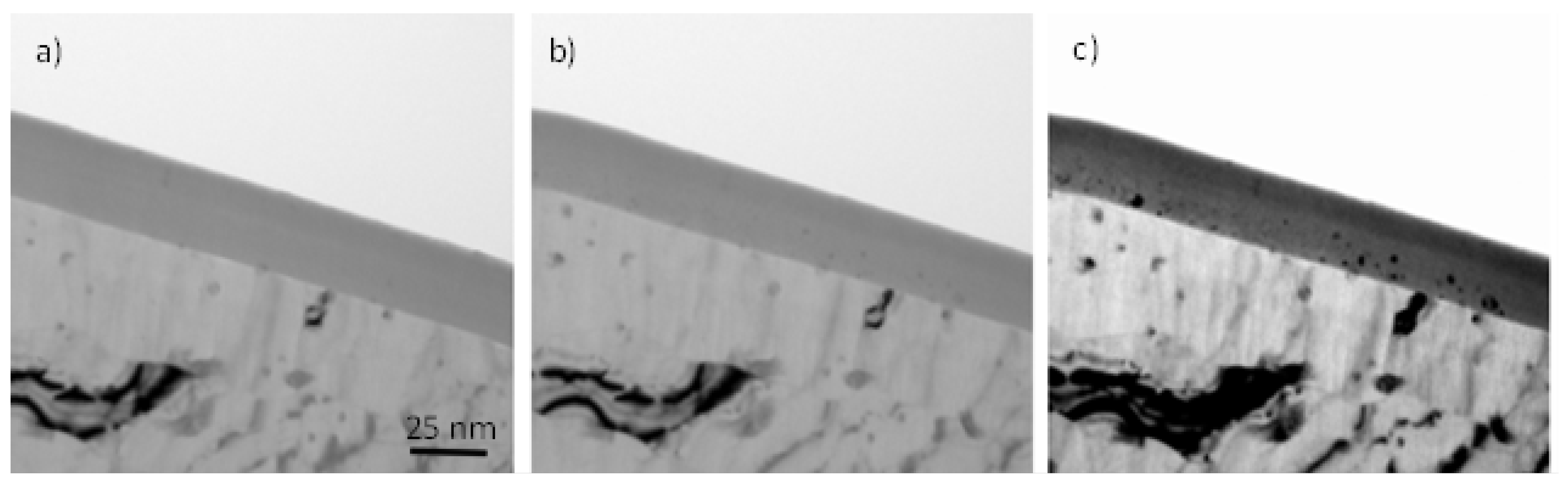
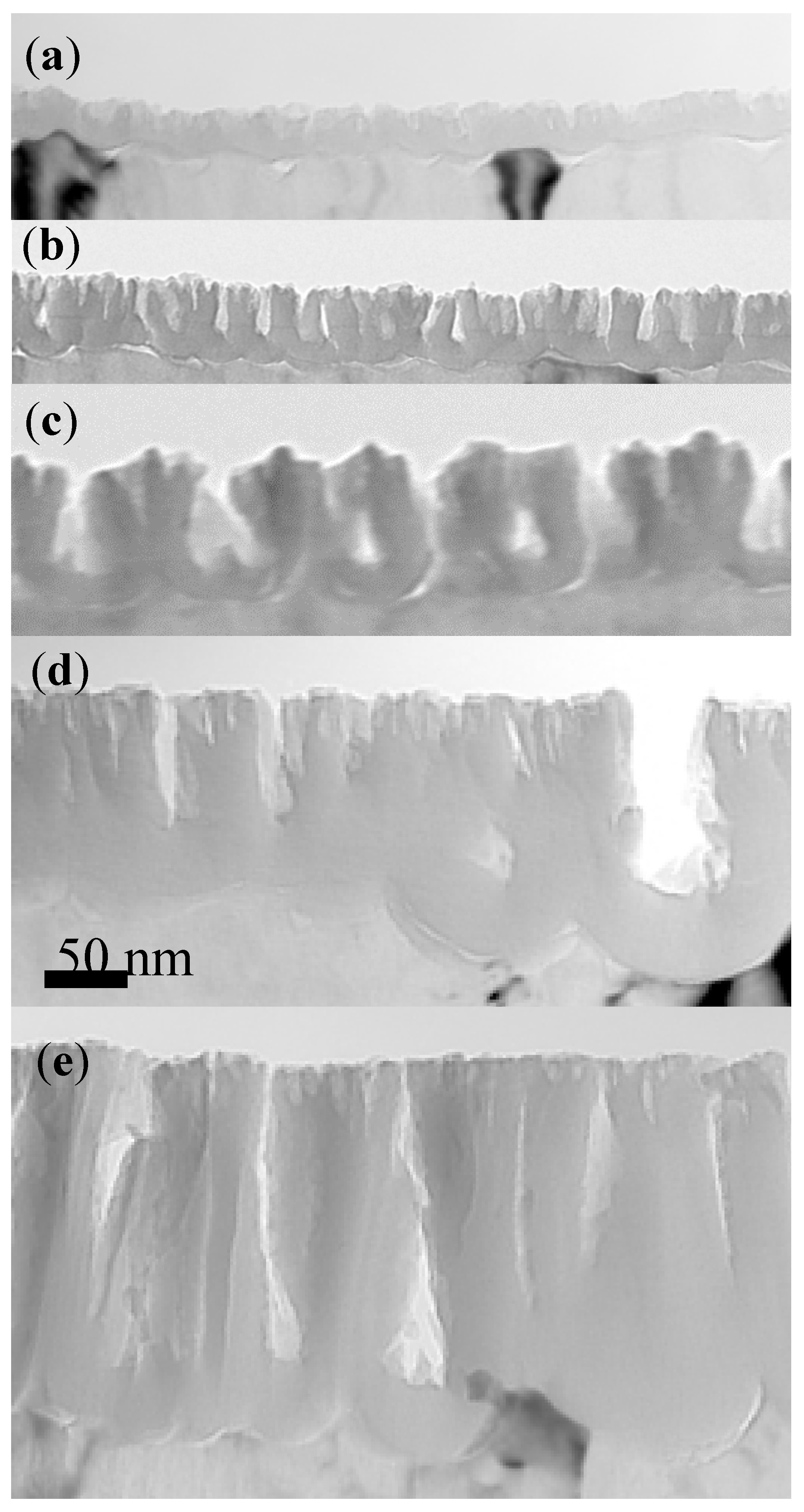
Figure 3 shows the transmission electron micrographs of ultramicrotomed cross-sections of specimens formed in CR18 (sample CrRef), and then re-anodized in CR16 for 30 s (Cr30), 60 s (sample Cr60), 120 s (sample Cr120), and 300 s (sample Cr300). The CrRef sample of a total thickness of 31 ± 2 nm consists of a barrier region (19 ± 2 nm) and a porous region (12 ± 2 nm). The anodic films of samples re-anodised in CR16 also consist of a barrier region and a porous region, with average total thicknesses of 62 ± 3 nm, 91 ± 4 nm, 159 ± 6, and 285 ± 15 nm; the barrier region thickness increases gradually from 19 nm (CrRef) to 23 ± 2 nm (Cr30), 21 ± 2 nm (Cr60), 23.8 ± 2 nm (Cr120), and 25 ± 2 nm (Cr300). The thick outer pore region contains fine pores near the film surface formed soon after the start of anodising.
The morphology of the major pores is similar to so-called feather-like pores, which are also observed for films formed in borax electrolyte [
19]. The accuracy of the thicknesses is ~7% due to the irregular scalloping of the Al/Al
2O
3 interface and uncertainty in the location of the section with respect to the centre of the pores. The average growth rate of the anodic film is 1.13 nm/s, higher than in the Ar18–Cr16 experiment (average 1.0 nm/s). This agrees with the calculated thickness of Al oxidised from the charge passed through the cell, assuming the formation of Al
3+ ions [
25,
26] during anodising at 3 mA/cm
2. The charges passed in the cell during re-anodising can oxidise 29, 57, 120, and 275 nm of Al. The volume expansion factors on converting the aluminium to oxide (the ratio of the thickness gained determined from TEM and the thickness of aluminium oxidised calculated from the charge passed through the cell) are 1.06 ± 0.1, 1.0 ± 0.045, 1.06 ± 0.06, and 1.02 ± 0.02, respectively, and 1.08 for CrRef.
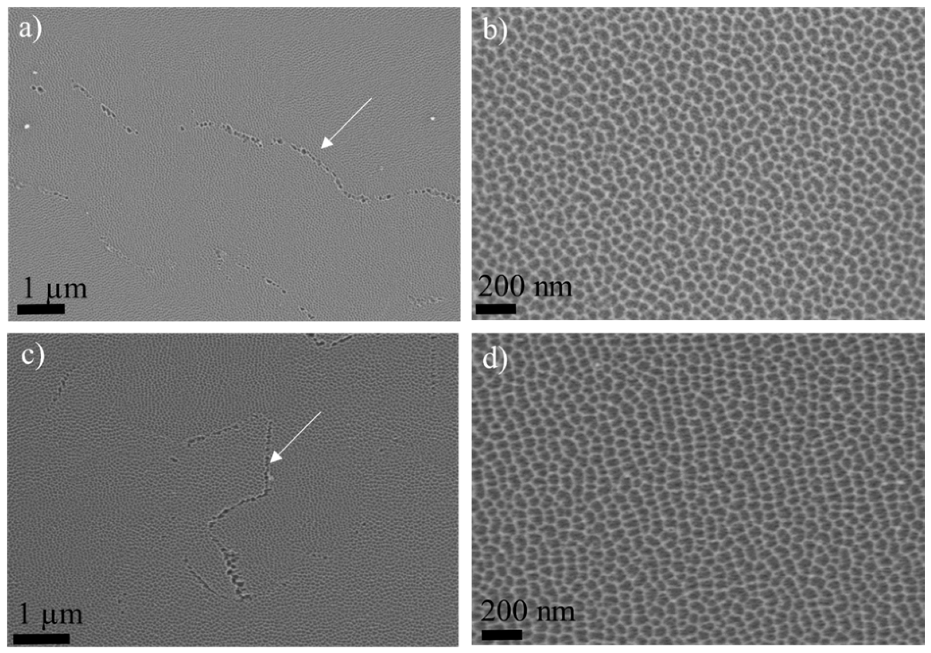
Figure 4 shows the top-view of surface scanning electron micrographs of the specimen surfaces formed in CR18 (CrRef), and after anodising for 300 s, the longest experimental time.
Both surfaces reveal irregularly ordered cells of various sizes and shapes. The cell diameters are 40–72 nm for CrRef (
Figure 4a,b) and 58–65 nm for the Cr300 sample (
Figure 4c,d), corresponding to ratios of 2.4–2.62 and 2.1–2.5 nm/V, in the range of the values obtained for porous alumina, namely, 2.0–2.5 nm/V [
4,
16]. The surface also reveals small clusters of larger pores of diameters from 65 to 150 nm. They probably follow the large grain boundaries of the Al substrate or any other discontinuity of the sample’s surface, such as scratches not removed during electropolishing.
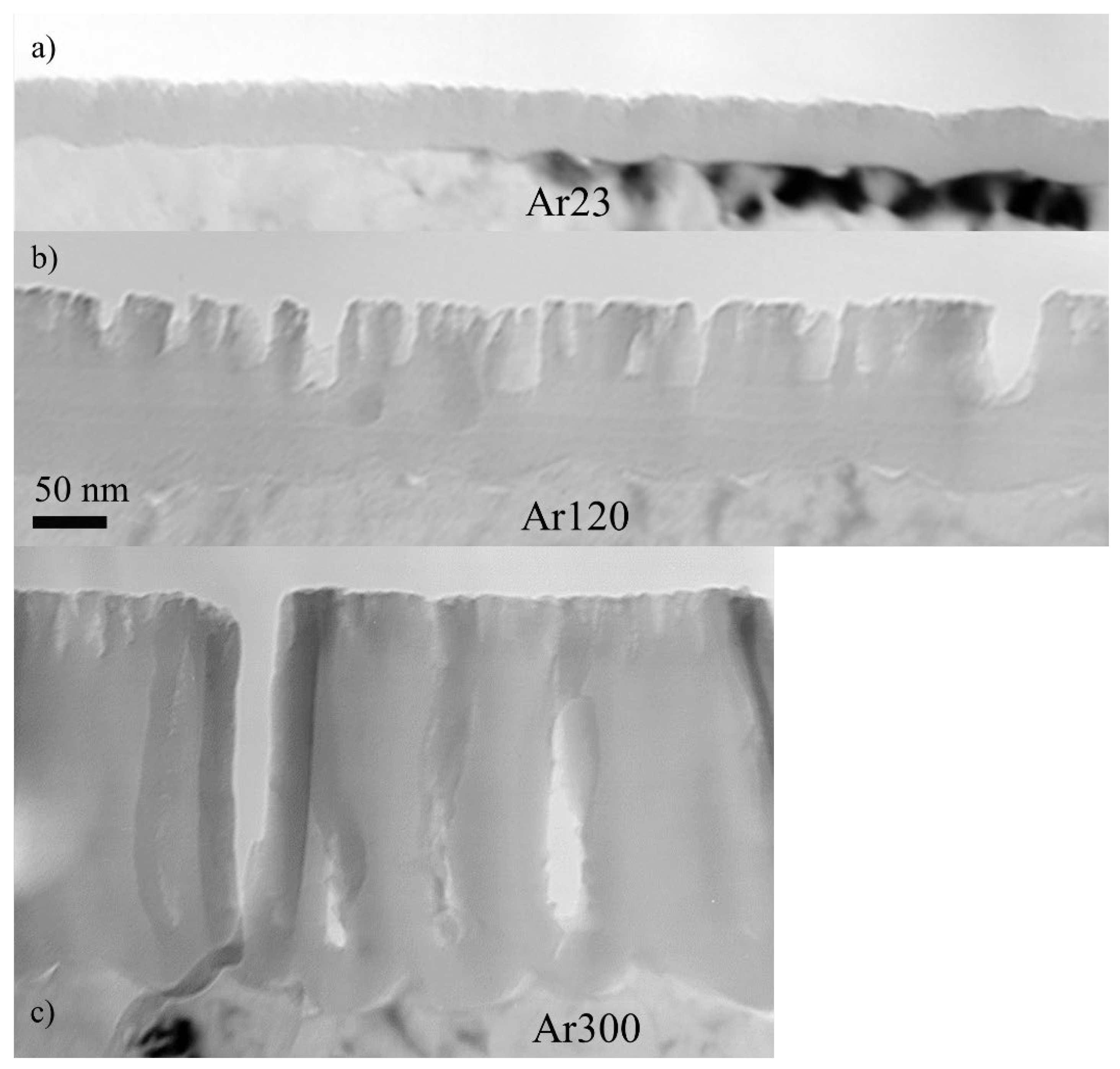
Figure 5 shows transmission electron micrographs of ultramicrotomed cross-sections of specimens formed in AR18 and re-anodized in CR16 for 23 s to reach a voltage of 30 V (Ar23), for 120 s (sample Ar120) and 300 s (sample Ar300). The ArRef sample film thickness is about 25 nm, which indicates a formation ratio of ~1.25 nm/s, the same value reported in [
20]. The anodic films of samples re-anodised in CR16 consist of a barrier region and a porous region, with average total thicknesses of 50, 142, and 315 nm, and the barrier region thickness increases gradually from 25 nm (ArRef) to 35 nm (Ar23) and 65 nm (Ar120), then drops to 43 nm (Ar300).
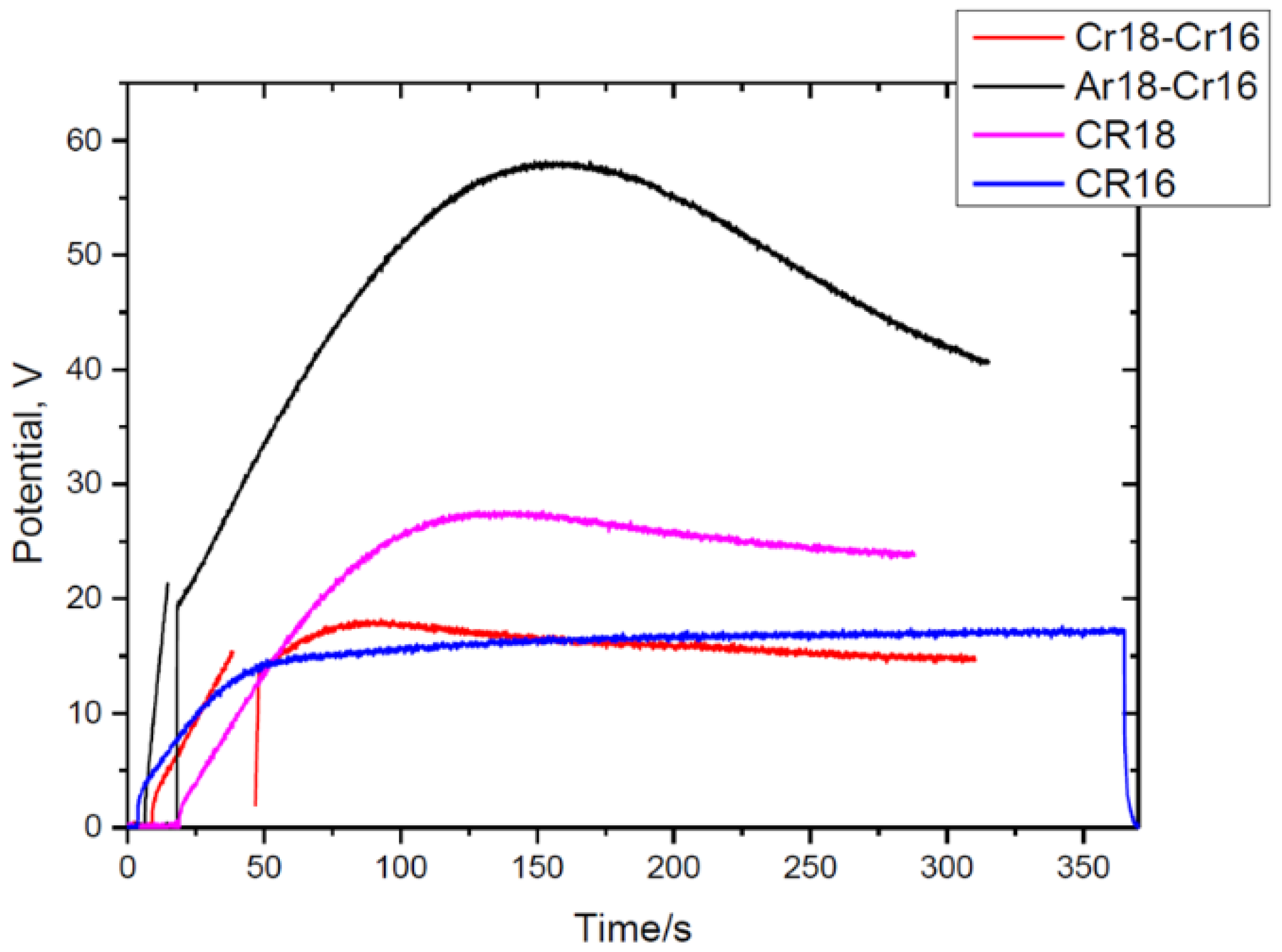
The decrease in the barrier layer thickness is reflected in the reduction in the potential from 58 to 41 V (
Figure 2). The TEM micrographs of the Ar18–Cr16 experiment show similarities to the Cr18–Cr16 experiment in the morphology of the major pores (feather-like type) and the presence of fine incipient pores observed earlier.
The growth rate of the anodic film is 1.08 nm/s for Ar23 and 1.00 nm/s for other samples, and this agrees with the calculated thickness of Al oxidised from the charge passed through the cell. The charges passed in the cell during re-anodising can oxidise 24 nm (Ar23), 121 nm (Ar120), and 301 nm (Ar300) of Al. The volume expansion factors are 1.07, 0.96 ± 0.14, and 0.97 ± 0.065. The average value of the expansion factor (1.00 ± 0.07) is 4% lower than for the previously discussed Cr18–Cr16 experiment (
Table 1).
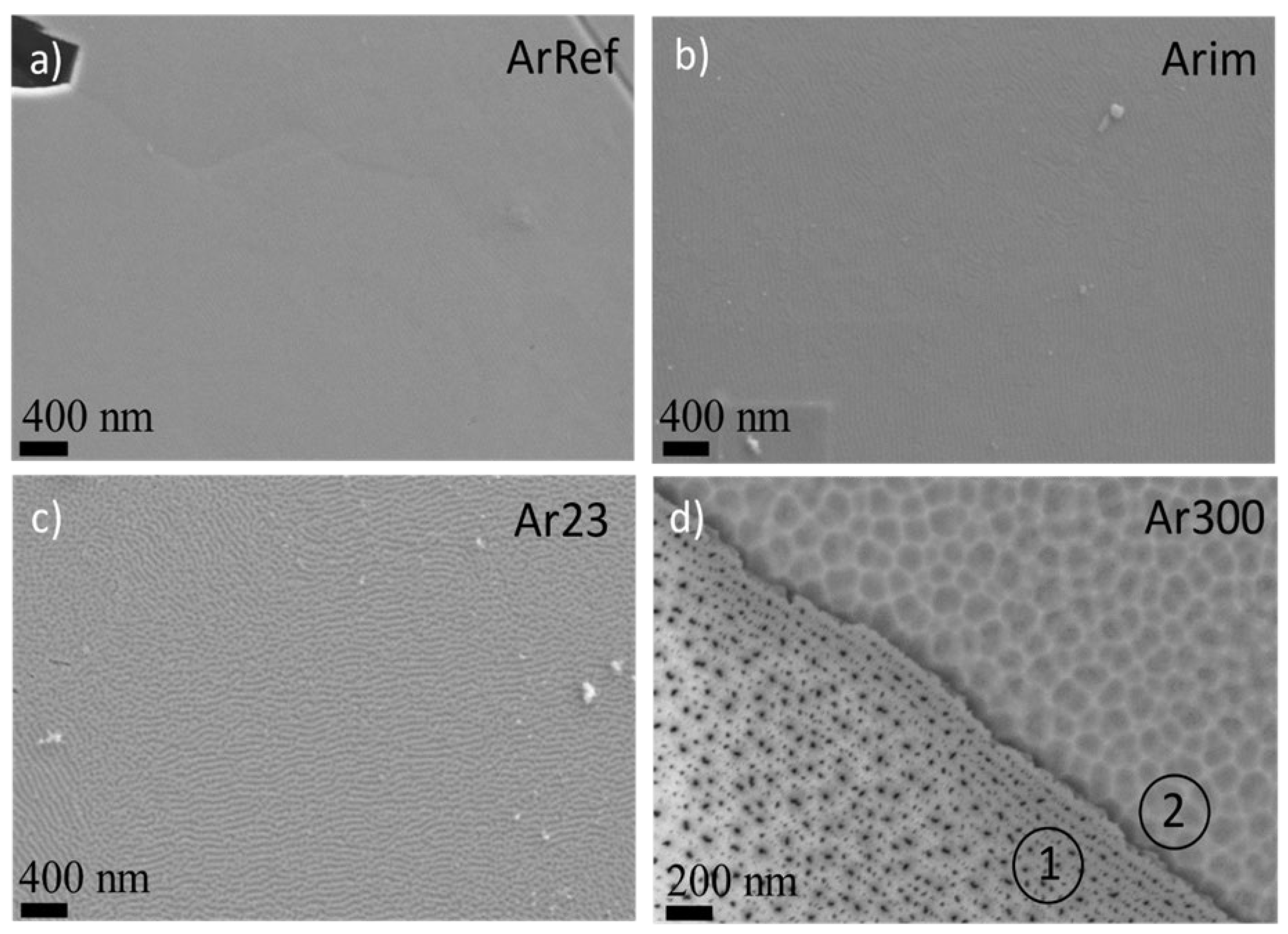
Figure 6 shows scanning electron micrographs of the surfaces of the specimens formed in sodium arsenate (AsRef) and after immersion in chromic acid (Arim) for 300 s; both surfaces reveal regular trenches, inherited from the electropolished substrate due to local differences in the electropolishing rate, and the surface after immersion in CR16 reveals more pronounced ridges. As will be shown later from the surface composition analysis, the immersion removed less than 2 nm of the oxide outer layer containing arsenate species and probably 1–2 nm in addition of the hydrated Al that contained As species. The CR16 at 313 K probably etched some areas of less dense barrier oxide preferentially, this could explain the less uniform-looking surface. Following re-anodising up to 30 V (Ar23) and for another 300 s (Ar300), the undulations of the film seen in cross-section are more pronounced (
Figure 5b,c) and the surface reveals larger pores scattered relatively uniformly over the area (
Figure 6c,d—the surface area indicated by 1). The cell diameter is 150 nm for Ar120 and 100–140 nm for the Ar300 sample. The cell diameter of Ar300 was calculated from the cross-section (
Figure 5c) and from the surface (
Figure 6d,), from which the oxide layer was removed by etching—part of the sample indicated by 2 in
Figure 6d. A part of the sample indicated by 1 contains oxide film in
Figure 6d.
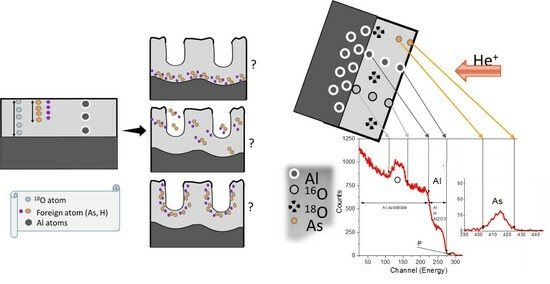
3.5. Re-Anodising in Chromic Acid—Chemical Composition of Film from NRA and RBS
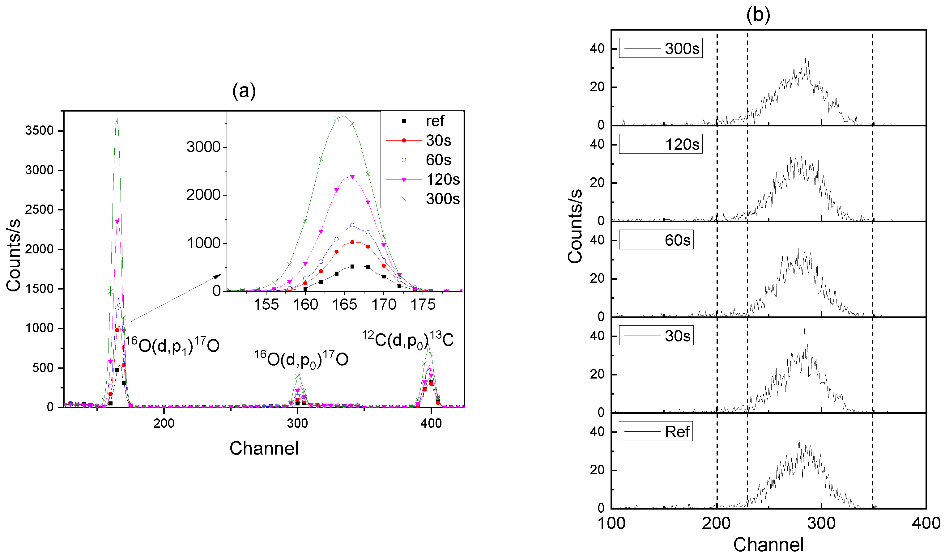
Representative spectra of the
16O(d,p
1)
17O nuclear reaction, which was used to determine the
16O contents of the films, are shown in
Figure 7a. The spectra reveal a small peak for the
12C(d,p
0)
13C reaction, which increases with the increase in the film thickness, probably owing to the greater area of pore surfaces that are available for adsorption of hydrocarbons.
The
18O content of the films was measured using the
18O(p,α)
15N reaction, with the relevant data shown in
Figure 7b. The observed
18O peak position does not change with increasing anodizing time, indicating that the
18O is retained at the alumina–electrolyte interface in the case of the Cr18–Cr16 experiment, in contrast to the Ar18–Cr16 experiment. The
18O in the films originates from the AR18 and CR18 electrolytes (abundance of 10%) and from the CR16 electrolyte (abundance of 0.2%). The
18O from CR16 was estimated as 0.2% of the added
16O and was subtracted from the raw values of
18O. Similarly, the quantity of oxygen (
16O) of 19 × 10
15 atoms/cm
2 measured on electropolished aluminium was subtracted from the oxygen content of the anodised specimens to determine the oxygen added solely by the anodizing process. The accuracy of the values is within ~3%. The summary of the NRA results for the
16O and
18O analyses of the Cr18–Cr16 experiment, oxygen increment from re-anodising, charge passed during re-anodising, Al consumed (from Faraday’s law), and calculated efficiency are provided in
Table 2. The same parameters and, additionally, the percentage of As species loss for the Ar18–Cr16 experiment are provided in
Table 3. The average
18O content of the specimens was 12.52 ± 4 × 10
15 atoms/cm
2, which is 8.21 ± 0.2 at.% of the total oxygen for CR18, and 11.18 ± 1 × 10
15 atoms/cm
2, which is 8.9 ± 0.26 at.% of the total oxygen for AR18. The average
18O enrichment being below 10% in the reference sample ArRef can be explained by the incorporation of As species, since the arsenate ions and water of hydration of the sodium arsenate can reduce the
18O in the films by up to 1% below that of the enriched water.
However, the
18O enrichment is below the expected values for CR18. The anodic alumina formed in chromic acid is considered relatively pure and, in principle, does not contain other foreign species like chromates, contrary to, for example, alumina formed in phosphoric acid. The enrichment reported for phosphoric acid was in the range of 8.8–9.0 at.%, which is slightly below the enrichment of the water, due mainly to the presence of phosphate ions in the films [
17,
20]. Following the re-anodising of CrRef, the
18O content was analysed. The amount of
18O detected in the Cr30 film had not changed compared to the CrRef, which indicates that no
18O was lost within the measurement error in the first 30 s of re-anodising, where we normally would expect electric-field-enhanced dissolution of the alumina. The possible explanation of this observation is provided later where the NRDP measurements are discussed. Then, for Cr60 and Cr120 approximately 4.5% of the
18O is lost, so that later, the loss of
18O is reduced to only 2.5% for Cr300. Immersion of the CrRef sample in the chromic acid at 313 K for 300 s (equivalent period of the longest time of re-anodising) resulted in a loss of 7.22% of
18O. This is equal to a loss of 2–3 nm of alumina due to chemical dissolution.
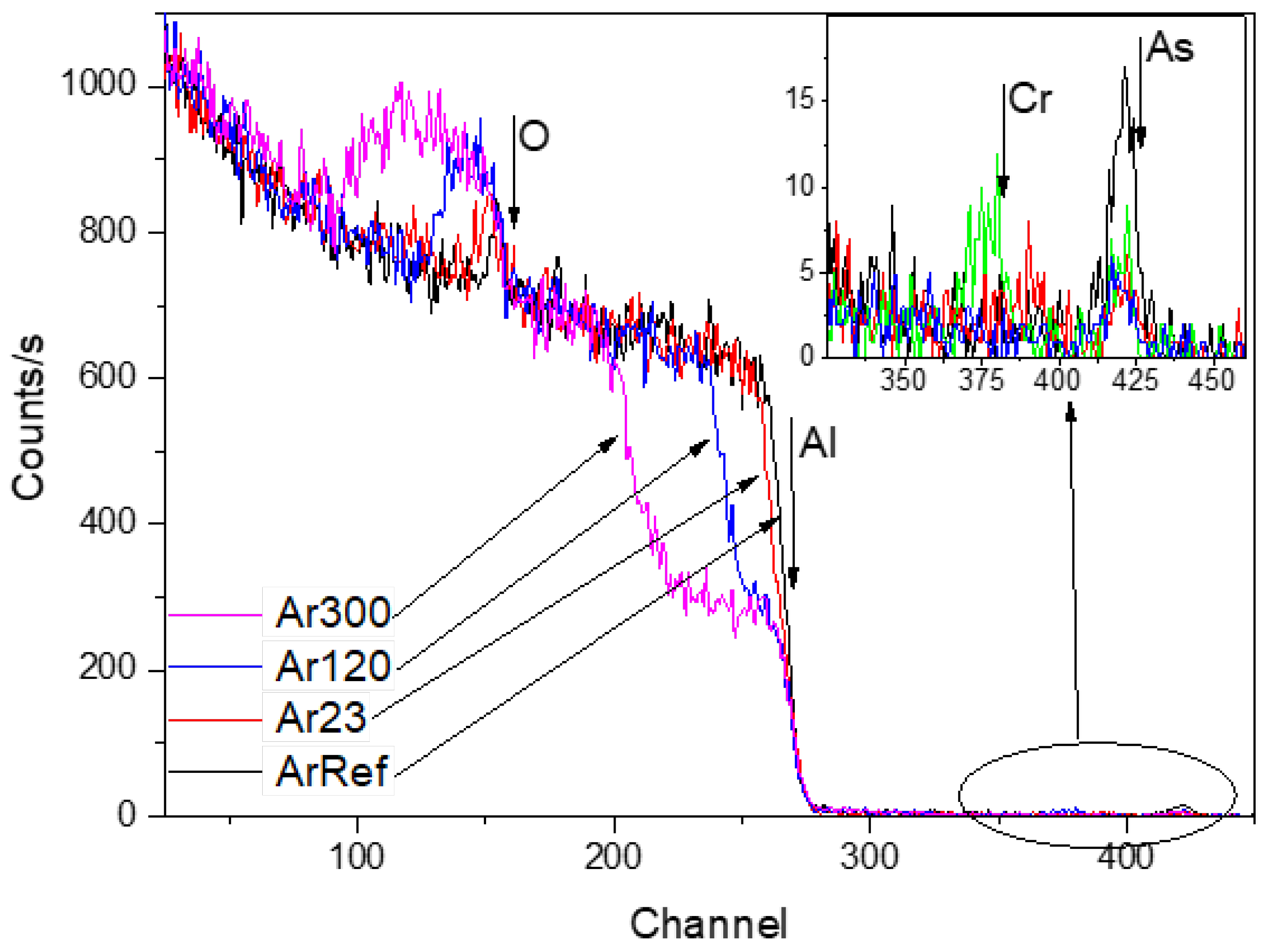
RBS spectra for ArRef, Ar23, Ar120, and Ar300 are shown in
Figure 8. The films formed in arsenate electrolyte are 25 nm thick, with arsenic contained in the outer ~40% to 43% of the film thickness based on TEM and RBS.
The RBS spectra show reduced arsenic peaks following the immersion (not shown here) and re-anodizing treatments. Immersion for 300 s in the chromic acid led to losses of ~0.5% of oxygen and ~37% of arsenic, which is equal to around 3.7 nm of the film. The arsenate peak widths and location were not altered after re-anodizing, which suggests that arsenic was located near the film surface. The spectra reveal yields from aluminium which widened when re-anodising caused the oxides to thicken. The widths of the oxygen yield also increased.
Table 3 reveals that re-anodizing up to 30 V and 60 V, and for 300 s (
Figure 2), led to ~67%, 68%, and 71% losses of arsenic (to an accuracy of ±5%), respectively, which indicates both processes, chemical dissolution and field-assisted dissolution, are responsible for the loss of As from the outer part of the layer of the anodic film. The arsenic species are immobile markers and are likely to be ejected at the start of re-anodising when the outward-migrating Al
3+ ions are ejected to the electrolyte and the pore development is initiated due to field-assisted ejection. The additional 30–34% loss of As due to re-anodising is in relatively good agreement with the 38–43% porosity of the re-anodised samples calculated from the pore-filling experiment, not presented here. Chromium was only detected in one sample, Ar60V, which indicated an atomic ratio of Cr:Al of <0.001 (
Figure 8; Cr and As indicated by arrow in the inception). The absence of a significant chromium content agrees with previous works [
25,
26,
37,
38]. The
18O concentration was also reduced by 4.8%, 7.4%, and 6.1% compared to the original concentrations, to an accuracy of ±3%, in Ar23, Ar120, and Ar300, respectively. The loss of the mobile inward
18O tracers might be interdependent phenomena due to (i) over time, the chemical dissolution of the surface of the pore walls in contact with the electrolyte; (ii) migration of oxygen ions inwards within the barrier alumina under the experimental value of the electric field being slower than the theoretical transport number of 0.6; and (iii) the presence of the space charge [
39] distribution in the oxide film, which has a dual effect. First, it retards the ejection of Al
3+ ions, and second, it prevents O
2− ions from migrating inward.
3.6. 18O Species Distribution Profile in Films
The oxygen isotope
18O is a stable isotope that was proposed for use in ion beam accelerator-based studies of the growth of a barrier anodic layer on tantalum in the pioneering work of G. Amsel and D. Samuel [
33]. The discovery of narrow resonances in the
18O(p,α)
15N nuclear reaction was immediately utilised in the field of stable isotopic tracing of atomic transport processes during thin-film growth, and the
18O (p,α)
15N at 151 keV was used as a probe to analyse the
18O distribution within oxide layers with potentially monolayer precision (NRDP). Subsequently, the French and Hungarian research groups applied the use of the
18O isotope and NRDP to study porous silicon oxides. Later, the NRDP was again resurrected to study the growth mechanism of porous anodic oxides on metals [
11,
17,
19,
20,
22]. In our current work, we could not achieve monolayer precision due to the feather-like porosity of the formed samples and low concentration of 10% of
18O in the electrolyte (due to the high cost of
18O highly enriched water). Both these factors increased the experimental error. Nevertheless, nanometric precision could be achieved through a multi-technique approach, combining NRA, RBS, and TEM with NRDP.
For the NRDP experiment, two additional experimental conditions were applied to the samples described earlier in the experimental section, namely, Cr7–15 and the sample anodised to 7 V in CR18 (Cr7) and re-anodised to 15 V in CR16 (Cr15) at a constant current of 3 mA/cm2. The pre-formed film was a 12–14 nm thick barrier-type film (experiment name: Cr7–15). Two steps anodizing at a constant current of 3 mA/cm2 with the order of the anodizing sequence inverted: the first step in CR16, and second step in CR18 (experiment name: Cr16–Cr18). The results of three samples, Cr60-inv, Cr120-inv, and Cr300-inv, were analysed, which are the equivalent of Cr60, Cr120, and Cr300 presented earlier.
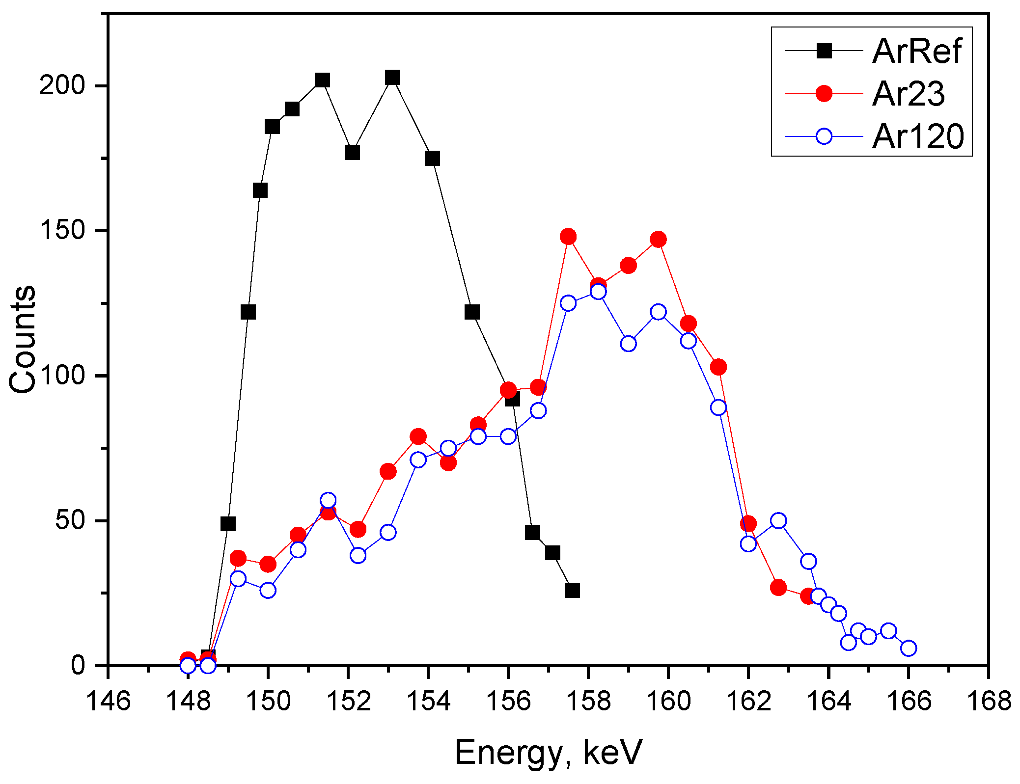
The results of nuclear resonance
18O depth profiling for aluminium following anodizing to 7 V at 3 mA/cm
2 in CR18 at 313 K (sample Cr7) and re-anodizing to 15 V in CR16 (sample Cr15) are shown in
Figure 9a. The raw data were recorded as energy vs. counts. For better clarity, these data were converted to thickness (nm) and concentration (%), assuming that the reference sample for every experiment initially had 100%
18O tracer in the film. The experimentally calculated stopping power of ions in alumina was used to convert energy from keV units to thickness in nm units. The ratio of the width at half-maximum of the excitation curve and the path length of the beam in the film with a density of 3.1 g/cm
3 indicated a stopping power of 0.25 keV/nm, which was used for fitting all of the present data using the SPACES software [
40]. In comparison, a stopping power of 0.149 keV/nm was obtained for 151 keV protons from SRIM in a film with a density of 3.1 g/cm
3 formed in phosphoric acid, containing units of Al
2O
3 and AlPO
4 with a P:Al atomic ratio of 0.05 [
19,
20,
41].
The thickness of the barrier film in Cr7 is 12.2 nm and the
18O distribution is uniform based on NRDP. However, the starting edge of the increased
18O concentration in the Cr7 sample is shifted to a higher energy of 151.6 keV compared to sample Cr15, for which the resonance energy is almost exactly at 151 keV at the sample surface (indicated by the arrows). This may suggest that the
18O is buried under the 2 nm oxide layer of normal
16O abundance, shown schematically in
Figure 9a. The voltage at the commencement of the anodizing process jumps to 2.4 V. Assuming that the natural oxide film is 2–3 nm thick, it indicates that the electric field (Ef) across the natural oxide layer is 8–10 MV/cm. The Ef of 8 MV/cm probably facilitates
18O migration through the natural barrier layer and formation of the new oxide at the film–metal interface and at the same time prevents a dissolution of the natural oxide film. According to the authors of [
42], the presence of gel layers during anodizing of high-purity aluminium in molybdate or tungstate electrolytes promotes the formation of alumina by reducing the field-assisted ejection of Al ion. Thus, a similar phenomenon may occur in arsenate, preserving the native oxide layer. Within the first 15 s of anodising, the Ef decreases from 8 to 5.6 MeV/cm due to the added oxide thickness. The calculated growth efficiency of the oxide layer is approximately 22%. This may suggest that the current is consumed on other (parasitic) processes instead of oxidising the Al substrate. Following the re-anodising in CR16, the leading edge of the
18O nuclear reaction resonance shifts to 151 keV (
Figure 9a, indicated by arrow). This may be due to the dissolution of the outer 2 nm natural oxide film by chemical dissolution, thus exposing the
18O present beneath. The Cr15 sample film thickness increases to 30 nm, and it consists of a 13.5–15 nm thick barrier layer and a 16.5–18 nm porous outer part (
Figure 3a and
Figure 9a). The efficiency slightly increases to 25%. The NRA indicates no measurable loss of
18O after re-anodising up to 15 V, with 75–80% of the
18O distributed in the porous part and the remaining 20–25% in the barrier layer. The above findings regarding the burial of the
18O beneath the natural oxide layer during the initial period of anodising can explain why no measurable amount of
18O was lost from the Cr15 and Cr30 samples. On the other hand, the immersion of the CrRef for 300 s results in a loss of approximately 7% of the
18O due to chemical dissolution. It may be suggested that the combination of the presence of gel at the top of the oxides and the electric field at the part below, measuring 8 MeV, is sufficient to prevent dissolution of the oxide.
Moving on to discuss the Cr18–Cr16 experiment, the NRDP
18O profiles of the consecutively anodised samples Cr30, Cr60, Cr120, and Cr300 look identical. The majority of the tracer is located in the outer surface (
Figure 9b). Additionally, the NRDP profile is shown for the sample anodized solely in
18O for a prolonged time. It should be noticed that NRDP is useful only to a certain thickness of the films. The results obtained from thicker samples, in the case of the porous alumina films above 100 nm, are affected by phenomena relating to the interaction of a probing beam of ions with solid matter (i.e., multiple scattering). These interactions can render the interpretation of the results ambiguous or less reliable. Thus, we limited the interpretation to CrRef, Cr7, Cr15, and Cr30 (
Figure 9a and
Figure 10), and the NRDP profile obtained for Cr30 and its reference CrRef (
Figure 10).
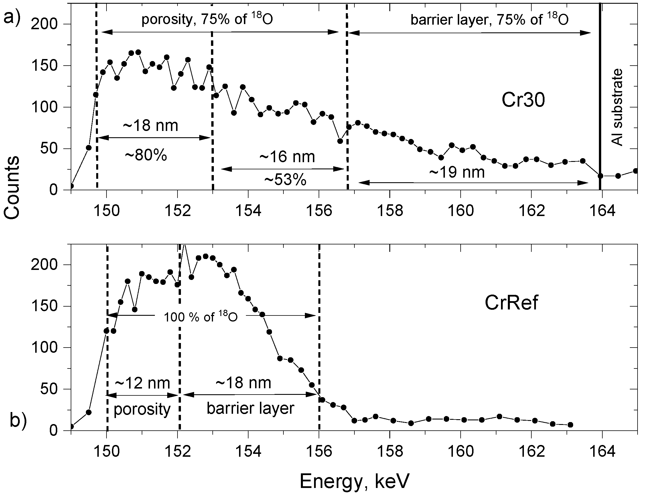
The
18O tracer is distributed uniformly within a thickness of the reference sample CrRef. Two parts of the profile can be distinguished. The 12.5 nm thick outer part shows an apparently lower
18O concentration, and the part next to the metal is an 18 nm thick region. This corresponds well with the cross-sections of the film which consist of a 19 ± 2 nm barrier layer and a 12 ± 2 nm porous outer region. The apparent drop in the tracer concentration in the spectrum of CrRef is a consequence of the porosity: the probability of the p-α reaction with the
18O tracer is reduced due to a lower amount of material available for the interaction. The interpretation of the apparently reduced tracer concentration at energies of approximately 154.5–156 keV is not straightforward. One explanation might be that the chemical composition of this part of the film, approximately 3 nm thick, adjusted to the metal, is not pure alumina of a stoichiometric Al:O ratio, with Al ions in a higher concentration than expected. This trend, however, was observed for a SiO
2 reference sample enriched to 90% of
18O (complementary data available upon request); thus, it is assumed that the cause is linked to a systematic error related most likely to the resolution of the measurement due to beam widening and the specific geometry of the experiment. Following re-anodizing for 30 s, the tracer profile widens following the increase in the thickness of the growing film (
Figure 10). Three regions can be distinguished: an 18 nm thick outer region with the concentration reduced by a further 20% compared to CrRef; a 16 nm thick inner region, where the tracer concentration is reduced by 50%; and a 17.7–19 nm inner region with the tracer concentration gradually reducing to zero. To conclude the results of the Cr18–Cr16 experiment, it is quite clear that re-anodizing conditions do not enhance the movement of
18O within the oxide layer, and that there is no significant widening of the
18O signal. Thus, it is apparent that the tracer stays in the outer part of the growing porous oxide film.
Moving on to the Ar18–Cr16 experiment,
Figure 11 presents the profiles obtained for ArRef (barrier-type film), Ar30 (initiation of fine porosity), and Ar120 (establishing of main pores). The
18O tracer distribution is different to the earlier discussed experiment and resembles the behaviour of tracers observed during re-anodising in phosphoric acid [
17,
20]. The Ef increases during anodizing: 8.0 MV/cm (ArRef), 8.6 MV/cm (Ar23), 9.25 MV/cm (Ar120), and 9.3 MV/cm (Ar300). The anodizing efficiency is 43% for Ar23, and reaches a constant value of 47% for the rest of the anodizing time.
The decoupling of the kinetic and morphological interaction between the metal–oxide and oxide–electrolyte interfaces during anodizing is not a trivial task [
43]. From our results, it seems that the higher Ef facilitates
18O migration inwards ahead of advancing pores towards the oxide–metal interface, similar to the behaviour observed in phosphoric acid. However, the higher electric field does not increase the calculated efficiency of the process, which is comparable for both experiments. In phosphoric acid under potentiostatic anodization conditions, the observed film growth efficiency is around 60–70%, even at the low currents observed (less than 2 mA/cm
2), as long as the applied voltage is large (110 V). This indicates that Al ions undergo field-assisted ejection to the electrolyte at the bottom of the pores and the oxide is formed at the oxide–metal interface due to O ion migration. This would suggest that the inward migration of ions plays a crucial role, like phosphorus, in the increasing efficiency of the porous film growth, thanks to the increased plasticity of the alumina and flow of the material.
The observed differences in
18O transport between the Cr18–Cr16 and Ar18–Cr16 experiments might be attributed to the presence of As in the initial layer, its varying densities, hydrogenation, or the presence of trapped electrons and magnetic domains [
44]. According to the work of J. Lambert and I. Vrublevsky, negative charges are located in the subsurface region of the barrier-type alumina outer layer. They also concluded that a larger accumulated negative charge results in a higher rate of anodic oxide growth. These negative charges are likely electrons trapped by structural defects created by mechanical stress induced by the incorporation of impurities during film growth [
8,
38,
45], as well as the ionisation of water molecules, yielding electrons, protons, and gaseous oxygen [
46].
In our experiment, although the re-anodizing conditions are the same (constant current of 3 mA/cm2), the effect of the initial conditions of the pre-formed layer seems to dictate to some extent the porosity formation during the later stage of anodizing. The two experiments’ starting points are different: a barrier layer containing foreign ions (Ar18–Cr16) and a pure alumina film with embryo pores (Cr18–Cr16). The first step in anodizing of the Cr18–Cr16 experiment was carried out at a 3 mA/cm2 current density, whereas Ar18–Cr16 was carried out at 5 mA/cm2. After initiation of the pore growth, the barrier layer for Cr18–Cr16 (also for the Cr7–15 experiments) does not increase significantly and reaches a constant value for all samples ~23 nm and ~13 nm.
On the other hand, in the Ar18–Cr16 experiment, the barrier layer thickness increases up to 60 nm and then decreases and stays at a constant value of approximately 43 nm for the longest anodising time. This corresponds to an electric field (Ef) in the range of 8.5 to 9.2 MeV/cm. In contrast, for the Cr18–Cr16, the Ef never exceeds 8.2 (ranging from 5.8 to 8.2), and at the intermediate stage of anodising the Ef oscillates around 8 MV/cm. For comparison, with the borax and phosphoric acid electrolytes we observed a thinning of 60 nm of the pre-formed barrier-type alumina until a specific Ef was reached, then the steady growth of pores commenced.
The question arises to what extent does the value of the current density during the first stage of anodizing affects the second stage of the anodizing process? It is unclear whether the morphology or electronic conditions of the pre-formed film play a significant role. The additional experiment Cr7–15, where pure barrier-type alumina on the Cr7 sample was pre-formed (in contrast to CrRef of the CR18–CR16 experiment), still shows a location of 18O similar to the results obtained for the Cr18–Cr16 after re-anodising. Therefore, the predominant factor is likely linked to the presence of the embedded charges’ distribution, responsible for ion transport through the film under the electric field, rather than morphological features such as flaws and embryo pores.
Is the presence of trapped negative charges and their distribution across the film related to current density? The DeWitt and Thornton model [
47] predicts that the potentiostatic and galvanostatic anodising yield the same embedded charge density at the same current. In our experiment, the first stage films are formed at 3 mA/cm
2 and 5 mA/cm
2. This difference in current density could be the reason behind the different behaviours of the
18O tracer in the second stage of anodizing. A higher current during formation of the initial film causes conditions in the oxide film to mobilise the
18O later and supports
18O transport away from the incipient pore base under the electric field. If it is agreed that the high accumulation of electrons enhances the film growth, it may be that the 3 mA/cm
2 current density is not high enough to introduce a sufficient number of trapped negative charges to enhance the film growth in the later stage of re-anodizing.
According to previous publications, the plastic flow mechanism of porosity development in alumina is observed when the calculated efficiency is above 60%. The calculated efficiencies for porous film growth in chromic acid are 40–50%, which may indicate that field-assisted ejection is the governing force for pore formation and growth and that flow of the alumina is minimal. Another phenomenon related to doping of the alumina might be responsible for the flow mechanism. It is already well quantified that sulfur anions from sulfuric acid, phosphoric anions from phosphoric acid, or carbon from oxalic acid are incorporated into the few-nanometre-thick outer parts of the pore wall or might be located in almost 100% of the wall material. Skeldon and co-authors demonstrated that a small addition of sulfur ions into the chromic acid may cause noticeable changes in the anodizing process and morphology of the pores and increase the film growth efficiency [
26]. The authors also suggested two possible competing mechanisms: electric-field-assisted dissolution (also called an electric-field-assisted ejection) and field-assisted flow of oxide materials, both of which are difficult to isolate in experimental work [
13]. The same authors [
13] also suggested that anodic film contaminant ions do not affect the porosity initiation and growth. The observed movement of
18O may suggest that the same underlying mechanisms may govern the porosity initiation in chromic acid when the pre-formed barrier layer has specific electronic properties (trapped charges distribution). The presence of As in the form of arsenate ions or As
2O
5 species, with a ratio of As:Al of 0.04 at the outer layer up to 3–4 nm, may have an effect on the charge distribution within a 13–18 nm thick layer. Consequently, the distribution of negative and positive charges might play a role in the initiation of pores through a flow mechanism rather than electric field-assisted ejection. In this context, the marker itself also affects the mechanism of pore initiation. There are indications based on time-of-flight secondary-ion mass spectrometry (ToF-SIMS) analysis that the arsenate distribution within the pre-formed oxide layer might be more complex. Thus, the charge distribution or the permanent polarisation domain may form specific channels when the external electric field is applied. From the preliminary data, it can be seen that in a 25 nm barrier film (ArRef), two regions enriched in As are detected: an outer region (electrolyte/oxide film), approximately 3 nm thick, and a region next to the metal, also about 3–4 nm thick. These results will be the subject of future investigation. These zones must undoubtedly also contain hydrogen, although this fact has not been studied in detail or precisely quantified in the literature. The oxide film formed on an Al–6.5 at.% W alloy during anodising contained ~0.1–0.3 at.% hydrogen, originating from either the electrolyte or the alloy, measured using elastic recoil detection and nuclear reaction analyses [
48]. The application of deuterium in the electrolyte to trace incorporation of hydrogen during anodization will be the subject of further study.


