Article

Influences of Cu Doping on the Microstructure, Optical and Resistance Switching Properties of Zinc OxideThin Films

1
Department of Electrical Engineering, Tunghai University, Taichung 40704, Taiwan
2
Department of Information and Communication Engineering, Chaoyang University of Technology, Taichung 413310, Taiwan
3
Department of Electronic Engineering, Center for Environmental Toxin and Emerging-Contaminant Research, Super Micro Mass Research & Technology Center, Cheng Shiu University, Chengcing Rd., Niaosong District, Kaohsiung 83347, Taiwan
4
Department of Electronic Engineering, Hsiuping University of Science and Technology, Taichung 41280, Taiwan
*
Author to whom correspondence should be addressed.
Nanomaterials 2023, 13(19), 2685; https://doi.org/10.3390/nano13192685
Submission received: 9 August 2023 / Revised: 28 September 2023 / Accepted: 28 September 2023 / Published: 30 September 2023
(This article belongs to the Special Issue Nano-Structured Thin Films: Growth, Characteristics, and Application)

Abstract

:
Copper-doped zinc oxide films (Zn1−xCuxO) (x = 0, 2%, 4%, 6%) were fabricated on conductive substrates using the sol-gel process. The crystal structure, optical and resistive switching properties of Zn1−xCuxO films are studied and discussed. RRAM is made using Zn1−xCuxO as the resistive layer. The results show that the (002) peak intensity and grain size of Zn1−xCuxOfilms increase from 0 to 6%. In addition, PL spectroscopy shows that the oxygen vacancy defect density of Zn1−xCuxO films also increases with the increase in Cu. The improved resistive switching performance of the RRAM device can be attributed to the formation of conductive filaments and the destruction of more oxygen vacancies in the Zn1−xCuxO film. Consequently, the RRAM device exhibits a higher low resistance state to high resistance state ratio and an HRS state of higher resistance value.

1. Introduction

In recent research, resistive random access memory (RRAM) devices have been developed using various binary oxide materials, making them highly attractive for next-generation memory applications due to their fast operation, simple structure, low power consumption, nondestructive readout, long data retention, ease of fabrication, and cost-effectiveness [1,2,3,4,5]. Among the different oxide materials, ZnO-based semiconductor thin films are widely employed in RRAM devices. The ZnO-based semiconductor was investigated for its potential applications in RRAM, due to its low carrier trapping degree, non-toxicity, and simple chemical composition [6,7,8,9,10].Recent studies have indicated that doping zinc oxide with transition metals can effectively reduce its intrinsic carrier density [11,12]. Specifically, La doping has been found to decrease the oxygen vacancy density in ZnO thin films, leading to an improved ON/OFF ratio in RRAM devices [13]. Numerous studies have also demonstrated RRAM characteristics in various doped ZnO thin films [14,15,16,17,18]. Additionally, researchers have explored Cu-doped ZnO materials, the grain size of which can be controlled by the amount of copper doping [19,20]. Cu is considered a suitable dopant for ZnO due to its similar ionic radii to Zn and its ability to act as a deep receptor, binding with adjacent O vacancies in the ZnO lattice [21,22].
We investigate the effects of copper on the electrical, structural, and switched resistive properties of Zn1−xCuxO thin films. The Zn1−xCuxO was synthesized on FTO substrates through the sol-gel process, followed by rapid thermal treatment. The crystallization and microstructure of the samples were analyzed using an X-ray diffractometer and a scanning electron microscope, respectively. RRAM devices employing Zn1−xCuxO thin films were thoroughly examined, and their bipolar switching characteristics were analyzed and discussed.

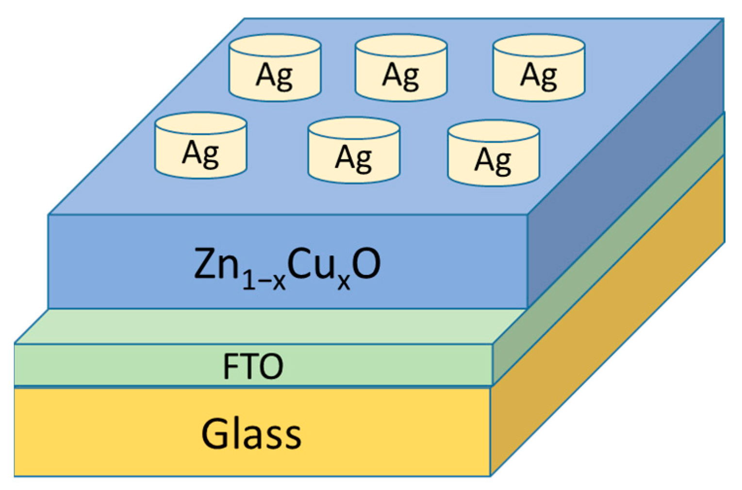
2. Experimental Section

In this research, we prepared thin films of Zn1−xCuxO (x = 0%, 2%, 4%, 6%) using the sol-gel process.Zn1−xCuxO films were prepared using a sol-gel method, employing zinc acetate dihydrate (CH3COO)2Zn·2H2O and copper acetate monohydrate (Cu(CH3COO)2·2H2O) as precursor materials. The precursors were dissolved in 2-Methoxyethanol solvent to maintain a constant metal ion concentration of 0.05 M. Ethanolamine was added to ensure solution stability. These solutions were stirred at 60 °C for three hours using a magnetic stirrer and then allowed to stand for 72 h to obtain transparent solutions. The sol-gel solution was deposited onto a substrate mounted on a spin coater using a two-step spin process. The deposition step began with spinning at 1000 rpm for 10 s and then at 3000 rpm for 30 s. Subsequently, the samples were annealed on a hot plate at 300 °C for 2 min to remove the solvent. The entire process was repeated ten times to achieve the desired film thickness. Finally, the film was annealed at 600 °C for 2 min in a rapid annealing system. The annealing rate was 100 °C/min. The thickness of Zn1−xCuxO film was 500 nm withα-step surface profiler.
Crystallization of samples was analyzed using XRD. To study the optical properties of Zn1−xCuxO, we conducted transmittance optical measurements using a UV spectrometer. The effect of the fluorine-doped tin oxide (FTO) substrate was also taken into account during the transmittance correction. This is due to the fact that FTO substrate can absorb light in the UV-visible range. The transmittance may be measured inaccurately. We used a blank FTO substrate (without Zn1−xCuxO sample) for reference measurements. To correct for substrate effects, the transmittance of the FTO substrate alone was subtracted from the transmittance of the sample and substrate combination. These corrected transmittance data represent the transmittance of the Zn1−xCuxO sample without FTO substrate contribution. For analyzing optical emissions, photoluminescence spectroscopy was employed, covering a wavelength range from 350 nm to 600 nm. In addition, we characterized the switching properties of current-voltage for the Zn1−xCuxO thin films in RRAM. RRAM with a Ag/Zn1−xCuxO/FTO structure was measured using a semiconductor parameter analyzer. Figure 1 shows a schematic diagram of an RRAM device with Ag electrodes. One hundred circular top silver electrodes (100 nm thickness and 0.05 cm diameter) were fabricated on top of the Zn1−xCuxO layer using thermal evaporation technique at 5 × 10⁻⁶ torr.

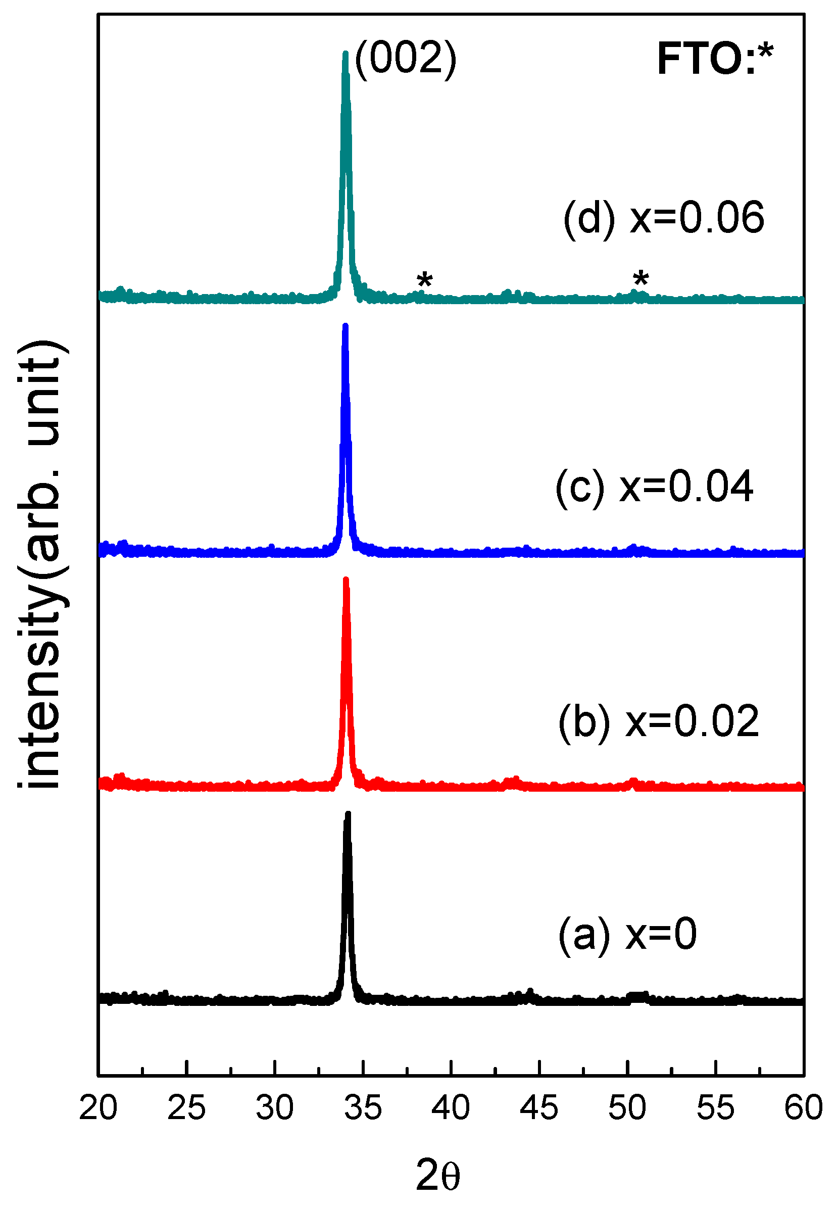
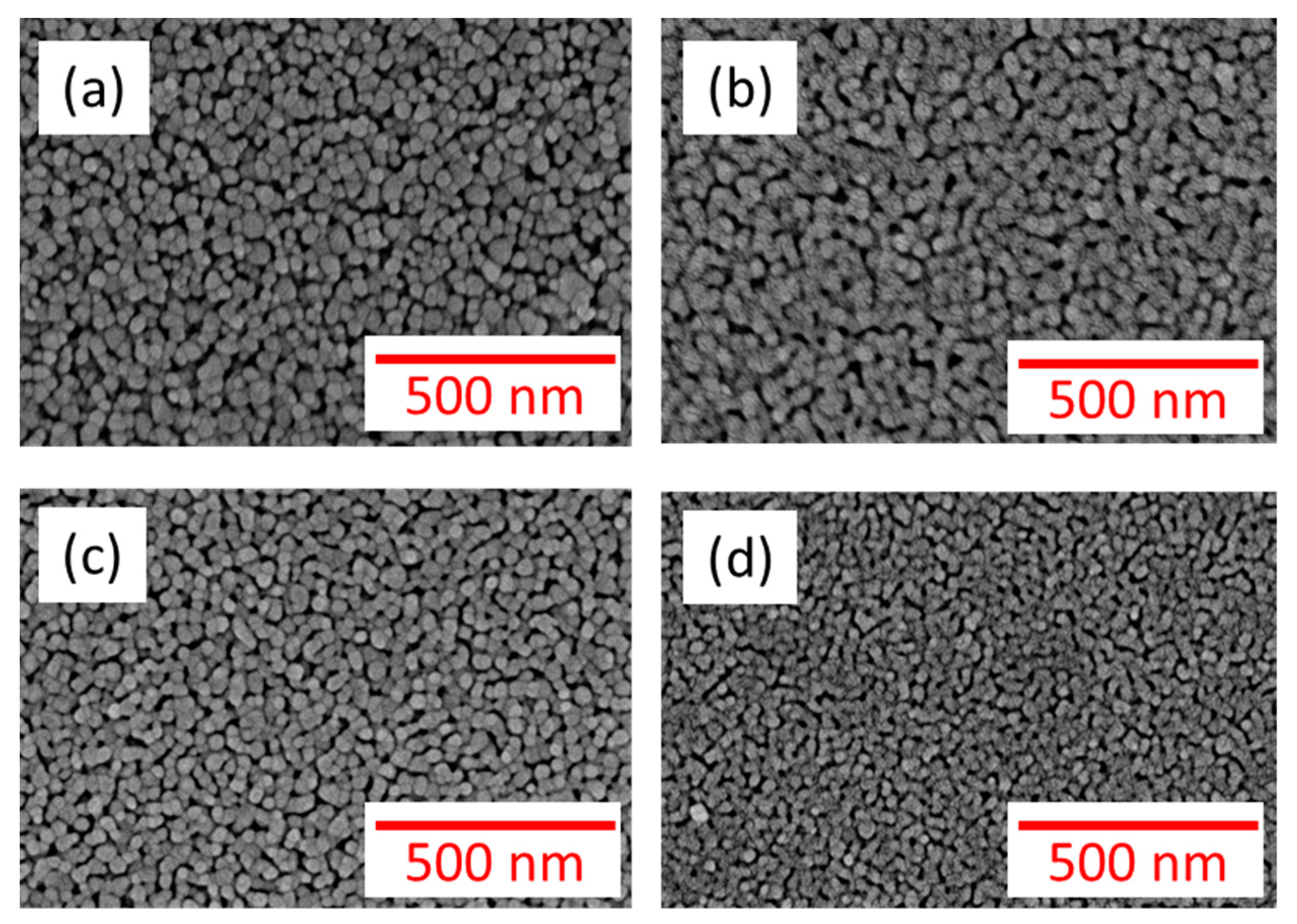
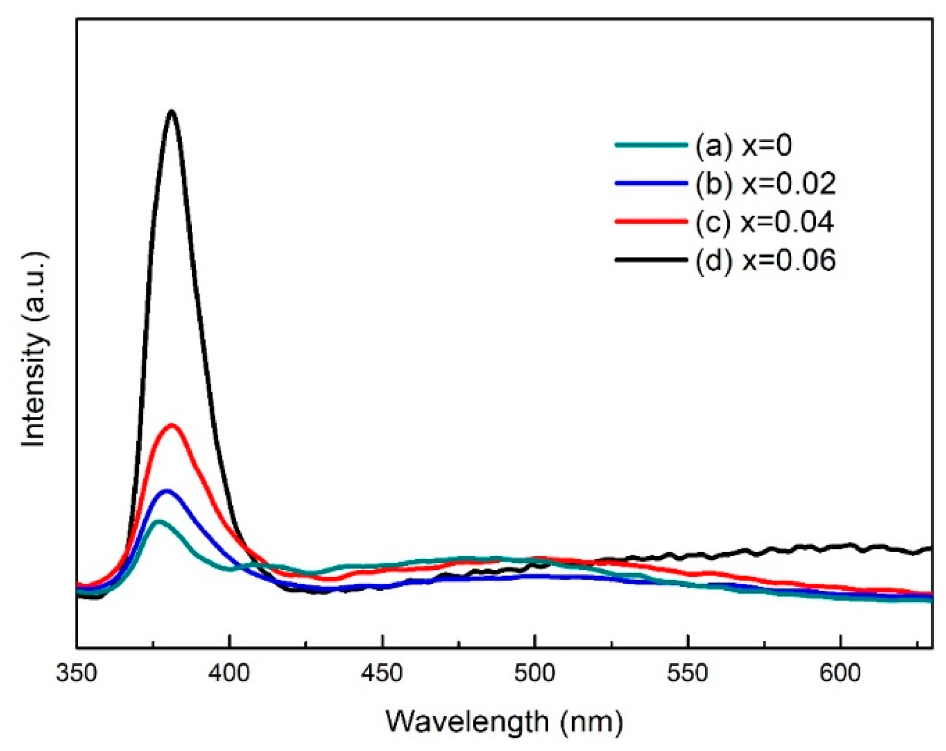
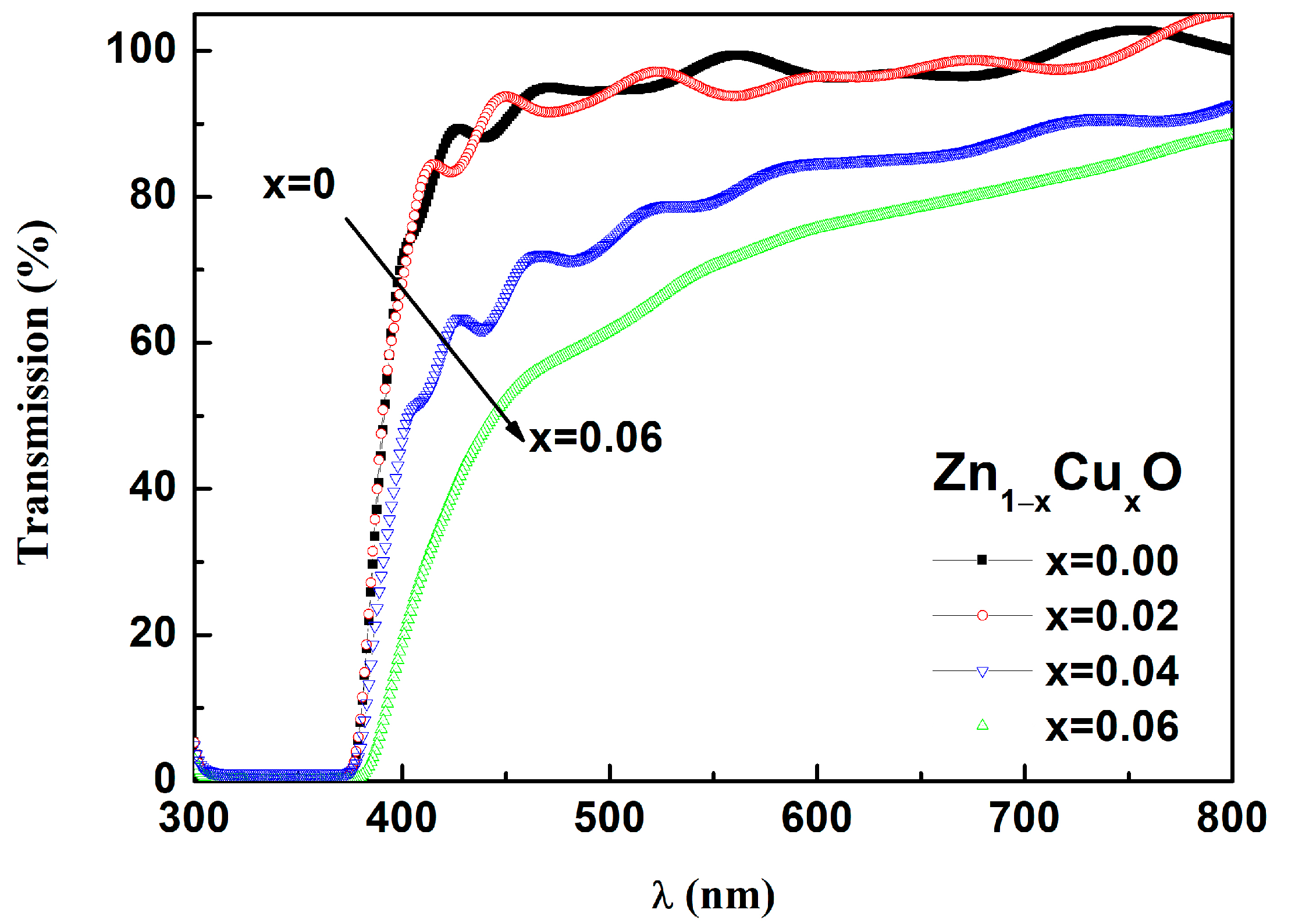
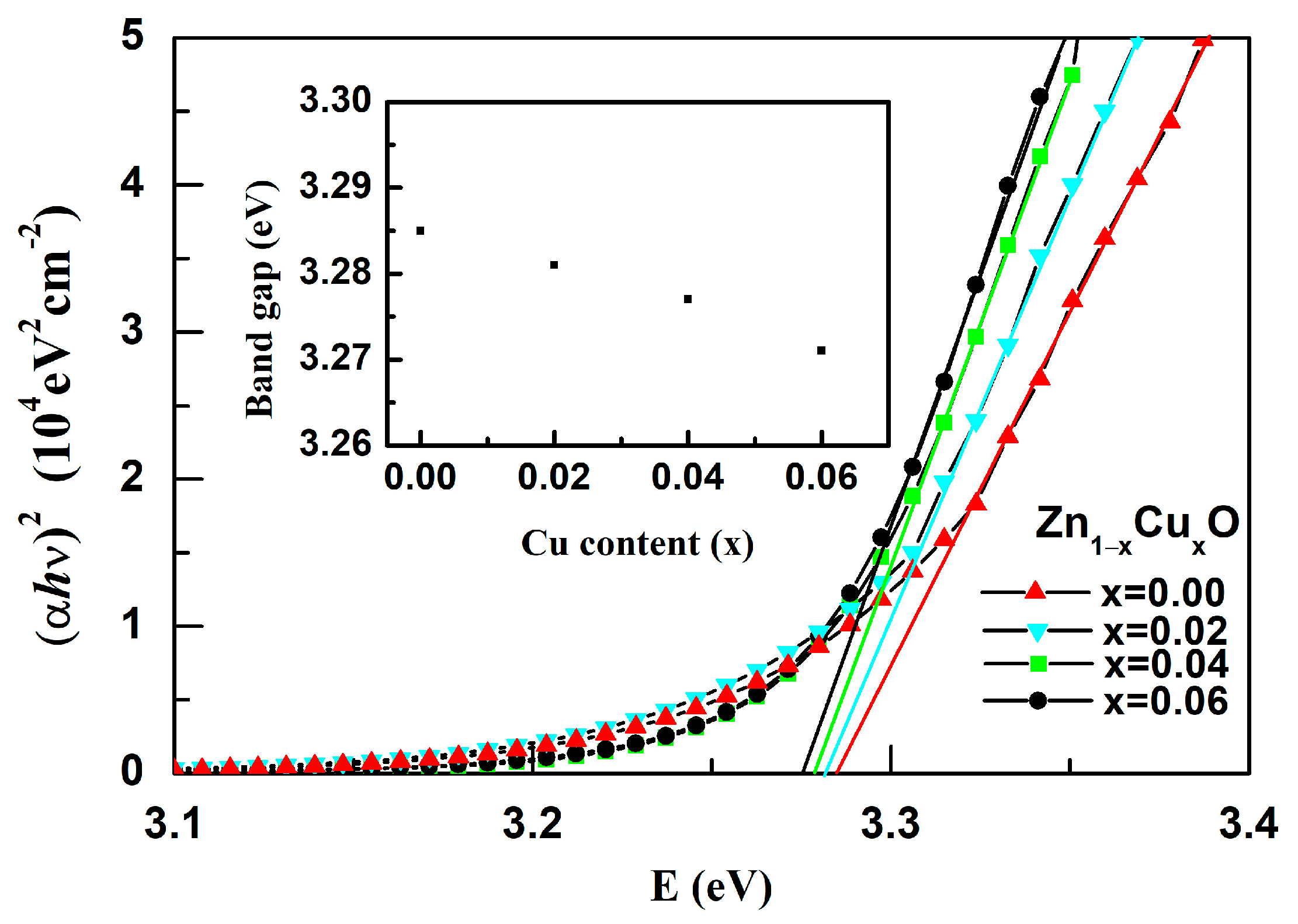
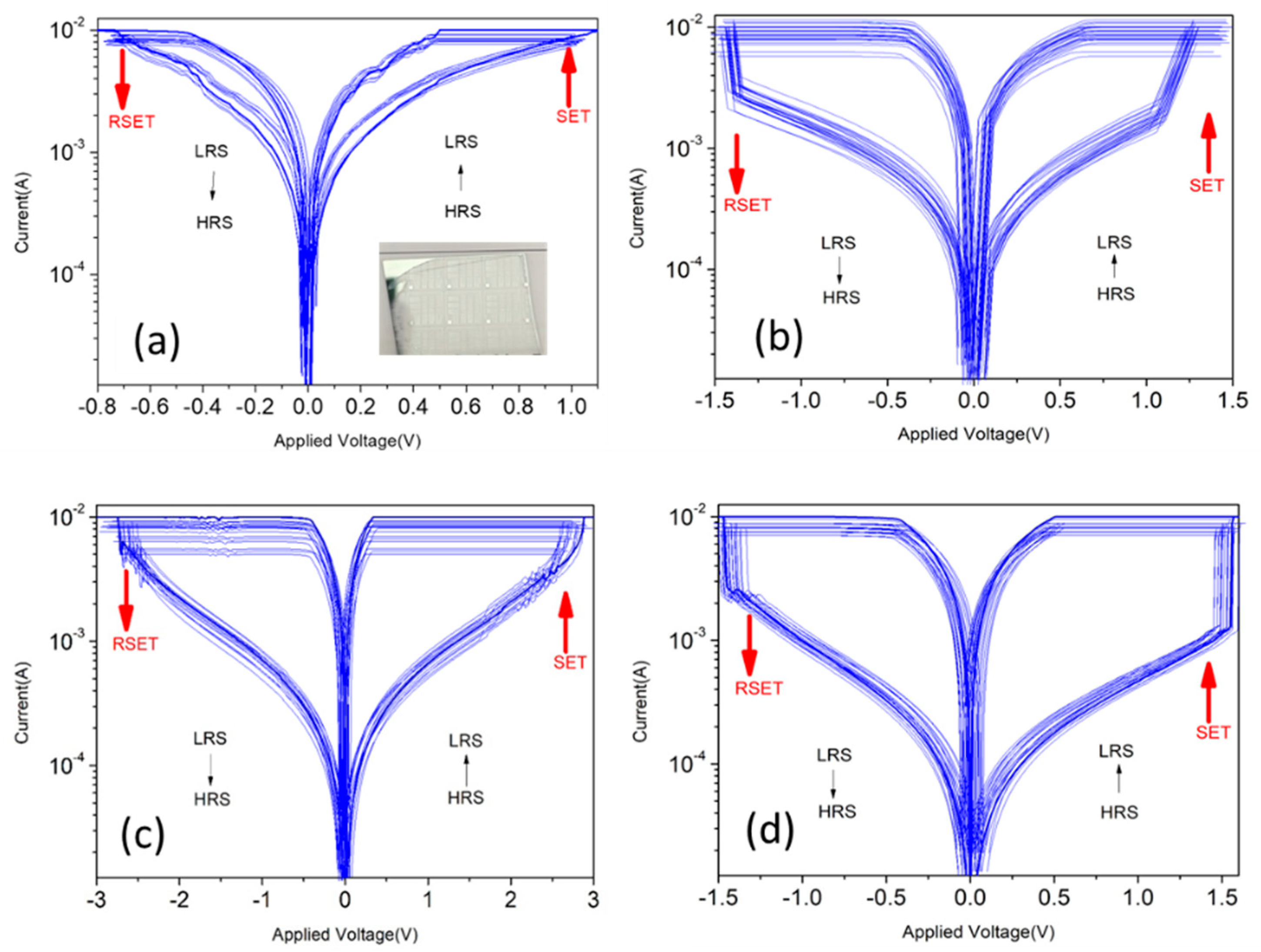
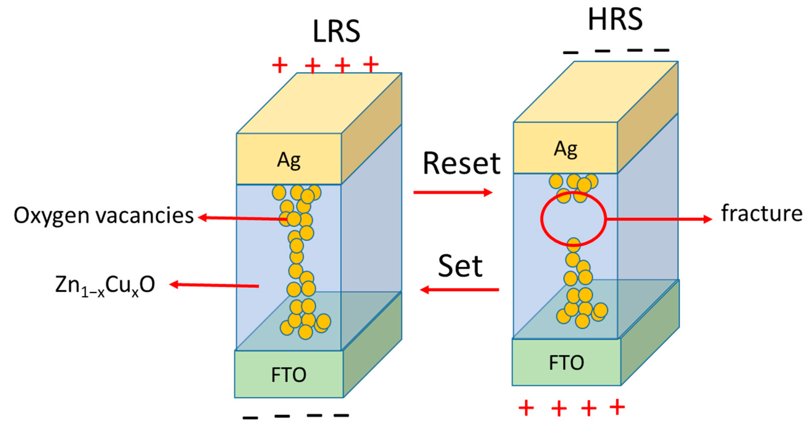
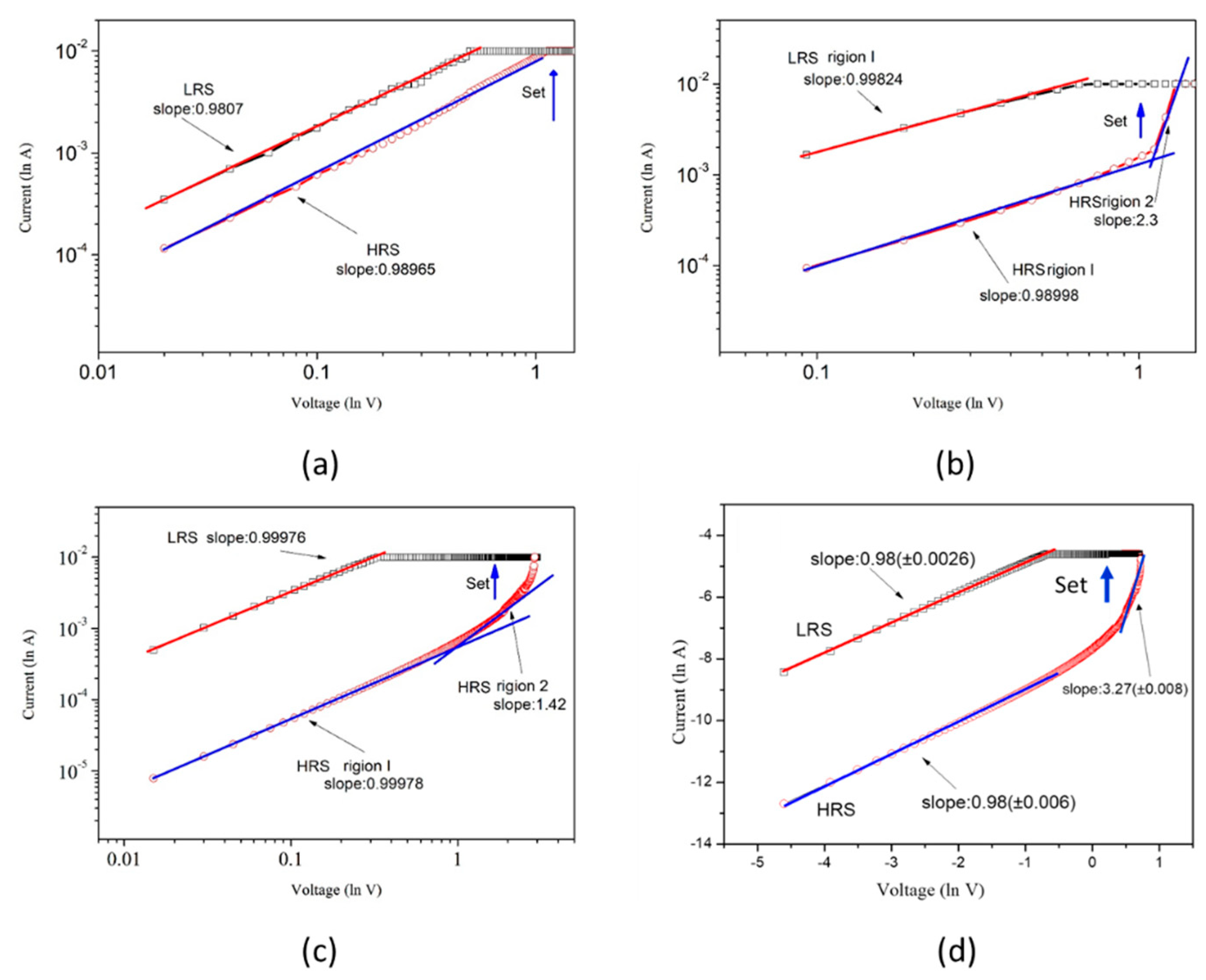
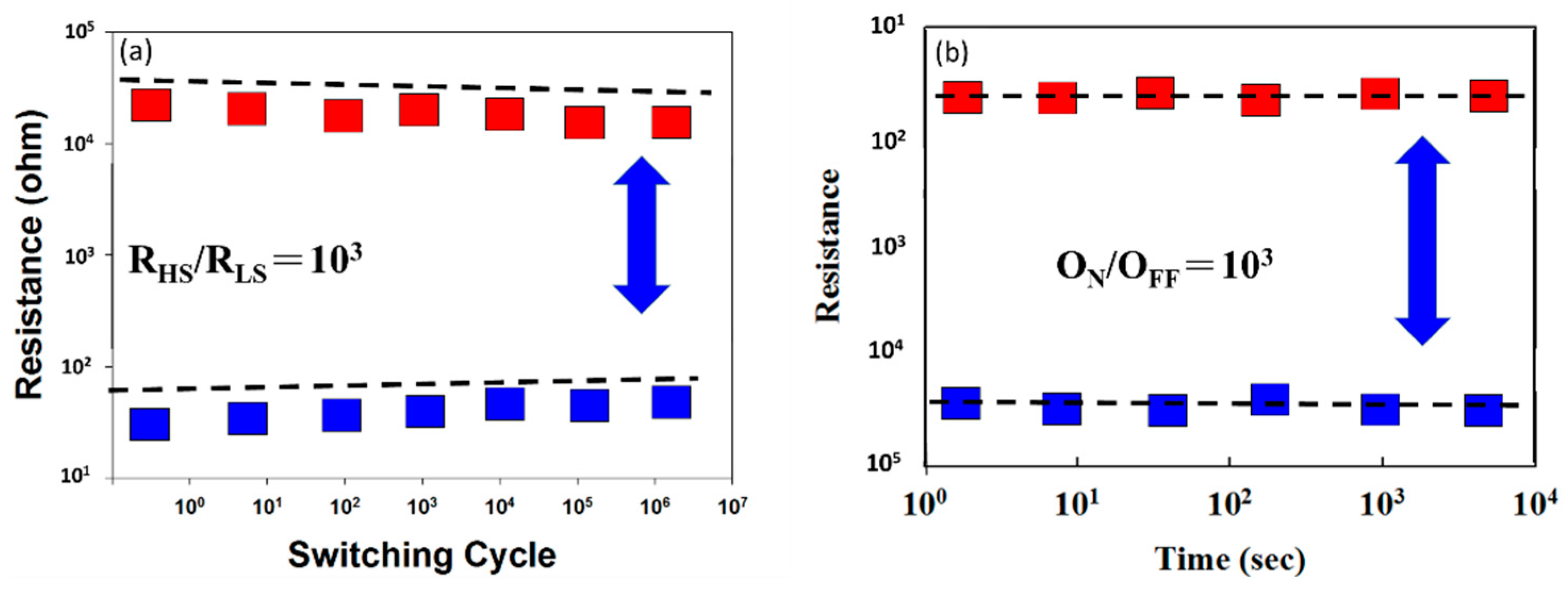
3. Results and Discussion

Figure 2 displays the XRD for Zn1−xCuxO with various Cu concentrations, compared with the pure zinc oxide. The XRD patterns match the standard JCPDS data (36-1451), indicating the absence of a rutile phase or any other phase. All samples have a wurtzite hexagonal structure oriented along the c-axis and a symmetric P63/mc structure. There is no evidence of phase separation in the Zn1−xCuxO thin films with the replacement of Zn with Cu ions. In addition, there are no diffraction peaks of other impurities or compounds, indicating that copper ions have been doped into the ZnO lattice to replace zinc ions. The (002) peak intensity of Zn1−xCuxO films increases with the Cu doping content from 2% to 6%. The samples exhibit a (002) peak of ZnO at approximately 2θ = 34.5°. The enhanced (002) peak intensity with a higher Cu concentration can be attributed to lattice strain introduced by the size difference between Cu and Zn ions when Cu ions replace Zn ions in the ZnO lattice. The increased intensity of the (002) diffraction peak at approximately 2θ = 34.5° indicates a more ordered and periodic arrangement of atoms in the lattice along the c-axis. Lattice strain caused by the size mismatch between copper and zinc ions leads to this increase in order. When the atomic planes along the c-axis are more regularly spaced, the X-rays diffract more efficiently, resulting in higher intensity peaks in the XRD pattern. Strain affects the crystal structure and orientation of ZnO, resulting in greater distortion and increased (002) peak intensity as the Cu concentration rises.
FWHM reflects the change in the average size of Zn1−xCuxO grains. The grain size of Zn1−xCuxOdecreases with increasing FWHM. Specifically, a slight increase in FWHM was observed as the Cu concentration increased from 0% to 6%. Average sizes of grains for films, calculated using the Scherrer formula, were 20.3 nm for 0%, 15.2 nm for 2%, 9.5 nm for 4%, and 8.6 nm for 6%, respectively [23]. Figure 3 displays the surface morphology of theZn1−xCuxO films, showing granular porous surfaces for all samples. It is evident that grain size decreases with the increase in the Cu concentration. This phenomenon can be attributed to the crystal structure and growth of the material. When copper is introduced into the zinc oxide lattice, copper (Cu) and zinc (Zn) have different atomic sizes and lattice constants, creating a lattice mismatch. The lattice mismatch in the Zn1−xCuxOfilm causes crystal strain in the crystal structure and hinders the growth of larger grains. In addition, the surface density of films increases as the Cu concentration rises. Furthermore, the thickness of all samples was found to be 500 nm.
Figure 4 shows the photoluminescence (PL) spectrum of Zn1−xCuxO at room temperature. The PL spectrum of ZnO exhibits two main components: one in the ultraviolet region and the other in the yellow-green visible region. The ultraviolet emission band at 385 nm shows the transition of electrons from the bottom of the conduction band to the zinc vacancy energy level [24,25]. Multiple yellow–green emissions observed in Zn1−xCuxO films are attributed to oxygen vacancy defects, which correspond to the transition from the conduction band to oxygen vacancy defects [26]. The ultraviolet emission at 385 nm of the Zn1−xCuxO thin film increases as the copper content increases. This may be due to the copper doping causing more zinc vacancy energy levels in the ZnO thin film, which enhances the ultraviolet emission. In addition, the yellow–green light emission of Zn1−xCuxO thin film increases with the increase in the copper doping amount. This enhancement may be caused by the replacement of copper ions into the ZnO lattice to form Zn1−xCuxO, and more copper ions generate more oxygen vacancy defects in zinc oxide. Therefore, the transition from the conduction band to oxygen vacancy defects will also increase, resulting in an increase in yellow–green light emission in the Zn1−xCuxO thin film.
Transmission spectra with a range of 300–800 nm for Zn1−xCuxO are shown in Figure 5. As the doping of Cu increases from 0% to 6%, the light transmittance for the Zn1−xCuxO film decreases from 92% to 78%. To determine the absorption coefficient and bandgap of these films, graphical methods were employed. The value of (αhυ)2 can be obtained from the equation αhυ = A(hυ-Eg)n. In addition, the value of α can be obtained using the equation α = –(1/D)lnT [27], where T is the transmittance, A is a function of the refractive index and hole/electron effective masses, h is the constant of Planck, v is the frequency of photons, and Eg is the bandgap. For a direct bandgap semiconductor (n = 1/2), the bandgaps of all films were calculated via the extrapolation of the straight portion for the curve of (αhυ)2 = 0 in Figure 6.The inset of Figure 6 shows the relationship between the Cu doping amount and sample band gap energy. As the Cu content increases from 0 to 6%, the bandgap inZn1−xCuxOfilms decreases from 3.285 eV to 3.271 eV. This phenomenon may be attributed to the change in the energy band structure in the ZnO film when Cu ions are incorporated into the ZnO lattice. An exchange interaction occurs between the valence band/conduction band electrons of ZnO and the local d-electrons of Cu ions replacing Zn ions. This exchange interaction introduces a new shallow energy level between the valence band and conduction band of ZnO, resulting in a reduction in the band gap of ZnO [28]. The transmittance decreases with increased Cu content, and the bandgap energy reduces as Cu content increases. The observed correlation between the bandgap and Cu content is likely influenced by the microstructure changes arising from the incorporation of Cu ions.
Figure 7 illustrates the bipolar I-V switching curves of Zn1−xCuxO films during the initial formation at 5 V in RRAM, with green arrows indicating the direction of the voltage sweep. The compliance current is controlled at 10 mA. RRAM devices can be operated using LRS-HRS switching cycles up to 100 times without losing the electric properties. The real image of Zn1−xCuxO films’ RRAM device is shown in Figure 7a. The RRAM setup process involves shifting the device into the LRS with a high forward bias of the control voltage. The reset process is to reduce the operating current of the LRS and provide a negative bias voltage to the reset voltage to transition to the HRS state, showing a bipolar resistance change characteristic. According to the bipolar I-V switching curve of the Zn1−xCuxO film in Figure 7, the set voltages are 1.1V (0%), 1.2V (2%), 3V (4%), and 1.5V (6%), respectively. In addition, the rest voltages are −0.9V (0%), −1.4V (2%), −2.8V (4%), and −1.5V (6%), respectively. The LRS and HRS properties of RRAM can be explained by the formation and destruction of conductive filaments composed of oxygen vacancies [2,3,4,5]. The switching of RRAM can be explained by two resistance states (HRS and LRS), the basic mechanism of which is shown in Figure 8. The SET process is initiated when an external positive voltage is applied to the top electrode (Ag), as shown in Figure 8. During this process, oxygen anions (O2−) migrate away from their original sites towards the top electrode, creating oxygen vacancies in their place. As these oxygen vacancies cluster together, they align and form conductive filaments between the top and bottom electrodes, switching the RRAM device from HRS to LRS. Conversely, the RESET process occurs when the polarity of the applied bias voltage is changed, leading to the breaking of conductive filaments in the HRS state. Some partially occupied oxygen vacancies below the top electrode are refilled with oxygen anions, converting them back into regular oxygen sites. Figure 7 provides a comparison of the switched resistance properties for Zn1−xCuxO thin films in RRAM devices at different Cu concentrations. The RRAM device with 6% exhibits the highest ratio of LRS/HRS and a higher value of resistance in a state of HRS. When an external positive voltage is applied to the top electrode, the oxygen vacancies gather and arrange to connect the top and bottom metal electrodes, and electrons can be transferred near the oxygen vacancies by hopping, thus forming a conductive filament. On the contrary, when the polarity of the applied bias voltage is changed, some partially occupied oxygen vacancies under the top electrode are refilled by oxygen anions, resulting in the destruction of the oxygen vacancies forming the conductive filament. At this time, the device will change from a high current state to a low current state. The higher the number of destroyed oxygen vacancies, the higher the LRS/HRS ratio will be. Therefore, the highest LRS/HRS ratio of the 6% RRAM device should be attributed to the formation of conductive filaments and the destruction of more oxygen vacancies in 6% Cu-doped ZnO. The higher the number of oxygen vacancies destroyed, the lower the low current state, and, thus, the higher the LRS/HRS ratio. In addition, the grain size of Zn1−xCuxO decreases with increasing Cu doping in the SEM analysis, which means there are more grain boundaries within the material. The grain boundaries typically exhibit higher electrical conductivity than the interior of grains in polycrystalline materials. The doping of copper can promote the formation of carrier transmission paths at the grain boundaries of Zn1−xCuxO and can also increase the carrier concentration within the Zn1−xCuxO material. This means that more carriers are available for transmission, which can lead to a lower resistive resistance state (LRS) and, thus, improve the LRS/HRS ratio and enhance the switching performance [29].
Figure 9 displays the lnI versus lnV plot of the Zn1−xCuxO thin film, which is used to analyze the carrier conduction mechanism and understand the initial conductive filament formation process in the set/reset states of a metal–insulator–metal (MIM) structure. In the set state, the conduction path of the filaments is primarily influenced by the presence of oxygen vacancies in the Cu-doped ZnO films. The IV curves for the low resistance state (LRS) of all samples show slopes of approximately 0.98–0.99, indicating an ohmic conduction mechanism where the current is linearly dependent on the applied voltage. As the voltage increases, a stepwise increase in current is observed. On the other hand, in Figure 9b–d, the curves’ slopes in the high electric field region of the high resistance state (HRS) are approximately 7.27–8.2, and the current rises sharply with the voltage. This suggests that the accumulation of oxygen vacancies in Cu-doped ZnO films enables carriers to be transported through traps located at different energy levels, leading to the trap-assisted tunneling (TAT) mechanism responsible for this IV behavior [30,31,32]. Current density dominated by TAT can be expressed as:
J T A T = A E 2 e x p [ B E ]
A = q 3 m 16 π 2 m * ϕ t
B = 4 2 m * 3 q ϕ t 3 / 2
where m * is the effective mass of the electron, ℏ is Planck’s constant, m is the mass of the electron in free space, and ϕt is the barrier height of the trap.
From the above results, the switching retention and endurance characteristics of the 6% Cu-doped ZnO thin film RRAM device are shown in Figure 10. It can be seen from the results that the 6% Cu-doped ZnO thin film RRAM device exhibits a stable state in more than one million switching cycles in Figure 10a. And the relationship between the resistance and switching time between the HRS and LRS states of the RRAM device can be clearly observed. RRAM devices also exhibit typical bipolar switching behavior and memory ratios greater than 103 HRS/LRS. In addition, the endurance characteristics of the 6% Cu-doped ZnO thin film RRAM device are shown in Figure 10b. There is no significant change in the on/off ratio switching behavior cycling versus time curves of the RRAM device over 103 s.

4. Conclusions

Zn1−xCuxO films were deposited on FTO substrates fabricated using the sol-gel process. The crystal structure, optical and resistive switching properties of Zn1−xCuxO were studied and analyzed. The intensity of the (002) peaks of the Zn1−xCuxO increased with an increase in doping of Cu from x=0 to x=0.06. Moreover, as the Cu content increased, the intensity of the ultraviolet emission and the yellow–green light emission peaks increased in the photoluminescence spectrum of Zn1−xCuxO film. It was found that the Zn1−xCuxO thin film RRAM exhibits the ohmic conduction mechanism and the trap-assisted tunneling (TAT) mechanism in the low electric field region (LRS) and high electric field region (HRS), respectively. RRAM devices based on 6% Cu-doped ZnO films exhibited the highest LRS/HRS ratio and higher HRS state resistance.

Author Contributions

M.-C.K. and J.-H.W. conceived and designed the experiments. M.-Z.L. prepared the materials. M.-C.K. and M.-Z.L. performed the experiments. M.-C.K. and K.-H.C. analyzed the data. M.-C.K. and J.-H.W. wrote the manuscript. All authors have read and agreed to the published version of the manuscript.

Funding

This work was supported by the National Science Council of the Republic of China under Contract No. NSC MOST 111-2637-E-164-002.

Data Availability Statement

Not applicable.

Conflicts of Interest

The founding sponsors had no role in the design of the study; in the collection, analyses, or interpretation of data; in the writing of the manuscript, and in the decision to publish the results.

Correction Statement

This article has been republished with a minor correction to remove a duplicated Figure 5. This change does not affect the scientific content of the article.

References

  1. Li, Y.T.; Long, S.B.; Zhang, M.H.; Liu, Q.; Shao, L.B.; Zhang, S.; Wang, Y.; Zuo, Q.Y.; Liu, S.; Liu, M. Resistive switching properties of Au/ZrO2/Ag structure for low-voltage nonvolatile memory applications. IEEE Electron. Device Lett. 2010, 31, 117–119. [Google Scholar]
  2. Guo, Y.; Robertson, J. Materials selection for oxide-based resistive random access memories. Appl. Phys. Lett. 2014, 105, 223516–223518. [Google Scholar] [CrossRef]
  3. Puglisi, F.M.; Larcher, L.; Bersuker, G.; Padovani, A.; Pavan, P. An empirical model for RRAM resistance in low- and high-resistance states. IEEE Electron Device Lett. 2013, 34, 387–389. [Google Scholar] [CrossRef]
  4. Zhuge, F.; Peng, S.; He, C.; Zhu, X.; Chen, X.; Liu, Y.; Li, R. Improvement of resistive switching in Cu/ZnO/Pt sandwiches by weakening the randomicity of the formation/rupture of Cu filaments. Nanotechnology 2011, 22, 275204–275208. [Google Scholar] [CrossRef]
  5. Ke, J.J.; Wei, T.C.; Tsai, D.S.; Lin, C.H.; He, J.H. Surface effects of electrode-dependent switching behavior of resistive random-access memory. Appl. Phys. Lett. 2016, 109, 131603–131606. [Google Scholar] [CrossRef]
  6. Chang, W.-Y.; Lai, Y.-C.; Wu, S.-F.; Wang, F.; Chen, F.; Tsai, M.-J.; Tsai, M.-J. Unipolar resistive switching characteristics of ZnO thin films for nonvolatile memory applications. Appl. Phys. Lett. 2008, 92, 022110–022113. [Google Scholar] [CrossRef]
  7. Xu, N.; Liu, L.; Sun, X.; Liu, X.; Han, D.; Wang, Y.; Han, R.; Kang, J.; Yu, B. Characteristics and mechanism of conduction/set process in TiNZnOPt resistance switching random-access memories. Appl. Phys. Lett. 2008, 92, 92232112–92232113. [Google Scholar] [CrossRef]
  8. Kim, S.; Moon, H.; Gupt, D.; Yoo, S.; Choi, Y.K. Resistive Switching Characteristics of Sol–Gel Zinc Oxide Films for Flexible Memory Applications. IEEE Electron. Device Lett. 2009, 56, 696–699. [Google Scholar] [CrossRef]
  9. Villafuerte, M.; Heluani, S.P.; Juarez, G.; Simonelli, G.; Braunstein, G.; Duhalde, S. Electric-pulse-induced reversible resistance in doped zinc oxide thin film. Appl. Phys. Lett. 2007, 90, 052105. [Google Scholar] [CrossRef]
  10. Zhang, X.T.; Liu, Y.C.; Zhang, J.Y.; Lu, Y.M.; Shen, D.Z.; Fan, X.W.; Kong, X.G. Structure and photoluminescence of Mn-passivated nanocrystalline ZnO thin films. J. Cryst. Growth 2003, 254, 80–85. [Google Scholar] [CrossRef]
  11. Xu, H.T.; Kim, D.H.; Zhao, X.H.; Ying, L.; Zhu, M.Y.; Lee, B.; Liu, C. Effect of Co doping on unipolar resistance switching in Pt/Co:ZnO/Pt structures. J. Alloys Compd. 2016, 658, 806–812. [Google Scholar] [CrossRef]
  12. He, S.; Hao, A.; Qin, N.; Bao, D. Unipolar resistive switching properties of Pr-doped ZnO thin films. Ceram. Int. 2017, 43, S474–S480. [Google Scholar] [CrossRef]
  13. Xu, D.; Xiong, Y.; Tang, M.; Zeng, B. Top electrode-dependent resistance switching behaviors of lanthanum-doped ZnO film memory devices. Appl. Phys. A 2014, 114, 1377–1381. [Google Scholar] [CrossRef]
  14. Chiu, F.C.; Yang, M.Y. Trap characterization and conductance quantization in phosphorus-doped ZnO memory devices. Vacuum 2017, 140, 42–46. [Google Scholar] [CrossRef]
  15. Zhu, X.J.; Su, W.J.; Liu, Y.W.; Hu, B.L.; Pan, L.; Lu, W.; Zhang, J.D.; Li, R.W. Observation of Conductance Quantization in Oxide-Based Resistive Switching Memory. Adv. Mater. 2012, 24, 3941–3946. [Google Scholar] [CrossRef]
  16. Peng, H.Y.; Li, G.P.; Ye, J.Y.; Wei, Z.P.; Zhang, Z.; Wang, D.D.; Xing, G.Z.; Wu, T. Electrode dependence of resistive switching in Mn-doped ZnO: Filamentary versus interfacial mechanisms. Appl. Phys. Lett. 2010, 96, 192113–192115. [Google Scholar] [CrossRef]
  17. Yang, Y.C.; Pan, F.; Liu, Q.; Liu, M.; Zeng, F. Fully Room-Temperature-Fabricated Nonvolatile Resistive Memory for Ultrafast and High-Density Memory Application. Nano Lett. 2009, 9, 1636–1643. [Google Scholar] [CrossRef]
  18. Dietl, T.; Ohno, H.; Matsukura, F.; Cibert, J.; Ferrand, D. Zener model description of ferromagnetism in zinc-blende magnetic semiconductors. Science 2000, 287, 1019–1022. [Google Scholar] [CrossRef]
  19. Wu, L.; Hou, T.J.; Wang, Y.; Zhao, Y.F.; Guo, Z.Y.; Li, Y.Y.; Lee, S.T. First-principles study of doping effect on the phase transition of zinc oxide with transition metal doped. J. Alloys Compd. 2012, 541, 250–255. [Google Scholar] [CrossRef]
  20. Iribarren, A.; Hernandez-Rodriguez, E.; Maqueira, L. Structural, chemical and optical evaluation of Cu-doped ZnO nanoparticles synthesized by an aqueous solution method. Mater. Res. Bull. 2014, 60, 376–381. [Google Scholar] [CrossRef]
  21. Mohan, R.; Krishnamoorthy, K.; Kim, S.J. Enhanced photocatalytic activity of Cu-doped ZnO nanorods. Solid State Commun. 2012, 152, 375–380. [Google Scholar] [CrossRef]
  22. Srinivasan, N.; Revathi, M.; Pachamuthu, P. Surface and optical properties of undoped and Cu doped ZnO nanostructures. Optik 2017, 130, 422–426. [Google Scholar] [CrossRef]
  23. Hull, A.W. A new method of X-ray crystal analysis. Phys. Rev. 1917, 10, 661–696. [Google Scholar] [CrossRef]
  24. Patil, V.L.; Vanalakara, S.A.; Patil, P.S.; Kim, J.H. Fabrication of nanostructured ZnO thin films based NO2 gas sensor via SILAR technique. Sens. Actuators B Chem. 2017, 239, 1185–1193. [Google Scholar] [CrossRef]
  25. Singh, M.; Ambedkar, A.K.; Tyagi, S.; Kumar, V.; Yadav, P.; Kumar, A.; Gautam, Y.K.; Singh, B.P. Room temperature photoluminescence and spectroscopic ellipsometry of reactive co-sputtered Cu-doped ZnO thin films. Optik 2022, 257, 168860–168871. [Google Scholar] [CrossRef]
  26. Mustafa, G.; Srivastava, S.; Aziz, M.K.; Kanaoujiya, R.; Rajkumar, C. Photosensitivity and structural properties of vanadium-doped ZnO and ZnO nanoparticle at various calcined temperature. Mater. Today Proc. 2023; online ahead of print. [Google Scholar] [CrossRef]
  27. Ma, L.; Ai, X.; Huang, X.; Ma, S. Effects of the substrate and oxygen partial pressure on the microstructure and optical properties of Ti-doped ZnO thin films. Superlattices Microstruct. 2011, 50, 703–712. [Google Scholar] [CrossRef]
  28. Ghorbali, R.; Essalah, G.; Ghoudi, A.; Guermazi, H.; Guermazi, S.; El Hdiy, A.; Benhayoune, H.; Duponchel, B.; Oueslati, A.; Leroy, G. The effect of (In, Cu) doping and co-doping on physical properties and organic pollutant photodegradation efficiency of ZnO nanoparticles for wastewater remediation. Ceram. Int. 2023, 49, 33828–33841. [Google Scholar] [CrossRef]
  29. Deuermeier, J.; Wardenga, H.F.; Morasch, J.; Siol, S.; Nandy, S.; Calmeiro, T.; Klein, A.; Fortunato, E. Highly conductive grain boundaries in copper oxide thin films. J. Appl. Phys. 2016, 119, 235303–235308. [Google Scholar] [CrossRef]
  30. Hsu, C.C.; Chen, Y.T.; Chuang, P.Y.; Lin, Y.S. Abnormal volatile memory characteristic in normal nonvolatile ZnSnO resistive switching memory. IEEE Trans. Electron. Devices 2018, 65, 2812–2819. [Google Scholar] [CrossRef]
  31. Chanana, R.K. Determination of electron and hole effective masses in thermal oxide utilizing an n-channel silicon MOSFET. IOSR J. Appl. Phys. 2014, 6, 1–7. [Google Scholar] [CrossRef]
  32. Yu, S.; Guan, X.; Wong, H.-S.P. Conduction mechanism of TiN/HfOx/Pt resistive switching memory: A trap-assisted-tunneling model. Appl. Phys. Lett. 2011, 99, 063507. [Google Scholar] [CrossRef]
Figure 1. RRAM structure of Ag/Zn1−xCuxO/FTO.
Nanomaterials 13 02685 g001
Figure 2. The patterns of XRD for Zn1−xCuxO films.
Nanomaterials 13 02685 g002
Figure 3. The images of SEM for Zn1−xCuxO films of (a) x = 0, (b) x = 2%, (c) x = 4%, and (d) x = 6%.
Nanomaterials 13 02685 g003
Figure 4. Photoluminescence (PL) spectra of Zn1−xCuxO films of (a) x = 0, (b) x = 2%, (c) x = 4%, and (d) x = 6%.
Nanomaterials 13 02685 g004
Figure 5. Spectra of optical transmittance for Zn1−xCuxO.
Nanomaterials 13 02685 g005
Figure 6. The curves of (αhυ)2 vs. Eg for Zn1−xCuxO. The inset is Cu doping amount vs. bandgap energy.
Nanomaterials 13 02685 g006
Figure 7. The switching curves of I–V of Zn1−xCuxO RRAM of (a) x = 0, (b) x = 2%, (c) x = 4%, and (d) x = 6% (inset shows the real device image in (a)).
Nanomaterials 13 02685 g007
Figure 8. Schematic diagram of mechanisms of LRS and HRS for Ag/Zn1−xCuxO/FTO RRAM device.
Nanomaterials 13 02685 g008
Figure 9. The curves of I–V for Zn1−xCuxO RRAM for the lnI–lnV curve of (a) x = 0, (b) x = 2%, (c) x = 4%, and (d) x = 6%.
Nanomaterials 13 02685 g009
Figure 10. Switching endurance results of 6% Cu-doped ZnO film RRAM device showing (a) retention properties and (b) endurance properties.
Nanomaterials 13 02685 g010
Disclaimer/Publisher’s Note: The statements, opinions and data contained in all publications are solely those of the individual author(s) and contributor(s) and not of MDPI and/or the editor(s). MDPI and/or the editor(s) disclaim responsibility for any injury to people or property resulting from any ideas, methods, instructions or products referred to in the content.

