
Effect of Electrochemically Active Top Electrode Materials on Nanoionic Conductive Bridge Y2O3 Random-Access Memory
 ,
,  , , , and
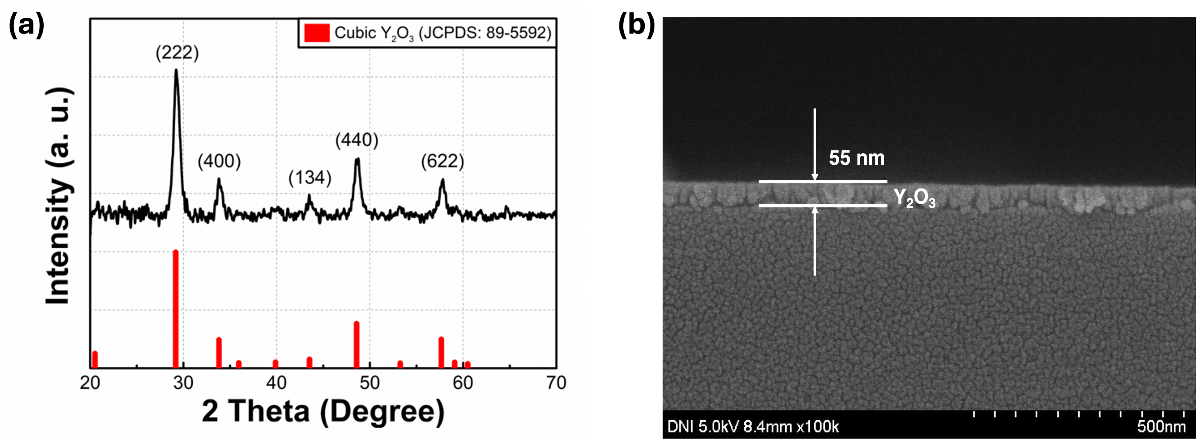
Abstract
:1. Introduction
2. Materials and Methods
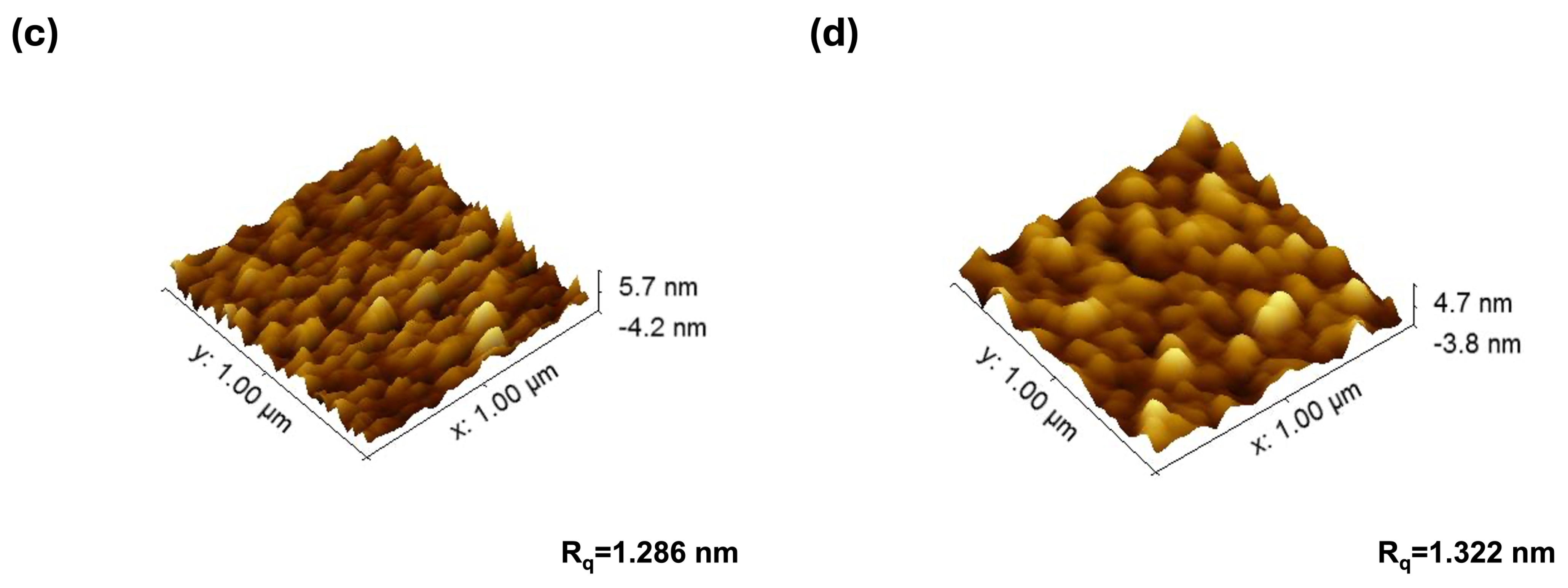
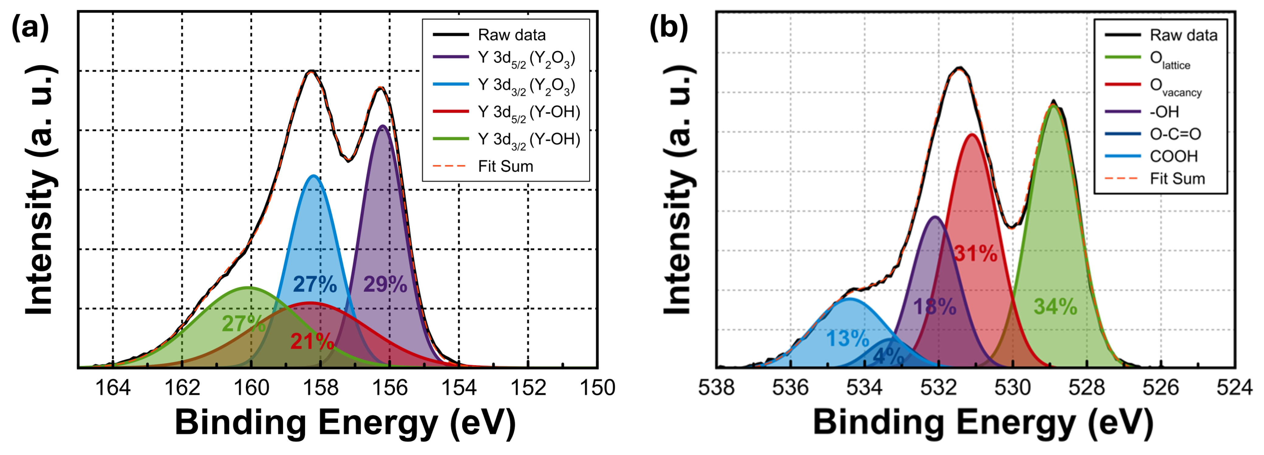
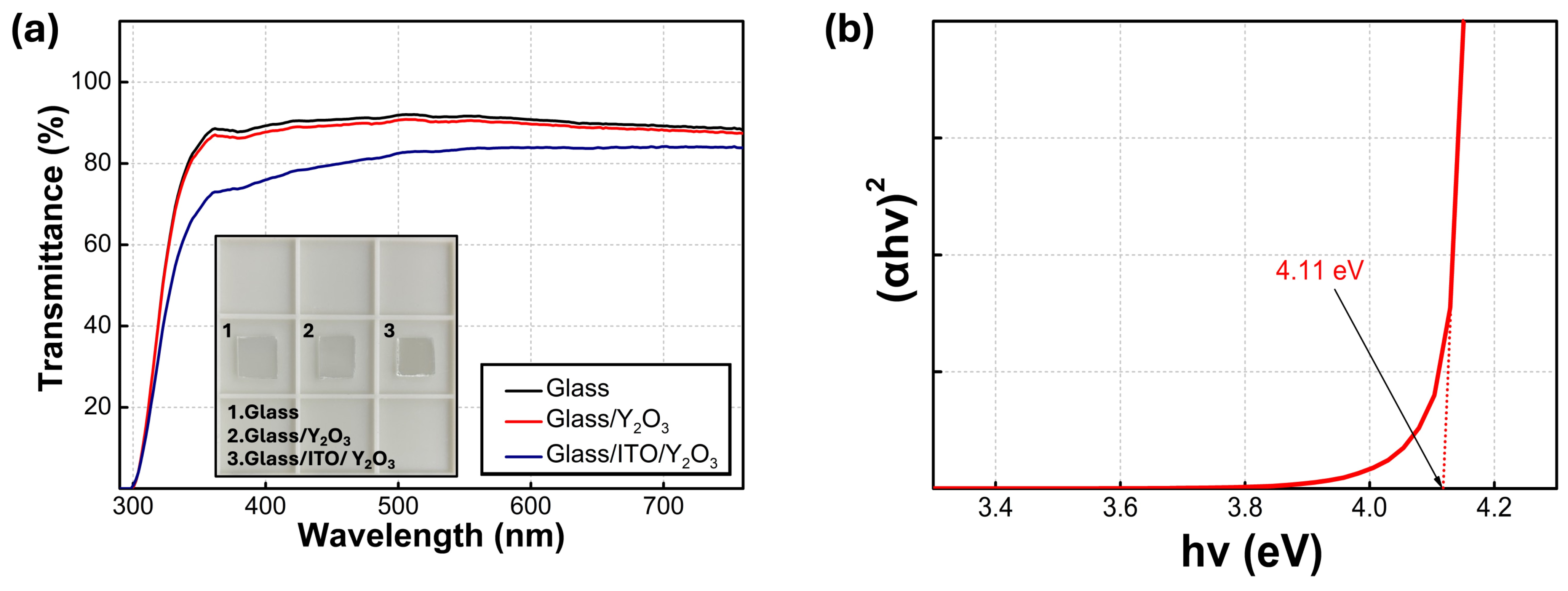
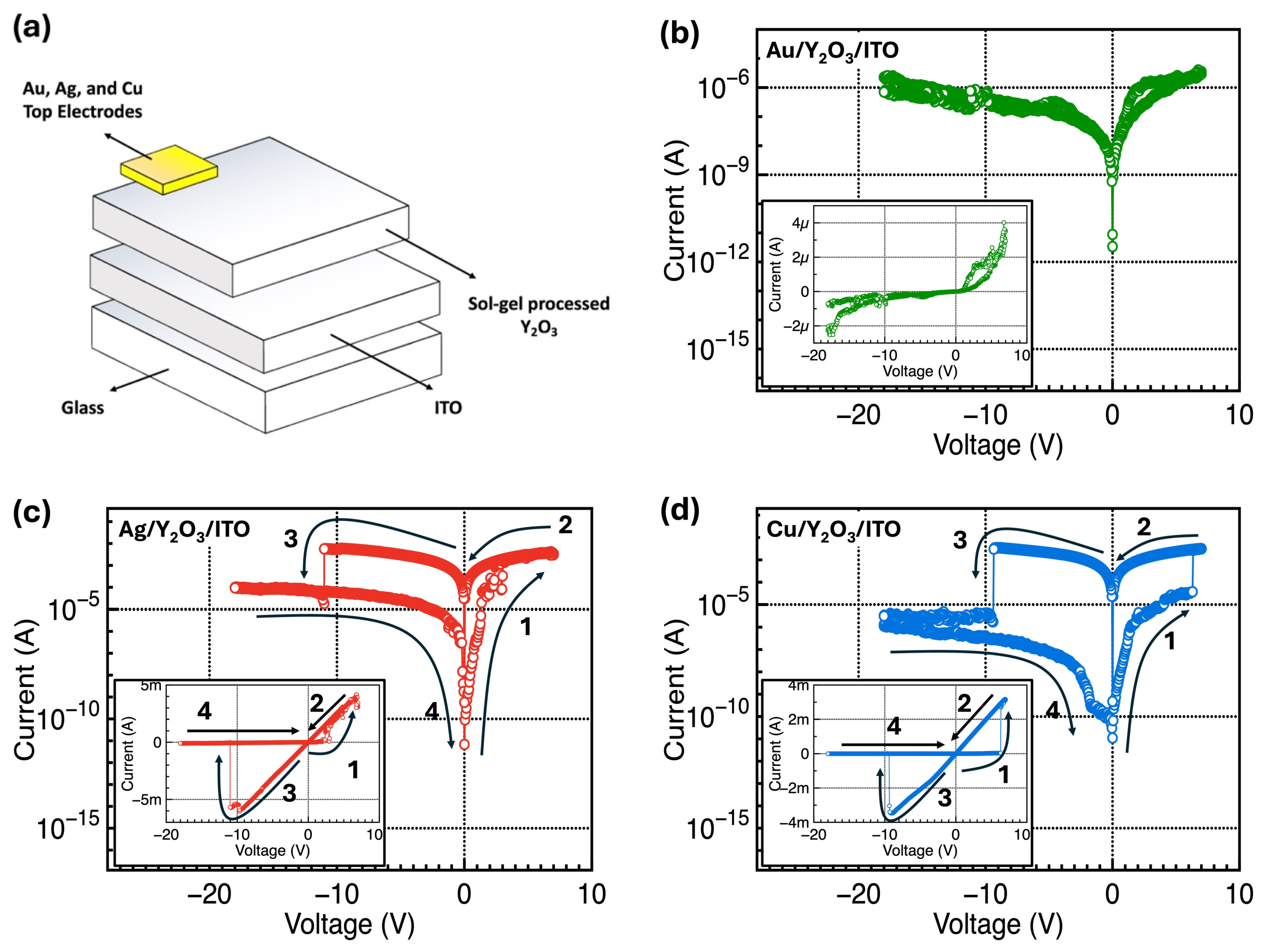
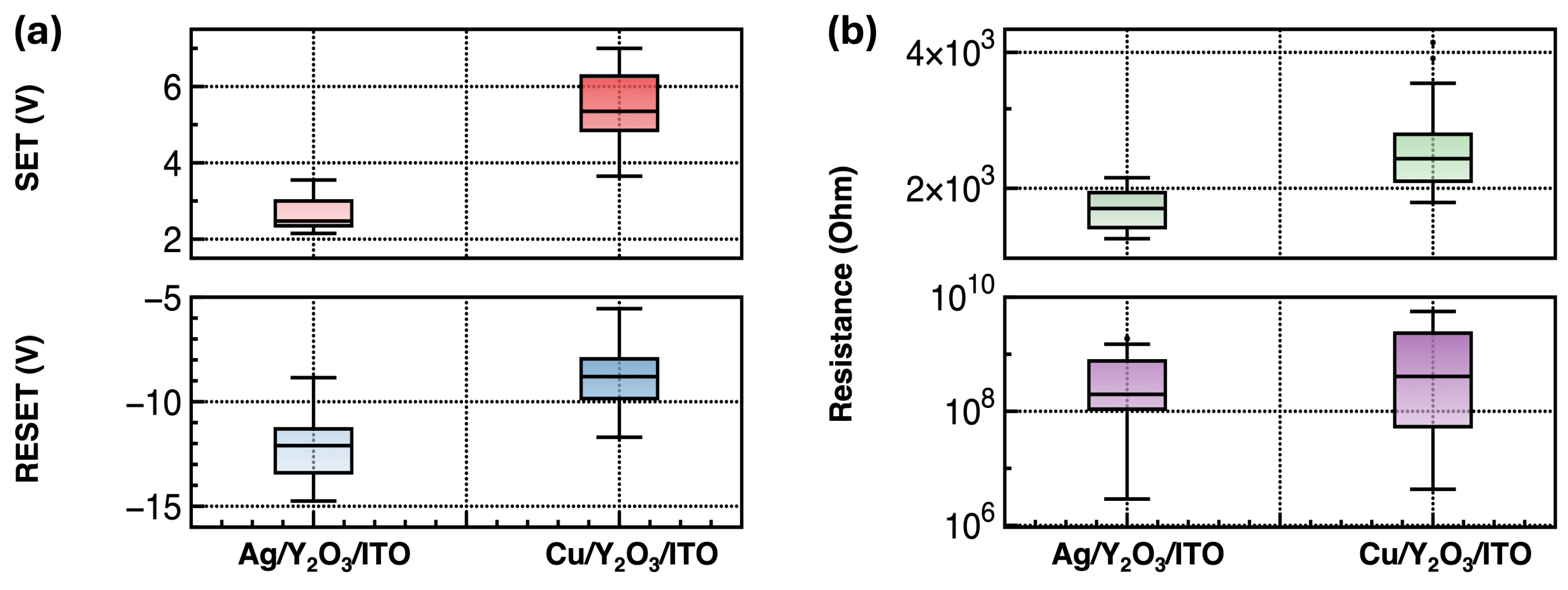
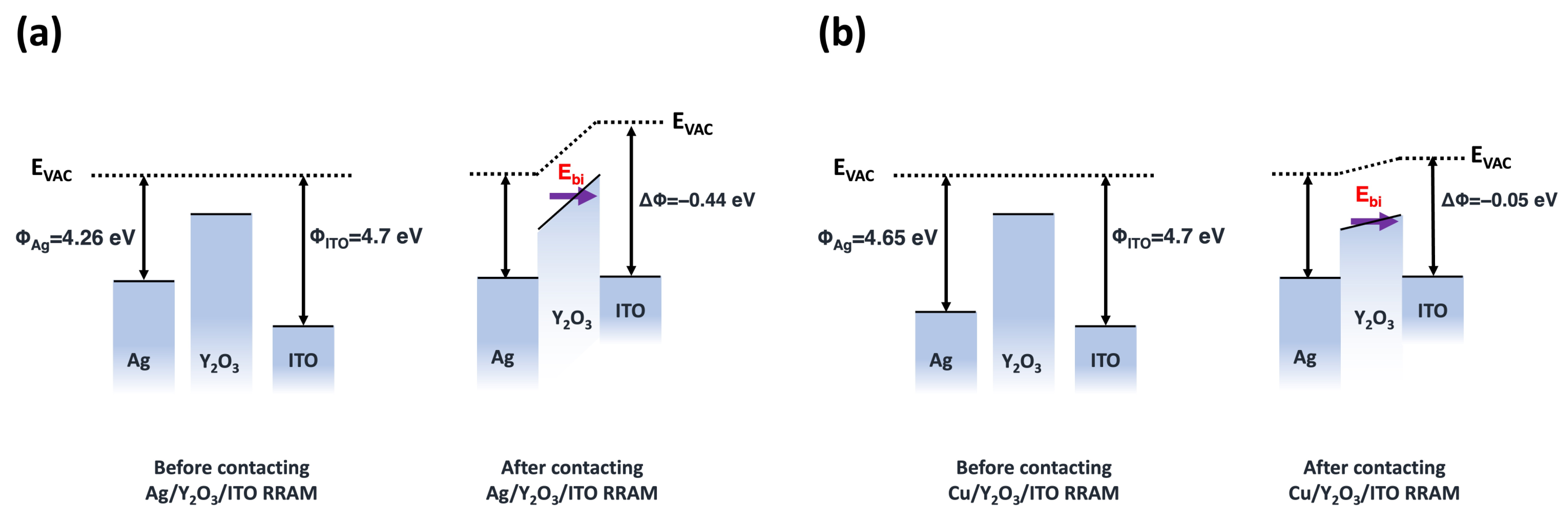
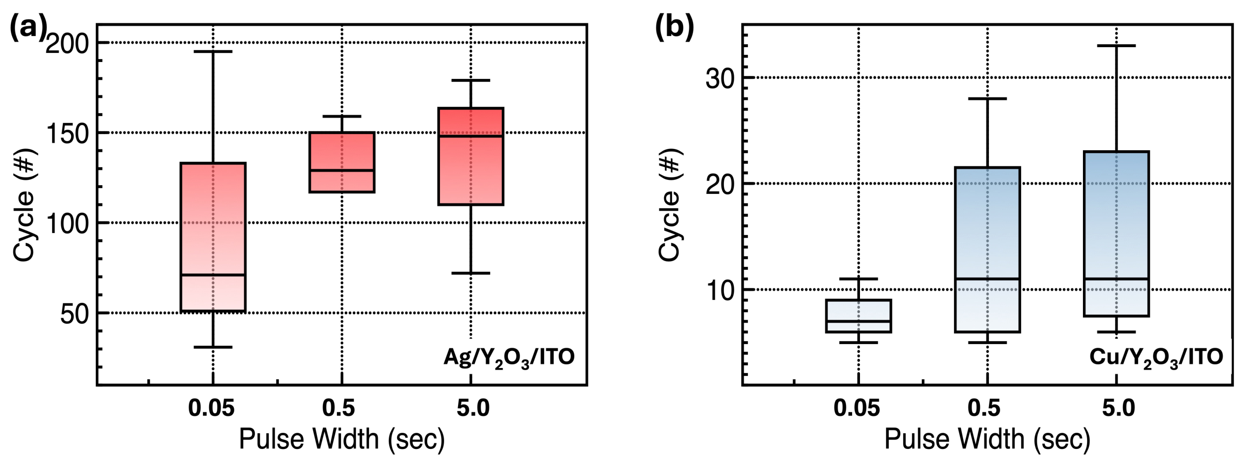
3. Results and Discussion
4. Conclusions
Author Contributions
Funding
Data Availability Statement
Conflicts of Interest
References
- Chandrasekaran, N. Challenges in 3D Memory Manufacturing and Process Integration. In Proceedings of the 2013 IEEE International Electron Devices Meetin, Washington, DC, USA, 9–11 December 2013. [Google Scholar]
- Wang, Z.; Joshi, S.; Savel’ev, S.E.; Jiang, H.; Midya, R.; Lin, P.; Hu, M.; Ge, N.; Strachan, J.P.; Li, Z. Memristors with Diffusive Dynamics as Synaptic Emulators for Neuromorphic Computing. Nat. Mater. 2017, 16, 101–108. [Google Scholar] [CrossRef]
- Yoon, J.H.; Wang, Z.; Kim, K.M.; Wu, H.; Ravichandran, V.; Xia, Q.; Hwang, C.S.; Yang, J.J. An Artificial Nociceptor based on a Diffusive Memristor. Nat. Commun. 2018, 9, 417. [Google Scholar] [CrossRef]
- Jeong, D.S.; Hwang, C.S. Nonvolatile Memory Materials for Neuromorphic Intelligent machines. Adv. Mater. 2018, 30, 1704729. [Google Scholar] [CrossRef]
- Lee, T.; Kim, H.I.; Cho, Y.; Lee, S.; Lee, W.Y.; Bae, J.H.; Kang, I.M.; Kim, K.; Lee, S.H.; Jang, J. Sol–Gel-Processed Y2O3 Multilevel Resistive Random-Access Memory Cells for Neural Networks. Nanomaterials 2023, 13, 2432. [Google Scholar] [CrossRef]
- Wiśniewski, P.; Nieborek, M.; Mazurak, A.; Jasinski, J. Investigation of the Temperature Effect on Electrical Characteristics of Al/SiO2/n++-Si RRAM Devices. Micromachines 2022, 13, 1641. [Google Scholar] [CrossRef]
- Jang, J.; Subramanian, V. Effect of Electrode Material on Resistive Switching Memory Behavior of Solution-processed Resistive Switches: Realization of Robust Multi-level Cell. Thin Solid Films 2017, 625, 87–92. [Google Scholar] [CrossRef]
- Brivio, S.; Spiga, S.; Ielmini, D. HfO2-based Resistive Switching Memory Devices for Neuromorphic Computing. Neuromorph. Comput. Eng. 2022, 2, 042001. [Google Scholar] [CrossRef]
- Ding, Z.; Feng, Y.; Huang, P.; Liu, L.; Kang, J. Low-power Resistive Switching Characteristic in HfO2/TiOx Bilayer Resistive Random-access Memory. Nanoscale Res. Lett. 2018, 14, 157. [Google Scholar] [CrossRef]
- Carta, D.; Salaoru, I.; Khiat, A.; Regoutz, A.; Mitterbauer, C.; Harrison, N.M.; Prodromakis, T. Investigation of the Switching Mechanism in TiO2-Based RRAM: A Two-Dimensional EDX Approach. ACS Appl. Mater. Interfaces 2016, 8, 19605–19611. [Google Scholar] [CrossRef]
- Das, M.; Kumar, A.; Mandal, B.; Htay, M.T.; Mukherjee, S. Impact of Schottky Junctions in the Transformation of Switching Modes in Amorphous Y2O3-based Memristive System. J. Phys. D Appl. Phys. 2018, 51, 315102. [Google Scholar] [CrossRef]
- Chiam, S.Y.; Chim, W.K.; Pi, C.; Huan, A.C.H.; Wang, S.J.; Pan, J.S.; Turner, S.; Zhang, J. Band Alignment of Yttrium Oxide on Various Relaxed and Strained Semiconductor Substrates. J. Appl. Phys. 2008, 103, 083702. [Google Scholar] [CrossRef]
- Rushchanskii, K.Z.; Blügel, S.; Ležaić, M. Ab initio phase diagrams of Hf-O, Zr-O and Y-O: A comparative study. Faraday Discuss. 2019, 213, 321–337. [Google Scholar] [CrossRef]
- Iwasawa, J.; Nishimizu, R.; Tokita, M.; Kiyohara, M.; Uematsu, K. Plasma-Resistant Dense Yttrium Oxide Film Prepared by Aerosol Deposition Process. J. Am. Ceram. Soc. 2007, 90, 2327–2332. [Google Scholar] [CrossRef]
- Fukabori, A.; Yanagida, T.; Pejchal, J.; Maeo, S.; Yokota, Y.; Yoshikawa, A.; Ikegami, T.; Moretti, F.; Kamada, K. Optical and scintillation characteristics of transparent ceramic. J. Appl. Phys. 2010, 107, 073501. [Google Scholar] [CrossRef]
- Kränkel, C. Rare-earth-doped sesquioixides for diode-pumped high-power lasers in the 1-, 2-, and 3-μm spectral range. IEEE J. Sel. Top. Quantum Electron. 2015, 21, 250–262. [Google Scholar] [CrossRef]
- Petzold, S.; Piros, E.; Sharath, S.U.; Zintler, A.; Hildebrandt, E.; Molina-Luna, L.; Wenger, C.; Alff, L. Gradual Reset and Set Characteristics in Yttrium Oxide based Resistive Random Access Memory. Semicond. Sci. Technol. 2019, 34, 075008. [Google Scholar] [CrossRef]
- Kim, K.; Kim, H.I.; Lee, T.; Lee, W.Y.; Bae, J.H.; Kang, I.M.; Lee, S.H.; Kim, K.; Jang, J. Thickness dependence of resistive switching characteristics of the sol–gel processed Y2O3 RRAM devices. Semicond. Sci. Technol. 2023, 38, 045002. [Google Scholar] [CrossRef]
- Pan, F.; Gao, S.; Chen, C.; Song, C.; Zeng, F. Recent Progress in Resistive Random Access Memories: Materials, Switching Mechanisms, and Performance. Mater. Sci. Eng. R Rep. 2014, 83, 1–59. [Google Scholar] [CrossRef]
- Wong, H.S.P.; Lee, H.Y.; Yu, S.; Chen, Y.S.; Wu, Y.; Chen, P.S.; Lee, B.; Chen, F.T.; Tsai, M.J. Metal–Oxide RRAM. Proc. IEEE 2012, 100, 1951–1970. [Google Scholar] [CrossRef]
- Waser, R.; Dittmann, R.; Staikov, G.; Szot, K. Redox-Based Resistive Switching Memories—Nanoionic Mechanisms, Prospects, and Challenges. Adv. Mater. 2009, 21, 2632–2663. [Google Scholar] [CrossRef]
- Hsu, C.C.; Liu, P.T.; Gan, K.J.; Ruan, D.B.; Sze, S.M. Oxygen Concentration Effect on Conductive Bridge Random Access Memory of InWZnO Thin Film. Nanomaterials 2021, 11, 2204. [Google Scholar] [CrossRef]
- Cho, H.; Kim, S. Emulation of Biological Synapse Characteristics from Cu/AlN/TiN Conductive Bridge Random Access Memory. Nanomaterials 2020, 10, 1709. [Google Scholar] [CrossRef]
- Lim, D.; Kwak, D.; Yi, J. Improved Interface Properties of Yttrium Oxide Buffer Layer on Silicon Substrate for Ferroelectric Random Access Memory Application. Thin Solid Films 2002, 422, 150–154. [Google Scholar] [CrossRef]
- de Rouffignac, P.; Park, J.S.; Gordon, R.G. Atomic Layer Deposition of Y2O3 Thin Films from Yttrium Tris (N,N′-diisopropylacetamidinate) and Water. Chem. Mater. 2005, 17, 4808–4814. [Google Scholar] [CrossRef]
- Boukhvalov, D.W.; Zatsepin, D.A.; Kuznetsova, Y.A.; Gavrilov, N.V.; Zatsepin, A.F. Comparative Analysis of the Electronic Energy Structure of Nanocrystalline Polymorphs of Y2O3 Thin Layers: Theory and Experiments. Appl. Surf. Sci. 2023, 613, 155935. [Google Scholar] [CrossRef]
- Lin, S.; Xu, Y.; Fu, C.; Zhang, H.; Kong, Q.; He, H.; Liu, S.; Shi, X.; Zhao, D. Novel Y2O3 based Calcium-Alginate Beads for Highly Selective Adsorption of Phosphate from Aqueous Solution. Environ. Sci. Pollut. Res. 2023, 30, 73534–73547. [Google Scholar] [CrossRef]
- Yuan, G.; Li, M.; Yu, M.; Tian, C.; Wang, G.; Fu, H. In Situ Synthesis, Enhanced Luminescence and Application in Dye Sensitized Solar Cells of Y2O3/Y2O2S:Eu3+ Nanocomposites by Reduction of Y2O3:Eu3+. Sci. Rep. 2016, 6, 37133. [Google Scholar] [CrossRef]
- Kim, M.J. A Study on Optimal Indium Tin Oxide Thickness as Transparent Conductive Electrodes for Near-Ultraviolet Light-Emitting Diodes. Materials 2023, 16, 4718. [Google Scholar] [CrossRef]
- Zhang, L.; Li, Z.; Zhen, F.; Wang, L.; Zhang, Q.; Sun, R.; Selim, F.A.; Wong, C.; Chen, H. High Sinterability Nano-Y2O3 Powders Prepared via Decomposition of Hydroxyl-carbonate Precursors for Transparent Ceramics. J. Mater. Sci. 2017, 52, 8556–8567. [Google Scholar] [CrossRef]
- Chen, W.F.; Koshy, P.; Sorrell, C.C. Effects of Film Topology and Contamination as a Function of Thickness on the Photo-Induced Hydrophilicity of Transparent TiO2 Thin Films Deposited on Glass Substrates by Spin Coating. J. Mater. Sci. 2016, 51, 2465–2480. [Google Scholar] [CrossRef]
- Xu, J.; Teng, Y.; Teng, F. Effect of Surface Defect States on Valence Band and Charge Separation and Transfer Efficiency. Sci. Rep. 2016, 6, 32457. [Google Scholar] [CrossRef]
- Yang, B.; Xu, N.; Li, C.; Huang, C.; Ma, D.; Liu, J.; Arumi, D.; Fang, L. A Forming-free ReRAM Cell with Low Operating Voltage. IEICE Electron. Express 2020, 17, 20200343. [Google Scholar] [CrossRef]
- Abbas, Y.; Ambade, R.B.; Ambade, S.B.; Han, T.H.; Choi, C. Tailored Nanoplateau and Nanochannel Structures using Solution-processed Rutile TiO2 Thin Films for Complementary and Bipolar Switching Characteristics. Nanoscale 2019, 11, 13815. [Google Scholar] [CrossRef]
- Bard, A.J.; Parsons, R.; Jordan, J. Standard Potentials in Aqueous Solution; Marcel Dekker: New York, NY, USA, 1985. [Google Scholar]
- Saadi, M.; Gonon, P.; Vallée, C.; Mannequin, C.; Grampeix, H.; Jalaguier, E.; Jomni, F.; Bsiesy, A. On the Mechanisms of Cation Injection in Conducting Bridge Memories: The Case of HfO2 in Contact with Noble Metal Anodes (Au, Cu, Ag). J. Appl. Phys. 2016, 119, 114501. [Google Scholar] [CrossRef]
- Tseng, Y.-T.; Chen, I.-C.; Chang, T.-C.; Huang, J.C.; Shih, C.-C.; Zheng, H.-X.; Chen, W.-C.; Wang, M.-H.; Huang, W.-C.; Chen, M.-C.; et al. Enhanced Electrical Behavior from the Galvanic Effect in Ag-Cu Alloy Electrode Conductive Bridging Resistive Switching Memory. Appl. Phys. Lett. 2018, 113, 053501. [Google Scholar] [CrossRef]
- Ho, T.L.; Ding, K.; Lyapunov, N.; Suen, C.H.; Wong, L.W.; Zhao, J.; Yang, M.; Zhou, X.; Dai, J.Y. Multi-Level Resistive Switching in SnSe/SrTiO3 Heterostructure Based Memristor Device. Nanomaterials 2022, 12, 2128. [Google Scholar] [CrossRef]
- Lee, K.J.; Wang, L.W.; Chiang, T.K.; Wang, Y.H. Effects of Electrodes on the Switching Behavior of Strontium Titanate Nickelate Resistive Random Access Memory. Materials 2015, 8, 7191–7198. [Google Scholar] [CrossRef]
- Chakraborty, A.; Al-Mamun, M.; Orlowski, M. Impact of Surface Roughness and Material Properties of Inert Electrodes on the Threshold Voltages and Their Distributions of ReRAM Memory Cells. ECS J. Solid State Sci. Technol. 2022, 11, 104007. [Google Scholar] [CrossRef]
- Cheun, H.; Fuentes-Hernandez, C.; Zhou, Y.; Potscavage, W.J., Jr.; Kim, S.J.; Shim, J.; Dindar, A.; Kippelen, B. Electrical and Optical Properties of ZnO Processed by Atomic Layer Deposition in Inverted Polymer Solar Cells. J. Phys. Chem. C 2010, 114, 20713–20718. [Google Scholar] [CrossRef]
- Yong, Z.; Persson, K.M.; Ram, M.S.; D’Acunto, G.; Liu, Y.; Benter, S.; Pan, J.; Li, Z.; Borg, M.; Mikkelsen, A.; et al. Tuning Oxygen Vacancies and Resistive Switching Properties in Ultra-thin HfO2 RRAM via TiN Bottom Electrode and Interface Engineering. Appl. Surf. Sci. 2021, 551, 149386. [Google Scholar] [CrossRef]
- Asif, M.; Kumar, A. Resistive Switching in Emerging Materials and Their Characteristics for Neuromorphic Computing. Mater. Today Electron. 2022, 1, 100004. [Google Scholar] [CrossRef]


Disclaimer/Publisher’s Note: The statements, opinions and data contained in all publications are solely those of the individual author(s) and contributor(s) and not of MDPI and/or the editor(s). MDPI and/or the editor(s) disclaim responsibility for any injury to people or property resulting from any ideas, methods, instructions or products referred to in the content. |
© 2024 by the authors. Licensee MDPI, Basel, Switzerland. This article is an open access article distributed under the terms and conditions of the Creative Commons Attribution (CC BY) license (https://creativecommons.org/licenses/by/4.0/).
Share and Cite
Cho, Y.; Lee, S.; Heo, S.; Bae, J.-H.; Kang, I.-M.; Kim, K.; Lee, W.-Y.; Jang, J. Effect of Electrochemically Active Top Electrode Materials on Nanoionic Conductive Bridge Y2O3 Random-Access Memory. Nanomaterials 2024, 14, 532. https://doi.org/10.3390/nano14060532
Cho Y, Lee S, Heo S, Bae J-H, Kang I-M, Kim K, Lee W-Y, Jang J. Effect of Electrochemically Active Top Electrode Materials on Nanoionic Conductive Bridge Y2O3 Random-Access Memory. Nanomaterials. 2024; 14(6):532. https://doi.org/10.3390/nano14060532
Chicago/Turabian StyleCho, Yoonjin, Sangwoo Lee, Seongwon Heo, Jin-Hyuk Bae, In-Man Kang, Kwangeun Kim, Won-Yong Lee, and Jaewon Jang. 2024. "Effect of Electrochemically Active Top Electrode Materials on Nanoionic Conductive Bridge Y2O3 Random-Access Memory" Nanomaterials 14, no. 6: 532. https://doi.org/10.3390/nano14060532