Communication

Comprehensive Investigation of Constant Voltage Stress Time-Dependent Breakdown and Cycle-to-Breakdown Reliability in Y-Doped and Si-Doped HfO2 Metal-Ferroelectric-Metal Memory

1
International College of Semiconductor Technology, National Yang Ming Chiao Tung University, Hsinchu 30010, Taiwan
2
Institute of Electronics, National Yang Ming Chiao Tung University, Hsinchu 30010, Taiwan
3
Institute of Pioneer Semiconductor Innovation, National Yang Ming Chiao Tung University, Hsinchu 30010, Taiwan
4
Imec, 3000 Leuven, Belgium
5
School of Electrical, Computer and Energy Engineering, Arizona State University, Tempe, AZ 85287, USA
6
Department of Physics and Astronomy, KU Leuven, 3000 Leuven, Belgium
*
Author to whom correspondence should be addressed.
Nanomaterials 2023, 13(14), 2104; https://doi.org/10.3390/nano13142104
Submission received: 12 June 2023 / Revised: 14 July 2023 / Accepted: 14 July 2023 / Published: 19 July 2023
(This article belongs to the Special Issue Memory Nanomaterials: Growth, Characterization and Device Fabrication)

Abstract

:
In this study, we comprehensively investigate the constant voltage stress (CVS) time-dependent breakdown and cycle-to-breakdown while considering metal-ferroelectric-metal (MFM) memory, which has distinct domain sizes induced by different doping species, i.e., Yttrium (Y) (Sample A) and Silicon (Si) (Sample B). Firstly, Y-doped and Si-doped HfO2 MFM devices exhibit domain sizes of 5.64 nm and 12.47 nm, respectively. Secondly, Si-doped HfO2 MFM devices (Sample B) have better CVS time-dependent breakdown and cycle-to-breakdown stability than Y-doped HfO2 MFM devices (Sample A). Therefore, a larger domain size showing higher extrapolated voltage under CVS time-dependent breakdown and cycle-to-breakdown evaluations was observed, indicating that the domain size crucially impacts the stability of MFM memory.

1. Introduction

Since the initial discovery of Si-doped HfO2 materials’ ferroelectric properties in 2011 [1], significant attention has been directed toward oxide materials with a fluorite structure, such as doped HfO2 [2], and the solid solution of HfxZr1-xO (HZO) [3]. These materials have garnered interest for their compatibility with advanced process technology and ability to exhibit ferroelectric behavior even at thicknesses of ≤10 nm, setting them apart from traditional perovskite ferroelectric materials. Recent studies have revealed that the thickness of HfO2-based ferroelectric films can be reduced to as little as 1 nm while maintaining the occurrence of spontaneous polarization and its ability to alter polarization direction [4]. This finding suggests that HfO2-based ferroelectric film does not have a critical threshold for scaling down, unlike perovskite materials. This exceptional scalability feature indicates a promising advantage for developing memory devices driven by polarization.
Furthermore, ferroelectric HfO2-based technologies are promising materials for nonvolatile memories [5], logic FETs [6], and neuromorphic applications [7,8,9] because of their compatibility with complementary metal-oxide-semiconductor (CMOS) technology [10,11]. Ferroelectric properties can be induced by various doping species in HfO2 films, e.g., Zr, Si, Al, Gd, etc. Recently, high-performance ferroelectric-based technologies have been demonstrated with optimized annealing conditions, dopants, electrodes, interfacial layers, etc. [12,13,14,15,16,17,18,19,20,21]. However, reliability remains one of the main concerns in ferroelectric-based technologies [22], particularly the instability related to domain size’s impact on time-dependent dielectric breakdown and cycle-to-breakdown. Understanding the impact of domain size on the stability of ferroelectric-based devices is not extensively reported in the literature.
In this study, Yttrium (Y)-doped and Silicon (Si)-doped HfO2 metal-ferroelectric-metal (MFM) devices were fabricated to intentionally induce different domain sizes in metal-ferroelectric-metal (MFM) devices. The o-phase with ferroelectricity can be induced through the annealing process of differently doped ferroelectric films since the crystal radius of doping below/above Hf can stabilize the t-/c-phases [2]. CVS time-dependent stress and cycle-to-breakdown measurements were conducted. Furthermore, the correlations between domain size and CVS time-dependent stress and cycle-to-breakdown stability are discussed and analyzed to understand the impact of domain size.

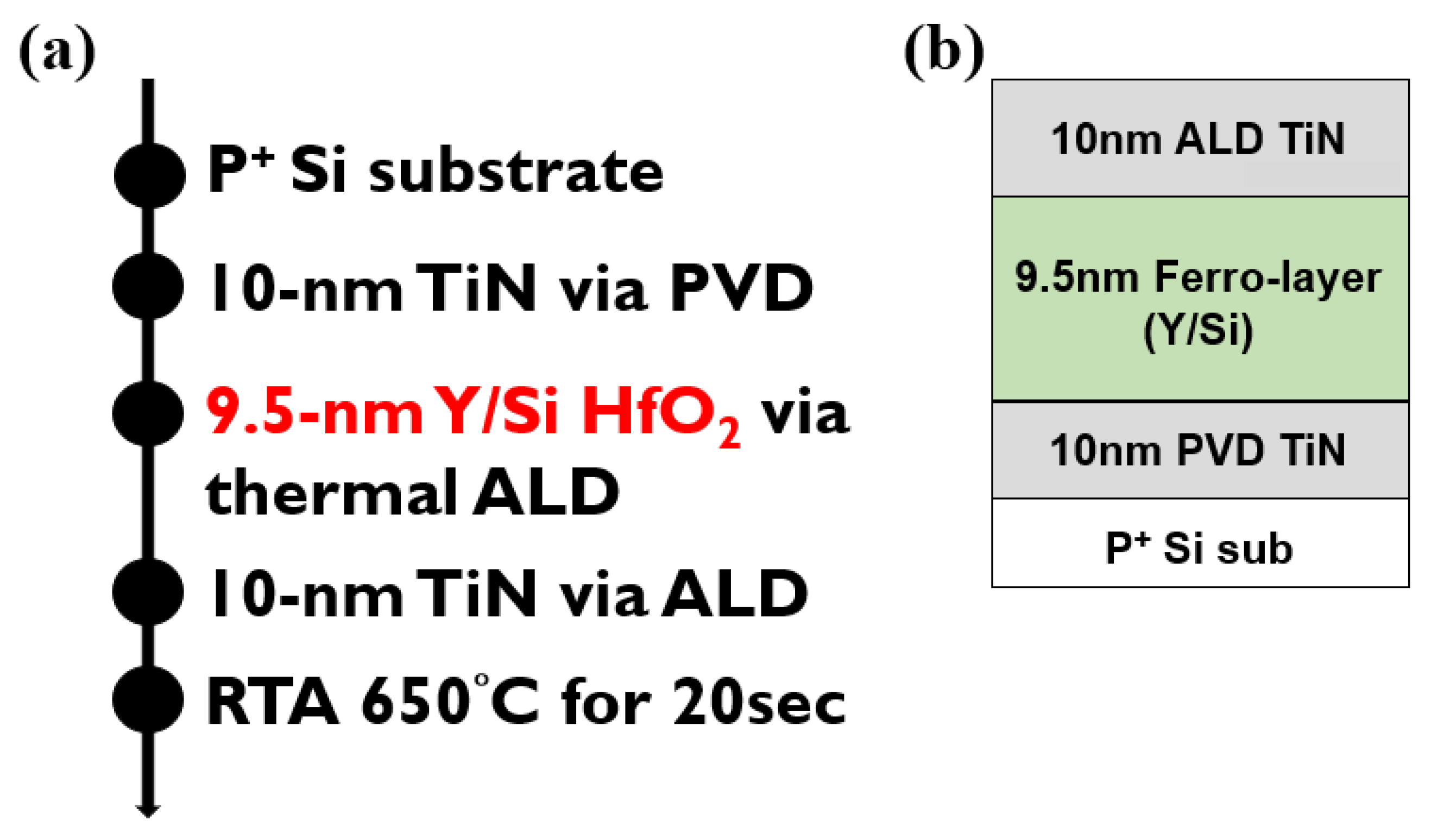
2. Materials and Methods
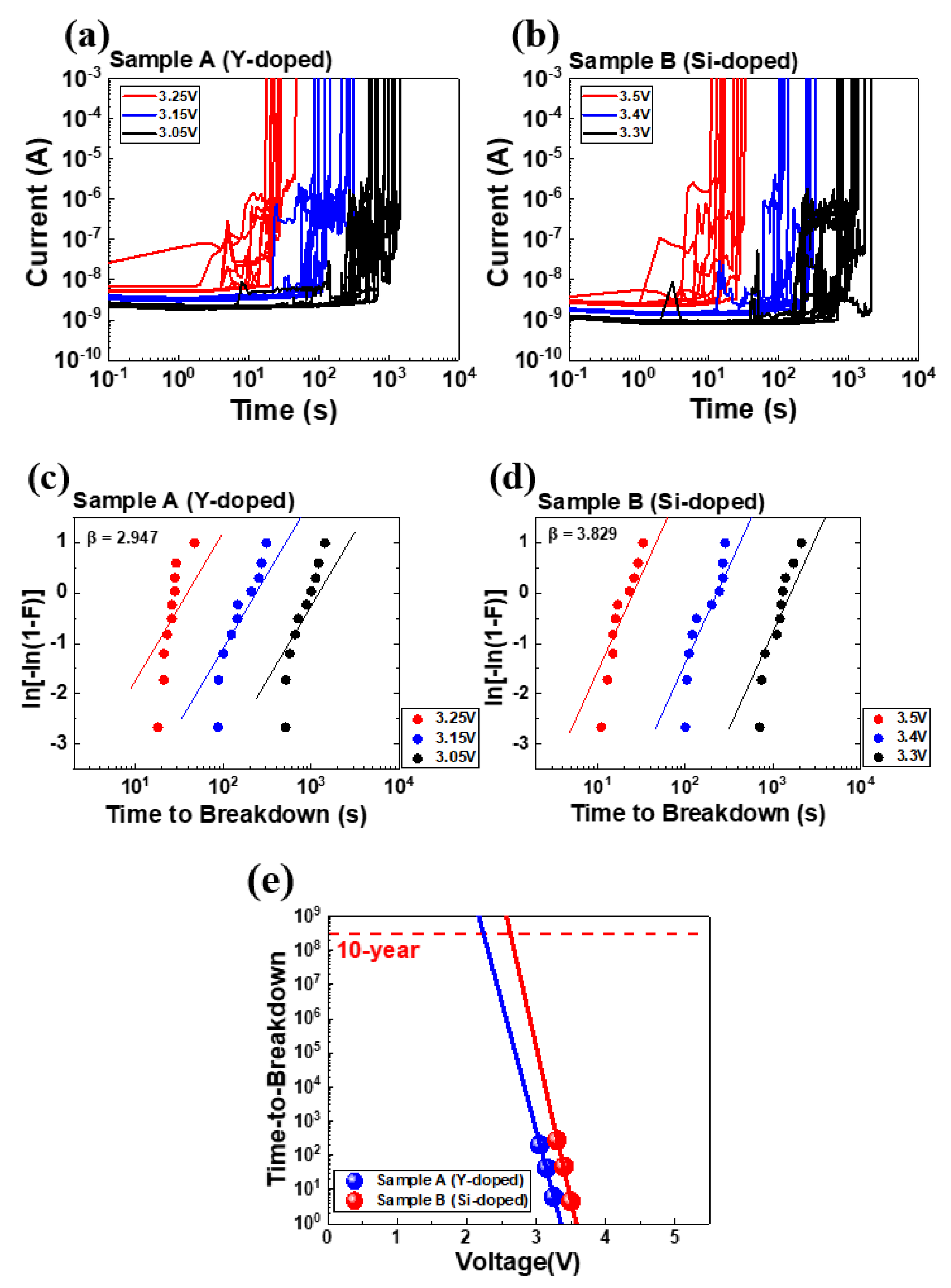
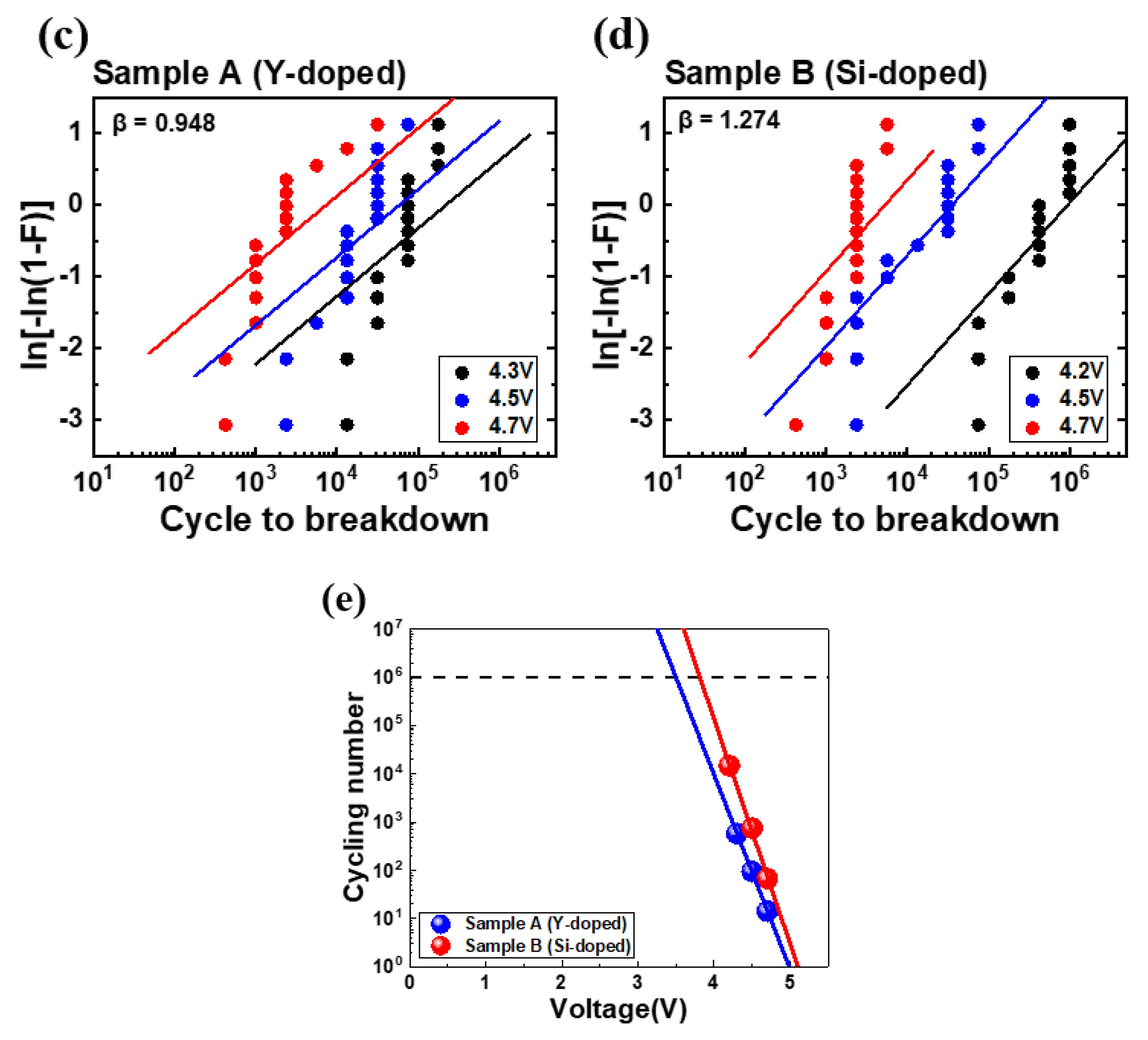
Figure 1 shows the schematic structure of metal-ferroelectric-metal (MFM) capacitors and a brief process flow of this work. At first, 10-nm TiN was deposited via PVD as the bottom electrode. Next, 9.5-nm HfO2-based ferroelectric layers with two different dopants, Y and Si, were deposited via thermal ALD at 300 °C. Afterward, another 10-nm TiN was deposited via ALD on the ferroelectric films as the top metal electrode. Lastly, RTA was conducted in N2 ambient at 650 °C for crystallization for 20 s.
The measurement setup for the capacitor used in this study was 2400 μm2 (60 μm × 80 μm). To perform electrical characterizations such as I-V (current-voltage) and time-dependent dielectric breakdown (TDDB) measurements, a Keysight B1500 Source Measurement Unit (SMU) Keysight, USA, was employed. To characterize the ferroelectric properties, including P-V (polarization-voltage) and cycle-to-breakdown measurements, a Keysight B1530 Waveform Generator/Function Measurement Unit (WGFMU) Keysight, USA, was utilized. In this setup, the capacitor was biased at the bottom via a chuck electrode, while a ground electrode was placed on top.
To compare the sample’s domain size, distribution, and homogeneity, we used contact resonance piezoresponse force microscopy (PFM). Although a quantitative interpretation of the results is beyond the scope of this work, we used the same probe. We also operated under the same conditions on two samples with the same physical thickness (9.5 nm). Therefore, the results represent a relative comparison between samples and can be used to analyze the domain size (Figure 2). For instance, Sample A (Y-doped) has a smaller domain size than Sample B (Si-doped). Details of the domain structures can also be found elsewhere [23]. Table 1 briefly describes the dopants and domain sizes used in this study. Distinct differences in the domain sizes of Sample A and Sample B can be used to understand the impact of domain size on the reliability of MFM devices.

3. Results

To understand ferroelectricity, we used P-V measurements with a triangular pulse of 10 μs/V and a trapezoidal plus with Tr (rising time)/Tf (falling time) fixed at 0.5 μs and Twidth (pulse width) set at 1μs for the cycling. Figure 3 shows the P-V characteristics of Samples A and B in the fresh state and after 103 cycles. Figure 4 shows comprehensive endurance characteristics at different cycling numbers. Sample A shows a slightly larger 2Pr than Sample B in the pristine state. Upon increasing the cycling number, Sample A exhibits a clear wake-up effect with a saturation of 2Pr after 104 cycles. However, Sample B does not exhibit a saturation of 2Pr. Overall, Sample A shows a larger 2Pr than Sample B after 105 cycles
To understand the impact of domain size on time-dependent breakdown stability, we performed constant voltage stress time-dependent dielectric breakdown and cycling-to-breakdown evaluations. Figure 5 and Figure 6 show the results of the constant voltage stress (CVS) time-dependent dielectric breakdown (TDDB) and cycle-to-breakdown evaluations in Samples A and B, respectively.
Figure 5c,d shows Weibull plots of time-to-breakdown (tBD) distributions for three TDDB VG conditions, which follow the Weibull failure distribution:
ln ln 1 F t = β ln t β ln η
where t is the time; β is the shape parameter; η is the scale factor of 63.2% value. The fitted β is 2.497 and 3.829 for Samples A and B, respectively. A higher β implies a tight distribution and small variability.
In Figure 5e, lifetime of 1% failure analyses are extrapolated from the Weibull plot of tBD distribution and projected to a 10-year line. The operating voltages of Sample A are slightly lower than Sample B (2.62 V) at 2.24 V.
In designing the cycle-to-breakdown (Cycle-to-BD) measurement, we chose a PUND waveform with triangular pulses for the reading state. We set the rising, falling, and delay times (Tr/Tf/Tdelay) to a fixed duration of 5 μs. The PUND waveform allowed for clear observation of whether or not the sample experienced breakdown. In the cycling state, trapezoidal pulses were used as the waveform. The Tr and Tf were fixed at 0.5 μs, while the Twidth was set to 1 μs. To determine the cycles of the chosen reading step, we divided the interval to reach 1E6 cycles into 12 segments. After calculations, we determined that 100.375 cycles would serve as the interval between the two consecutive reading states.
Similar to the TDDB analysis, cycle-to-breakdown (Cycle-to-BD) distributions for three different Cycle-to-BD VG conditions were used to construct Weibull plots. These plots were then used to extract fitting values from the ß value and generate lifetime curves. However, to adapt the Weibull failure distribution to the Cycle-to-BD analysis, the time-to-BD (tBD) was transformed into cycle-to-BD (CBD). Figure 6c,d display the fitting β values and corresponding lines for different devices. Sample A yielded a fitted β value of 0.948, while sample B had a βvalue of 1.274. These values are consistent with the TDDB analysis results, where Sample B exhibited a higher β value. The discrepancy in β values between TDDB and Cycle-to-BD measurements may be due to the Cycle-to-BD measurement using both positive and negative pulses during the cycling stage compared to TDDB measurements with a constant positive bias.
Figure 6e illustrates the 1% failure analysis of the 106-cycle lifetime analysis. The trend observed in the Cycle-to-BD analysis is similar to the TDDB analysis. For Sample A, the determined operating voltage is 3.45 V, which is slightly lower than Sample B’s operating voltage of 3.79 V.
Figure 7 shows the correlation between operation voltage (based on constant voltage stress TDDB and cycle-to-breakdown measurements) and domain size. Table 2 summarizes operation voltages based on CVS TDDB and cycle-to-breakdown evaluations. Figure 7 indicates that a larger domain size exhibits better TDDB and cycle-to-breakdown stability, i.e., higher 10-year operation voltages and higher voltages up to 106 cycles. In addition, Table 3 presents the maximum lifetime of targeting applied voltage at 3V results that Samples A and B can withstand in seconds. We calculated the lifetime of the Cycle-to-BD measurement by multiplying the predicted breakdown cycling number by a duration of 1 cycle in the measurement waveform design. According to our results, the lifetime measured in the TDDB analysis is longer than in the Cycle-to-BD analysis. This finding indicates that the measurement technique involving the continuous application of the same bias direction is less likely to induce defects generation and device breakdown than the technique involving a continuously changing bias direction. However, from the lifetimes in seconds, Sample B still exhibits a longer lifetime with a larger domain size in both the TDDB and Cycle-to-BD measurements. These findings are consistent with previous results.
The charging effects along the domain boundaries have been reported [24]. Therefore, larger domain sizes represent fewer domain boundaries (Figure 8) and reduce the chance of charging effects that create leakage paths as bias is applied to the device, thereby improving TDDB and cycle-to-breakdown stability. Besides, it is worth noting that Sample B exhibits larger β than Sample A, indicating better uniformity due to fewer domain boundaries in Sample B. In summary, larger domain sizes and fewer domain boundaries can improve CVS TDDB and cycle-to-breakdown reliability. However, samples with a larger domain size may degrade ferroelectricity.

4. Conclusions

In this study, the impact of domain size on the constant voltage stress TDDB and cycle-to-breakdown reliability are systematically reported. Firstly, MFM devices were fabricated with two different dopants in the ferroelectric layer, which intentionally induced different domain sizes. The PFM analysis indicated that Sample B (Si-doped) had a larger domain size than Sample A (Y-doped). Furthermore, CVS TDDB and cycle-to-breakdown evaluations were conducted in Sample A and Sample B, indicating that Sample B had better CVS TDDB and cycle-to-breakdown stability. A clear correlation was observed between the larger domain size and better time-dependent stability, which may be attributed to fewer domain boundaries in Sample B. We are the first to report the effects of domain size on CVS TDDB and cycle-to-breakdown reliability and conclude that optimizing the domain size can improve devices’ reliability.

Author Contributions

Conceptualization, T.-Y.C., K.-C.W. and T.-L.W.; methodology, T.-Y.C., K.-C.W. and T.-L.W.; formal analysis, T.-Y.C., K.-C.W., H.-Y.L., N.R., U.C. and T.-L.W.; investigation, T.-Y.C., K.-C.W., H.-Y.L., N.R., U.C. and T.-L.W.; data curation, T.-Y.C. and K.-C.W.; writing—original draft preparation, T.-Y.C. and T.-L.W.; writing—review and editing, J.-H.H., W.-C.P., N.R., U.C., K.B., J.V.H. and T.-L.W.; supervision, N.R. and T.-L.W.; project administration, N.R. and T.-L.W.; funding acquisition, T.-L.W. All authors have read and agreed to the published version of the manuscript.

Funding

This work was financially supported by the “Advanced Semiconductor Technology Research Center” from The Featured Areas Research Center Program within the framework of the Higher Education Sprout Project by the Ministry of Education (MOE) in Taiwan. This work was also partly supported by the Ministry of Science and Technology, Taiwan, under Grant MOST 111-2634-F-A49-008, 111-2622-8-A49-018-SB, and 112-2636-E-A49-005.

Institutional Review Board Statement

Not applicable.

Informed Consent Statement

Not applicable.

Data Availability Statement

The data presented in this study are available upon request from the corresponding author. The data are not publicly available due to privacy.

Acknowledgments

This work was financially supported by the “Advanced Semiconductor Technology Research Center” from The Featured Areas Research Center Program within the framework of the Higher Education Sprout Project by the Ministry of Education (MOE) in Taiwan. This work was also partly supported by the Ministry of Science and Technology, Taiwan, under Grant MOST 111-2634-F-A49-008, 111-2622-8-A49-018-SB, and 112-2636-E-A49-005.

Conflicts of Interest

The authors declare no conflict of interest.

References

  1. Böscke, T.S.; Müller, J.; Bräuhaus, D.; Schröder, U.; Böttger, U. Ferroelectricity in hafnium oxide thin films. Appl. Phys. Lett. 2011, 99, 102903. [Google Scholar] [CrossRef]
  2. Song, C.M.; Kwon, H.J. Ferroelectrics based on HfO2 film. Electronics 2021, 10, 2759. [Google Scholar] [CrossRef]
  3. Müller, J.; Böscke, T.S.; Schröder, U.; Mueller, S.; Bräuhaus, D.; Böttger, U.; Frey, L.; Mikolajick, T. Ferroelectricity in Simple Binary ZrO2 and HfO2. Nano Lett. 2012, 12, 4318–4323. [Google Scholar] [CrossRef] [PubMed]
  4. Cheema, S.S.; Kwon, D.; Shanker, N.; Reis, R.D.; Hsu, S.-L.; Xiao, J.; Zhang, H.; Wagner, R.; Datar, A.; McCarter, M.R.; et al. Enhanced ferroelectricity in ultrathin films grown directly on silicon. Nature 2020, 580, 478–482. [Google Scholar] [CrossRef] [PubMed]
  5. Banerjee, W. Challenges and Applications of Emerging Nonvolatile Memory Devices. Electronics 2020, 9, 1029. [Google Scholar] [CrossRef]
  6. Salahuddin, S.; Datta, S. Use of negative capacitance to provide voltage amplification for low power nanoscale devices. Nano Lett. 2008, 8, 405–410. [Google Scholar] [CrossRef] [PubMed]
  7. Chou, C.-P.; Lin, Y.-X.; Huang, Y.-K.; Chan, C.-Y.; Wu, Y.-H. Junctionless Poly-GeSn Ferroelectric Thin-Film Transistors with Improved Reliability by Interface Engineering for Neuromorphic Computing. ACS Appl. Mater. Interfaces 2019, 12, 1014–1023. [Google Scholar] [CrossRef] [PubMed]
  8. MKim, M.K.; Lee, J.S. Ferroelectric analog synaptic transistors. Nano Lett. 2019, 19, 2044–2050. [Google Scholar] [CrossRef]
  9. Jerry, M.; Chen, P.Y.; Zhang, J.; Sharma, P.; Ni, K.; Yu, S.; Datta, S. Ferroelectric FET analog synapse for acceleration of deep neural network training. In Proceedings of the 2017 IEEE International Electron Devices Meeting (IEDM), San Francisco, CA, USA, 2–6 December 2017; pp. 6.2.1–6.2.4. [Google Scholar] [CrossRef]
  10. Kimura, H.; Hanyu, T.; Kameyama, M.; Fujimori, Y.; Nakamura, T.; Takasu, H. Complementary ferroelectric-capacitor logic for low-power logic-in-memory VLSI. IEEE J. Solid-State Circuits 2004, 39, 919–926. [Google Scholar] [CrossRef]
  11. Wang, Y.Y.; Wang, K.C.; Wu, C.H.; Chang, T.Y.; Ronchi, N.; Banerjee, K.; Van den Bosch, G.; Van Houdt, J.; Wu, T.L. Demonstration of 64 Conductance States and Large Dynamic Range in Si-doped HfO2 FeFETs under Neuromorphic Computing Operations. In Proceedings of the 2022 International Symposium on VLSI Technology, Systems and Applications (VLSI-TSA), Hsinchu, Taiwan, 18–21 April 2022; pp. 1–2. [Google Scholar] [CrossRef]
  12. Chen, Y.H.; Su, C.J.; Hu, C.; Wu, T.L. Effects of Annealing on Ferroelectric Hafnium Zirconium Oxide-Based Transistor Technology. IEEE Electron Device Lett. 2019, 40, 467–470. [Google Scholar] [CrossRef]
  13. Cao, R.; Wang, Y.; Zhao, S.; Yang, Y.; Zhao, X.; Wang, W.; Zhang, X.; Lv, H.; Liu, Q.; Liu, M. Effects of Capping Electrode on Ferroelectric Properties of Hf0.5Zr0.5O2 Thin Films. IEEE Electron Device Lett. 2018, 39, 1207–1210. [Google Scholar] [CrossRef]
  14. Ronchi, N.; Ragnarsson, L.Å.; Breuil, L.; Banerjee, K.; McMitchell, S.R.C.; O’Sullivan, B.; Milenin, A.; Kundu, S.; Pak, M.; Van Houdt, J. Ferroelectric FET with Gd-doped HfO2: A Step Towards Better Uniformity and Improved Memory Performance. In Proceedings of the 2021 Silicon Nanoelectronics Workshop (SNW), Kyoto, Japan, 13 June 2021; pp. 1–2. [Google Scholar]
  15. Skopina, E.V.; Guillaume, N.; Alrifai, L.; Gonon, P.; Bsiesya, A. Sub-10-nm ferroelectric Gd-doped HfO2 layers. Appl. Phys. Lett. 2022, 120, 172901. [Google Scholar] [CrossRef]
  16. Tashiro, Y.; Shimizu, T.; Mimura, T.; Funakubo, H. Comprehensive Study on the Kinetic Formation of the Orthorhombic Ferroelectric Phase in Epitaxial Y-Doped Ferroelectric HfO2 Thin Films. ACS Appl. Electron. Mater. 2021, 3, 3123–3130. [Google Scholar] [CrossRef]
  17. Li, S.; Zhou, D.; Shi, Z.; Hoffmann, M.; Mikolajick, T.; Schroeder, U. Temperature-Dependent Subcycling Behavior of Si-Doped HfO2 Ferroelectric Thin Films. ACS Appl. Electron. Mater. 2021, 3, 2415–2422. [Google Scholar] [CrossRef]
  18. Wu, C.-H.; Wang, K.-C.; Wang, Y.-Y.; Hu, C.; Su, C.-J.; Wu, T.-L. Enhancement of Ferroelectricity in 5 nm Metal-Ferroelectric -Insulator Technologies by Using a Strained TiN Electrode. Nanomaterials 2022, 12, 468. [Google Scholar] [CrossRef]
  19. Wu, C.-H.; Ronchi, N.; Wang, K.-C.; Wang, Y.-Y.; McMitchel, S.; Banerjee, K.; Van den Bosch, G.; Van Houdt, J.; Wu, T.-L. Impacts of Pulsing Schemes on the Endurance of Ferroelectric Metal–Ferroelectric–Insulator–Semiconductor Capacitors. IEEE J. Electron Devices Soc. 2022, 10, 109–114. [Google Scholar] [CrossRef]
  20. Popovici, M.I.; Bizindavyi, J.; Favia, P.; Clima, S.; Alam, M.N.K.; Ramachandran, R.K.; Walke, A.M.; Celano, U.; Leonhardt, A.; Mukherjee, S.; et al. High performance La-doped HZO based ferroelectric capacitors by interfacial engineering. In Proceedings of the 2022 International Electron Devices Meeting (IEDM), San Francisco, CA, USA, 3–7 December 2022. [Google Scholar]
  21. Tan, A.J.; Liao, Y.-H.; Wang, L.-C.; Shanker, N.; Bae, J.-H.; Hu, C.; Salahuddin, S. Ferroelectric HfO2 Memory Transistors with High-κ Interfacial Layer and Write Endurance Exceeding 1010 Cycles. IEEE Electron Device Lett. 2021, 42, 994–997. [Google Scholar] [CrossRef]
  22. Zagni, N.; Puglisi, F.M.; Pavan, P.; Alam, M.A. Reliability of HfO2-Based Ferroelectric FETs: A Critical Review of Current and Future Challenges. Proc. IEEE 2023, 111, 158–184. [Google Scholar] [CrossRef]
  23. Ronchi, N.; Ragnarsson, L.Å.; Celano, U.; Kaczer, B.; Kaczmarek, K.; Banerjee, K.; McMitchell, S.R.C.; Van Houdt, J. A comprehensive variability study of doped HfO2 FeFET for memory applications. In Proceedings of the 2022 IEEE International Memory Workshop (IMW), Dresden, Germany, 15–18 May 2022. [Google Scholar]
  24. Wei, X.K.; Sluka, T.; Fraygola, B.; Feigl, L.; Du, H.; Jin, L.; Setter, N. Controlled charging of ferroelastic domain walls in oxide ferroelectrics. ACS Appl. Mater. Interfaces 2017, 9, 6539–6546. [Google Scholar] [CrossRef] [PubMed]
Figure 1. (a) Schematic of the process flow and (b) schematic structure of MFM capacitors with different dopants in ferroelectric layers.
Nanomaterials 13 02104 g001
Figure 2. Contact resonance piezoresponse force microscopy PFM measurements in Sample A (Y-doped) and Sample B (Si-doped).
Nanomaterials 13 02104 g002
Figure 3. P-V characteristics in Samples A and B.
Nanomaterials 13 02104 g003
Figure 4. Polarization characteristics with respect to cycling numbers.
Nanomaterials 13 02104 g004
Figure 5. Gate current for (a) Sample A and (b) Sample B, as monitored by six different voltages (10 devices per group). (c,d) show corresponding Weibull plots of tBD. (e) Operating voltage extrapolation for a 10-year lifetime at 1% failure for devices with Samples A and B.
Nanomaterials 13 02104 g005
Figure 6. 2Pr for (a) Sample A and (b) Sample B, as monitored by six different voltages (10 devices per group). (c,d) show corresponding Weibull plots of cycle-to-breakdown. (e) Operating cycling number extrapolation for a 106-cycling lifetime at 1% failure for Samples A and B.
Nanomaterials 13 02104 g006aNanomaterials 13 02104 g006b
Figure 7. Extrapolated voltages vs. domain size under CVS TDDB (a) and cycle-to-breakdown measurements (b).
Nanomaterials 13 02104 g007
Figure 8. Schematic illustration of domain size’s effect on the leakage path.
Nanomaterials 13 02104 g008
Table 1. A brief summary of the dopants and domain sizes used in this study.
Dopant in
Ferroelectric Layer
Domain Size
(nm)
Doping
Concentration
Sample AY5.62.9%
Sample BSi12.52.5%
Table 2. Summary of the extrapolated operation voltage.
10-year
Operation
Voltage Based
on CVS TDDB
106-Cycling
Operation
Voltage Based on
Cycle-to-Breakdown
Sample A2.243.45
Sample B2.623.79
Table 3. The maximum lifetime results that two samples can withstand in seconds.
Lifetime
of Cycle-to-BD @3V
(s)
Lifetime
of TDDB @3V
(s)
Sample A203 515
Sample B12,170 146,058
Disclaimer/Publisher’s Note: The statements, opinions and data contained in all publications are solely those of the individual author(s) and contributor(s) and not of MDPI and/or the editor(s). MDPI and/or the editor(s) disclaim responsibility for any injury to people or property resulting from any ideas, methods, instructions or products referred to in the content.

