Article

Improved Electrical Properties of EHD Jet-Patterned MoS2 Thin-Film Transistors with Printed Ag Electrodes on a High-k Dielectric

School of Electronics and Display Engineering, Hoseo University, Asan 31499, Republic of Korea
*
Author to whom correspondence should be addressed.
Current address: Faculty of Physics, Hanoi National University of Education, Hanoi 100000, Vietnam.
Nanomaterials 2023, 13(1), 194; https://doi.org/10.3390/nano13010194
Submission received: 20 November 2022 / Revised: 28 December 2022 / Accepted: 28 December 2022 / Published: 1 January 2023
(This article belongs to the Special Issue 2D Semiconducting Materials for Device Applications)

Abstract

:
Electrohydrodynamic (EHD) jet printing is known as a versatile method to print a wide viscosity range of materials that are impossible to print by conventional inkjet printing. Hence, with the understanding of the benefits of EHD jet printing, solution-based MoS2 and a high-viscosity Ag paste were EHD jet-printed for electronic applications in this work. In particular, printed MoS2 TFTs with a patterned Ag source and drain were successfully fabricated with low-k silica (SiO2) and high-k alumina (Al2O3) gate dielectrics, respectively. Eventually, the devices based on Al2O3 exhibited much better electrical properties compared to the ones based on SiO2. Interestingly, an improvement of around one order of magnitude in hysteresis was achieved for devices after changing the gate insulator from SiO2 to Al2O3. In effect, the results of this work for the printed MoS2 and the printed Ag source and drains for TFTs demonstrate a new approach for jet printing in the fabrication of electronic devices.

1. Introduction

Graphene, the first material in the two-dimensional (2D) family of materials, has been used in a large number of scientific applications due to its superior and novel properties, e.g., mechanical, thermal, electrical, optical, etc. [1]. Likewise, as an emerging candidate in the crowd of 2D materials, transition metal dichalcogenides (TMDs) have drawn much attention due to their sizeable bandgap, which is definitely better than the unfavorable zero bandgap of graphene [2]. In particular, molybdenum disulfide (MoS2) is one of the most studied TMDs, with diverse applications [3,4] because of its tremendously high intrinsic electron mobility and indirect-to-direct bandgap from 1.2 eV in bulk to 2.0 eV in the monolayer—especially in thin-film transistor device applications [5].
Researchers have devoted considerable efforts to synthesizing high-quality MoS2 with a controllable number of layers, playing a significant role in the fundamental research and application explorations involving this material. Generally, a variety of methods have been proposed to produce 2D TMD materials, including mechanical/chemical exfoliation [6,7], chemical vapor deposition (CVD) [8], wet-chemical based methods [9], and so on. Even though the growth of atomically thin TMD films via the CVD method is one of the most popular ways of producing these films, controlling the respective concentrations of the precursors precisely during the growth process is still challenging. Next, exfoliation methods, despite their simple and low-cost features, face the issue of random shape/thickness of the resulting films from the mechanical strategy and the diminished semiconductor properties of the films. Therefore, they are unsuitable for the production of 2D TMD materials for large areas over wafer-scale and high-throughput applications. In this context, the wet-chemical-based method seems to be the method of choice for synthesizing high-quality MoS2 with a controllable number of layers in a relatively simple and easy way.
In the solution method, reports of jet-printed MoS2-based TFTs with printed source and drain (S/D) electrodes are still rare. So far, there have been several metal nanoparticle pastes that can be printed, such as nanoparticle pastes of Au, Al, Cu, Ag, etc. Additionally, gold is a highly conductive material, but its prohibitive price is disadvantageous for use in mass production of TFTS. In contrast, aluminum and copper are preferred because of their low price and good conductivity, but they are easily oxidized in the atmosphere, resulting in the degradation of their electrical features. Meanwhile, silver shows many outstanding merits, such as having the highest electrical conductivity among the materials that can be printed, along with its chemical stability and affordable price, making Ag stand out from the other materials. The undeniable possibility of using patterned Ag for electrodes in TFT devices fabricated by EHD jet printing was confirmed by our previous research [10]. In this previous work, the sheet resistance of printed Ag was evaluated to be around 0.027 Ω−1—comparable or even superior to that of Ag layers made by other methods, such as inkjet printing and screen printing [11,12]. Hence, we chose high-viscosity Ag paste for patterning the source and drain for the TFTs in this work.
The improvement of TFTs’ characteristics by using a high-k dielectric has been studied previously [13]. However, the use of an Al2O3 dielectric layer in solution-based MoS2 TFTs with printed Ag S/D contacts—especially in a back-gated configuration—has not been explored to date. Hence, this work presents the advantages of EHD jet-printing technology in patterning electrical elements from various viscous materials and investigates the properties of high-k dielectric-based solution-processed MoS2 TFTs (Figure 1). This work demonstrates the suitability of direct EHD jet-printing technology for mass production of TFTs because of its low cost and high performance.

2. Experimental Details

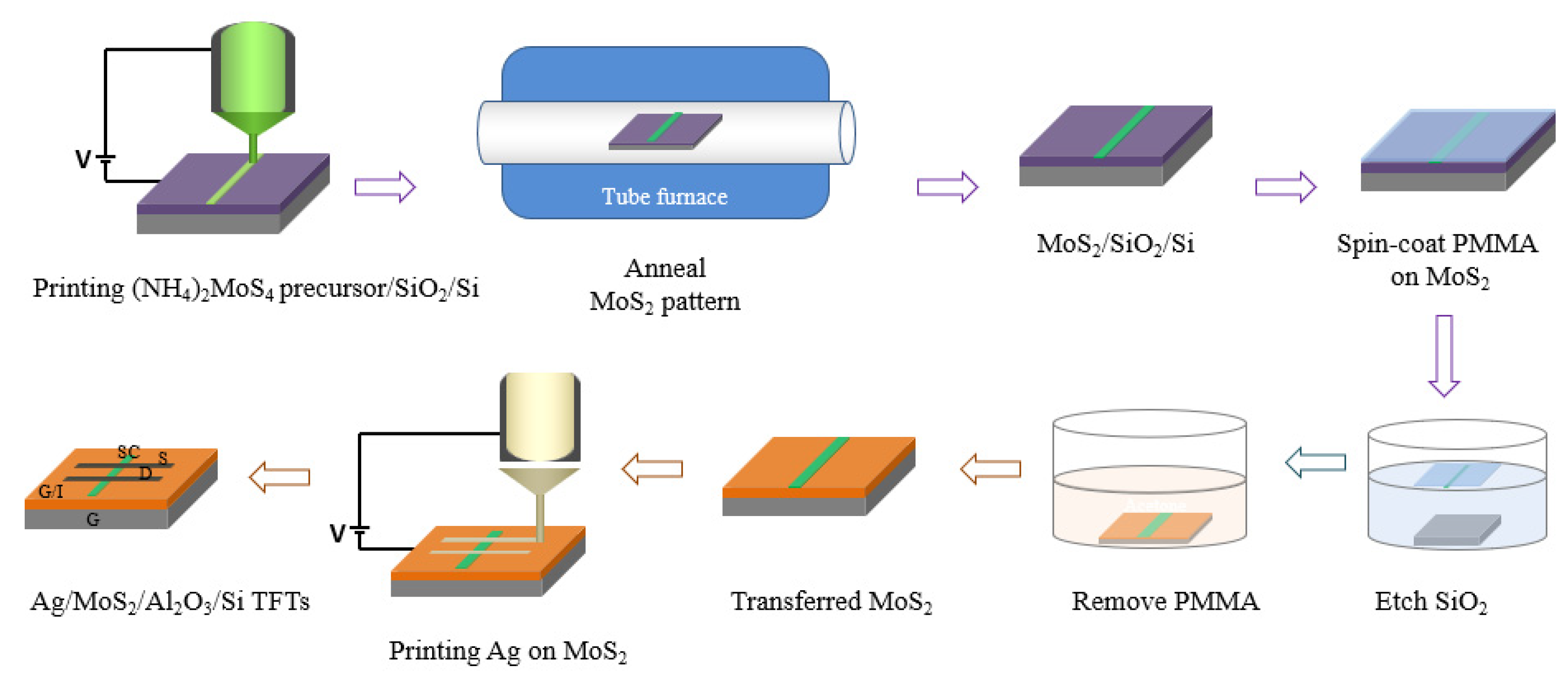
2.1. Growth of MoS2 Layers

MoS2 patterns were created by a combination of EHD jet printing and one-step annealing following the process described in our previous research [9]. First, the ammonium tetrathiomolybdate ((NH4)2MoS4) precursor solution for printing was prepared with concentrations of 25, 50, 75, and 100 m M by stirring the (NH4)2MoS4 in a group of solvents of ethanolamine and butylamine for 12 h. Subsequently, a S-rich solution was formed by preparing a 1 M sulfur solution with carbon disulfide (CS2) and dissolving the sulfur solution in the (NH4)2MoS4 precursor solution with N,N-dimethylformamide. All chemicals used in this formulation were purchased from Sigma-Aldrich (Milwaukee, WI, USA) and ThermoFisher (Fisher Scientific, Leicestershire, UK) and used without further purification.
For the printing of (NH4)2MoS4 on a UV/O3-irradiated 300 nm thick SiO2/Si substrate, the as-prepared precursor solution was collected in a syringe pump connected to a vertically movable plastic tip. The target substrate was then placed stably on a metal stage that could be moved on a horizontal plane, as described in our previous report [10]. Subsequently, for patterning the (NH4)2MoS4 lines, the voltage was adjusted to stretch the meniscus of the solution at the tip’s mouth into an upside-down cone shape, called the Taylor cone-jet mode. In particular, the printing parameters for patterning the (NH4)2MoS4 lines were a tip height of 2 mm, an applied voltage of 1.8–1.9 kV, a substrate temperature of 50 °C, a solution flow rate of 0.0032 μ L s−1, and a stage speed range of 2000–8000 μ m s−1. After printing the line patterns from the S-rich (NH4)2MoS4 solution, the patterns were pre-annealed at 150 °C for 20 min in ambient air using a hot plate. The pre-annealed patterns were then moved into a tube furnace for their annealing at a high temperature of 1000 °C for 1 h in a low vacuum (10−1–10−2 Torr), without sulfurization or further post-annealing, resulting in the final crystalline MoS2 line patterns.

2.2. Transfer of MoS2 onto Other Substrates

The printed MoS2 on the SiO2/Si substrate, after annealing, was covered with a PMMA (avg. Mol wt. ~350,000 g mol−1 and ~996,000 g mol−1) layer using spin-coating (at a spinning speed of 3000 rpm for 30 s). The spin-coated sample was then baked at 200 °C for 2 h on a hot plate in ambient air. Subsequently, the PMMA/MoS2/SiO2/Si wafer was placed on the surface of an etchant mixture (HF:BOE:DI water (1:1:1)) to remove the SiO2. The resulting PMMA/MoS2 membrane was then cleaned from the etchant solution using deionized (DI) water. After discarding the etchant contaminant, the PMMA/MoS2 double layer was picked up on different target substrates for different purposes—for example, on Al2O3/Si for TFT fabrication, or on a Cu grid for transmission electron microscopy (TEM, Ultra-Corrected-Energy-Filtered -TEM Libra 200 HT Mc Cs) studies. Finally, the top PMMA layer was removed using acetone at 80 °C to obtain the patterned MoS2.

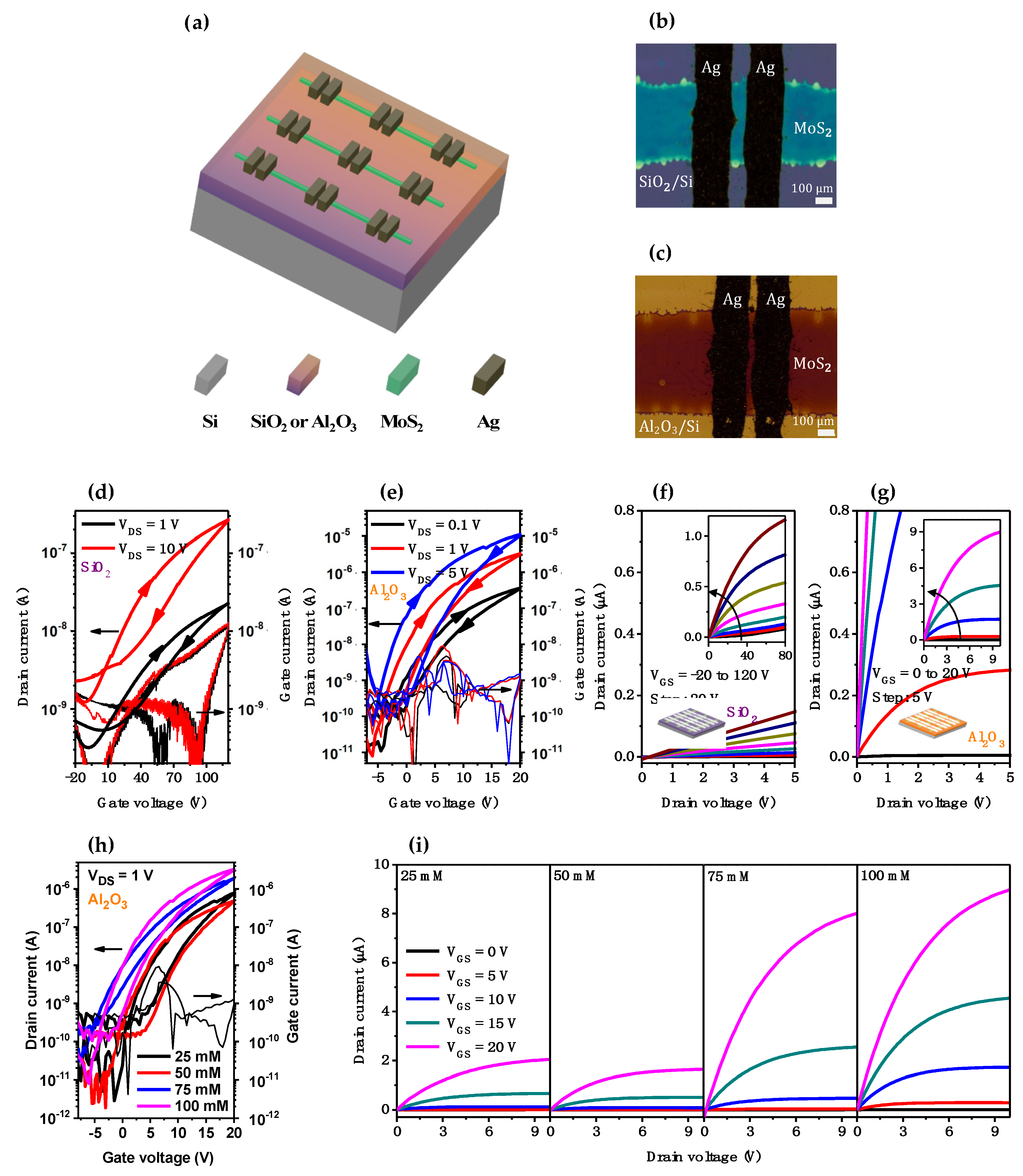
2.3. Device Fabrication

Printed TFTs were fabricated by EHD jet printing with MoS2 line patterns as the semiconductor layer and Ag line patterns as S/D electrodes in each TFT. For a bottom gate and top contact (BGTC) configuration of the TFT, first, 40 nm thick alumina was deposited by atomic layer deposition (ALD) on clean bare Si wafers. The as-grown/printed MoS2 was then transferred carefully from the SiO2/Si substrate onto a cleansed Al2O3/Si substrate using the above procedure involving PMMA. Notably, the smooth morphological surface of the MoS2 transferred onto other substrates was shown using an atomic force microscope (AFM, Nano expert II EM4SYS) to have no wrinkles or damage [14]. Finally, linear Ag patterns/terminals were printed perpendicularly on the MoS2 line patterns with the assistance of the pneumatic pressure due to the high viscosity of Ag. In particular, the silver line patterns were successfully EHD-printed with a tip–substrate gap of 1.5 mm, applied voltage of 1 kV, stage speed of 2000–2500 μ m s−1, and pressure of 80 kPa, and they were sintered at 200 °C for 30 min in ambient air. The whole fabrication process, from the preparation of the MoS2 line patterns to their transfer and the fabrication of the TFT devices, is sketched out in Figure 1.

3. Results and Discussion

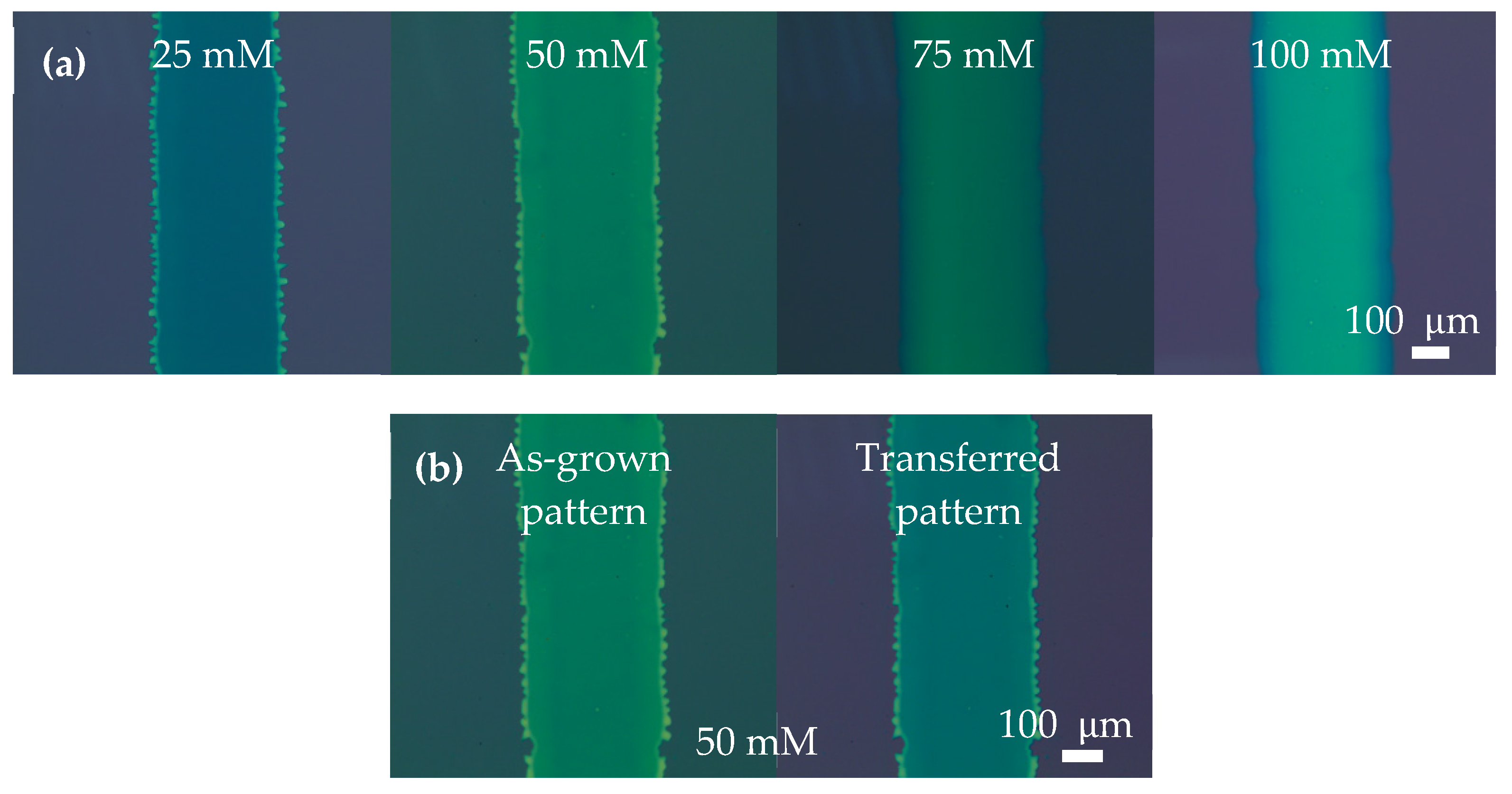
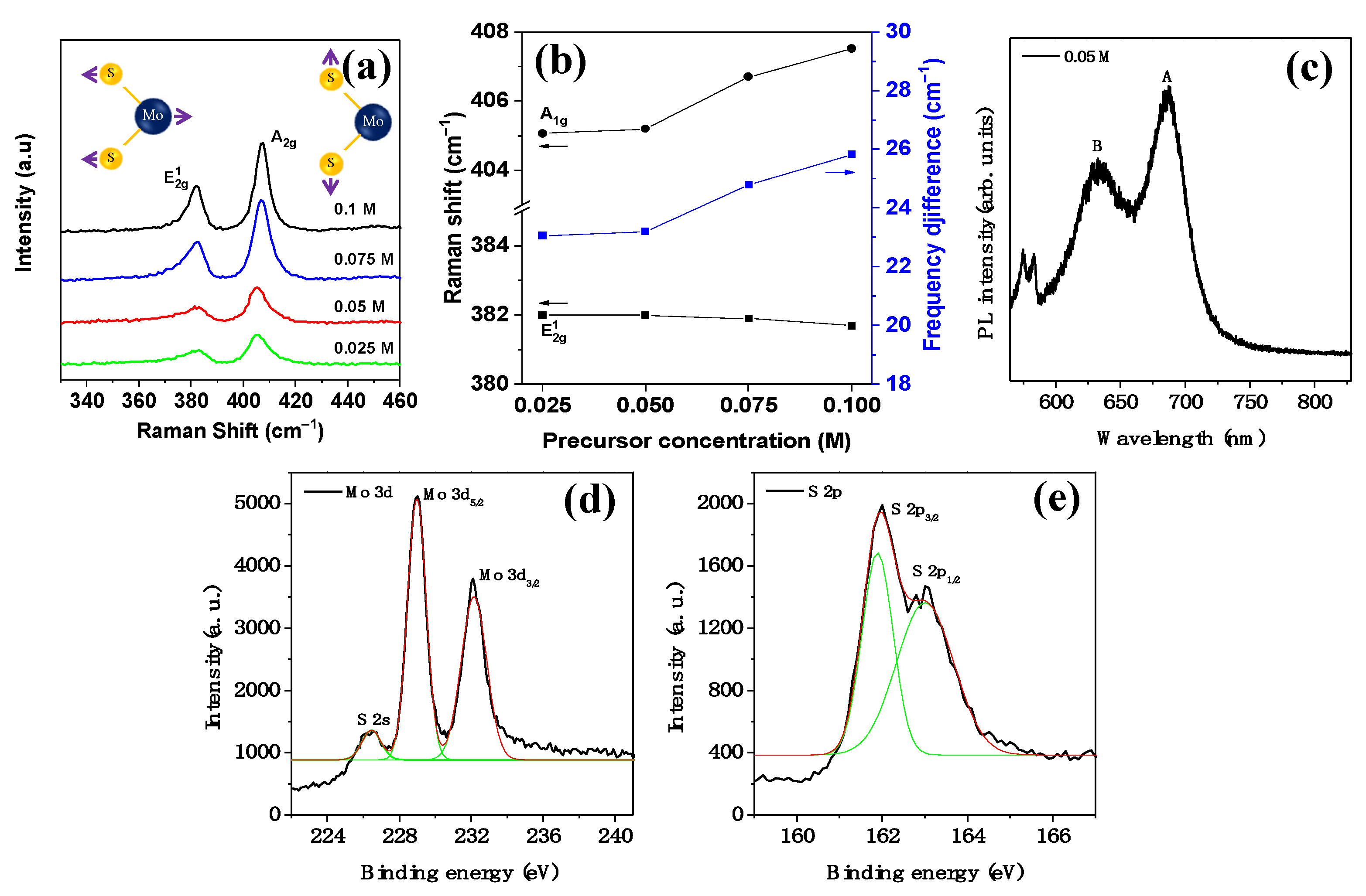
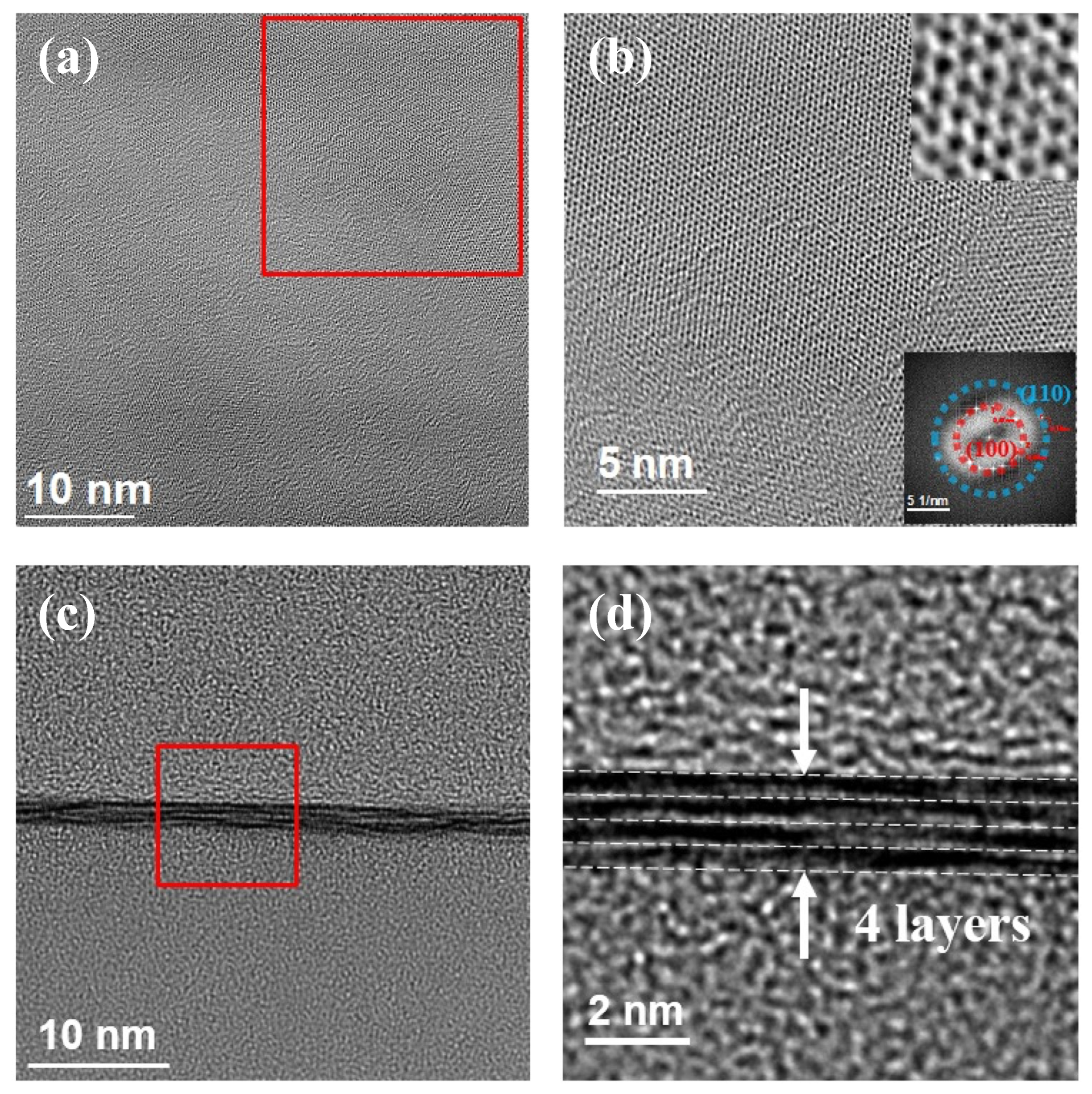
3.1. Printed MoS2 Line Patterns

Figure 2a shows the microscopic images of the MoS2 line patterns prepared with different (NH4)2MoS4 precursor concentrations using EHD jet printing. Visually, from left to right in this figure, the printed line patterns originating from increasing solution concentrations possess different thicknesses, which could be predicted from the color of the patterns. Moreover, all patterns showed smooth surfaces that were hole-free regardless of the concentrations (from 25 to 100 mM), demonstrating the printability and appropriately chosen concentration of the precursor solution. In addition, based on Figure 2b, the MoS2 pattern was proven to be undamaged and without wrinkles after transferring it using the PMMA-assisted method. Therefore, it is guaranteed that the MoS2 quality will be unchanged when the MoS2 is transferred to an arbitrary substrate to be used in further device fabrication.
For the evaluation of the composition and thickness of the printed MoS2, three methods of analysis—Raman, photoluminescence (PL), and XPS spectroscopies—were carried out on the printed MoS2. In particular, Raman spectroscopy was carried out under four different precursor solutions, from 25 to 100 m M. As shown in Figure 3a, two strong signals for the E 2 g 1 (at around 380 cm−1) and A 1 g (at around 405 cm−1) modes emerged in the Raman spectra regardless of the molar concentrations of the precursor solution. These two major modes assigned to the in-plane vibration of the Mo and S atoms and the out-of-plane vibration of the S atoms provided good evidence for the presence of the 2H phase of MoS2. It was also found that the two modes exhibited a well-defined concentration dependence, with the modes shifting opposite to one another with increasing concentration. Indeed, as the concentration was increased from 25 to 100 mM, the frequency difference between the modes increased gradually from 23.07 to 25.82 cm−1 (Figure 3b). Moreover, the Raman spectra suggested that the MoS2 line patterns obtained from concentrations of 25 mM and higher each consisted of at least three or four layers. Figure 3c describes the PL spectra of a representative MoS2 sample printed from the 50 mM precursor solution. Two specific peaks at about 686 and 632 nm in the spectra were attributed to the A1 and B1 excitons originating from the transition at the K-point of the Brillouin zone in the sample material, respectively.
The chemical composition of the printed MoS2 was determined by XPS. Figure 3d,e show the Mo 3d and S 2p regions, respectively, for the MoS2 that was printed from the 50 m M precursor solution and annealed. The Mo 3d XPS spectra were clearly observed to have two distinct peaks at 229.0 and 232.1 eV and a weak peak at 226.4 eV corresponding to the 3d5/2 and 3d3/2 of Mo4+ and S 2s, respectively. These peaks proved the presence of the 2H phase in MoS2. In addition, the peaks observed at 162.1 and 163.4 eV belonged to the divalent sulfide ions (S2−) 2p3/2 and 2p1/2 in 2H-MoS2, respectively.
Furthermore, typical nanoscale images of the MoS2 line pattern printed from the 25 mM concentration precursor solution were captured by TEM to observe the plane-view and thickness of the pattern. Figure 4a,b show the morphological TEM images of the printed line pattern at low and high resolutions of the TEM, respectively, revealing the honeycomb MoS2 surface. Moreover, this feature can be clearly seen in the top insert of Figure 4b. Furthermore, the fast Fourier transform (FFT) corresponding to the lower insert of Figure 4b depicts the polycrystallization of the printed MoS2. The layer number of the line pattern was found to be four monolayers from the cross-sectional view of the TEM image (Figure 4c). Meanwhile, the selected area of Figure 4c, magnified to the scale shown in Figure 4d, corresponded to the tetra-layer of the pattern.

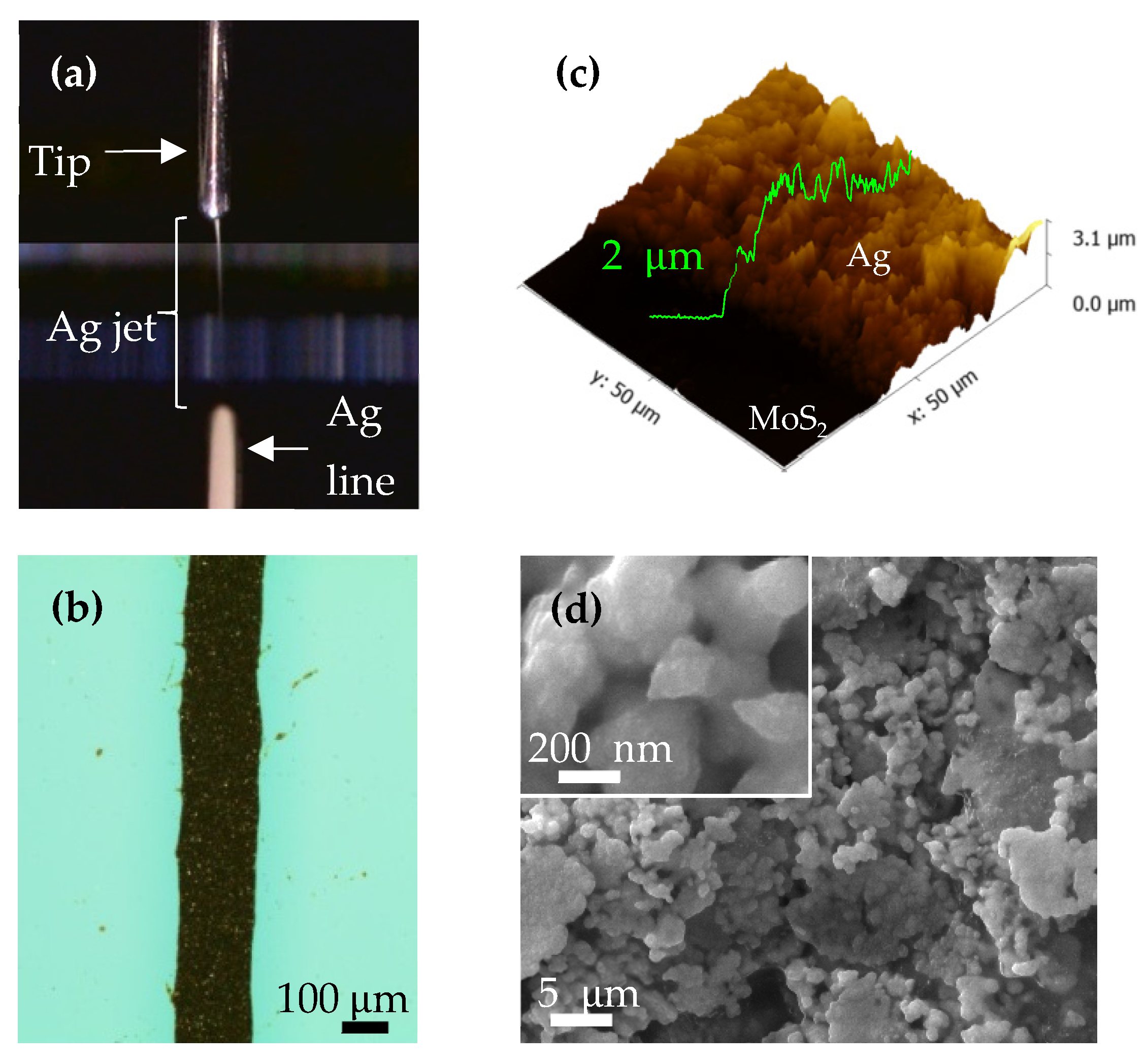
3.2. Printed Ag Line Patterns

The printing process of the Ag line patterns, illustrated in Figure 5a, clearly shows that the Taylor cone-jet mode was used to print the pattern. The width and clear shape of the Ag line patterns were found to be strongly dependent on the printing parameters—such as pressure, additive existence, and especially the stage speed—in our previous research [10]. Here, Figure 5b shows a typical microscope image of a Ag line pattern printed under the optimized conditions previously mentioned in the experimental section. The patterns were each observed to be 100–200 μ m in width, without serrated edges. Figure 5c shows the AFM height step image of the printed Ag line pattern on MoS2, and the thickness of the pattern was measured to be 2 μ m. Finally, according to the SEM image of the printed Ag line pattern after sintering, as shown in Figure 5d, although a rough morphology of the pattern was seen in the image, the distribution of the Ag particles was found to cover the entire substrate surface.

3.3. Printed MoS2 TFTs

The electrical properties of the printed MoS2 were characterized in a thin-film transistor application in which the integration of an ALD 40 nm Al2O3 dielectric, a printed MoS2 line pattern as a semiconductor, and printed Ag line patterns as top contacts was carried out. In this study, a counterpart TFT based on low-k SiO2 was also fabricated for comparison with the aforementioned high-k Al2O3-based TFT. Figure 6a shows the schematic of the BGTC MoS2 TFTs. Additionally, the top-view optical images of two typical TFTs, in which MoS2 was grown on SiO2 (k = 3.9) and transferred onto Al2O3 (k = 7.0), respectively, are shown in Figure 6b,c, respectively.
The field-effect mobility (μ) and threshold voltage ( V TH ) were calculated in the linear regime at a drain voltage ( V DS ) of 1 V for the TFT. The threshold voltage is defined as the intersection point of the V GS axis and the extrapolation of the linear region of the transfer curve. The linear field-effect mobility from each device was then calculated from the gradient of the drain current versus the gate voltage according to the following equation:
μ = L WCV DS × dI DS dV GS   V DS = 1   V
where L and W are the patterned MoS2 channel length and width, respectively, and C is the capacitance per unit area of the gate insulator. The length and width of the patterned MoS2 channel were about 40–100 and 500–600 μm (for various devices), respectively, used for calculating the TFTs’ performance in relation to the precursor concentrations and the dielectric layers, respectively.
For the primary evaluation of the TFTs, two TFT device groups with different dielectrics of Al2O3 (15.5 × 10⁻⁸ F cm−2) and SiO2 (10−8 F cm−2) were prepared from the same 100 mM MoS2 precursor solution. The I DS V GS transfer curves of these MoS2 devices are shown in Figure 6d,e. Due to the dissimilar materials and thicknesses of the dielectric layer, the applied voltage range should be different to prevent the breakdown of the devices. While sweeping V GS from −20 to 120 V (and back) at various constant V DS   values of at least 1 V for the 300 nm SiO2 TFT (Figure 6d), those for 40 nm Al2O3 were measured at about −10 V to 20 V (then back) and 0.1 V (Figure 6e), respectively. Notably, both TFT device types showed a clockwise hysteretic phenomenon associated with the electron trap at the MoS2–dielectric and/or MoS2–Ag interfaces. However, a dramatic reduction in hysteresis of one order of magnitude was achieved when using Al2O3 instead of SiO2 in the TFT, revealing smaller trap charges at the interface between MoS2 and Al2O3. In addition, although the maximum gate leakage current was about 10−9–10−8 A for the low- and high-dielectric-based TFT devices, a current ( I DS ) two orders of magnitude higher was obtained when using Al2O3 instead of SiO2 as the gate insulator. Simultaneously, the on/off current ratio ( I on / I off ) of each device with Al2O3 (~105) was obviously enhanced compared to that of each device with SiO2 (~102). Moreover, other electrical parameters of each MoS2 TFTs showed a remarkable improvement after changing the dielectric from low-k SiO2 to high-k Al2O3, such as a 30 times steeper subthreshold swing (SS), a negatively shifted threshold voltage, and an 80 times increased carrier mobility. Furthermore, all devices exhibited an n-channel transistor. This was consistent with the I DS V DS output characteristics shown in Figure 6f,g. The output curves were linear in the low-bias range ( V DS   < 20 and 2 V for SiO2 and Al2O3, respectively) and saturated in the higher drain bias region.
Having confirmed the advantages of using Al2O3 as the dielectric, MoS2 TFT devices were fabricated with different patterned MoS2 channel thicknesses from different precursor concentrations. Figure S1 shows the hysteresis of the gate transfer and output characteristics of MoS2/SiO2 TFTs, among which the best performance belonged to the devices fabricated from the 50 mM precursor solution. The highlightable electrical properties of these 50 mM MoS2 devices were an on/off current ratio of ~104 and a mobility of 0.024 cm2 V−1 s−1 (Table S1), which were two and one order of magnitude increases compared to those of the devices with a thicker MoS2 layer, respectively. Moreover, as with the Al2O3-based TFTs, the hysteresis became smaller with a thicker MoS2. This thickness-dependent behavior indicates that the surface of the MoS2 plays a crucial role in hysteresis [15].
In general, each MoS2 TFT with a SiO2 dielectric possessed fluctuated and much lower features than its counterpart with an Al2O3 layer. Meanwhile, the MoS2/Al2O3 devices’ performance was commonly more stable under different precursor concentrations (Figure 6h). In addition, the fully saturated output curves obtained for each Al2O3-based TFTs were better than those obtained for the corresponding SiO2-based TFTs that lacked a saturation region with an excessively thick MoS2 layer. (Figure 6i and Figure S1d–f).
The respective characteristics of all TFT devices with Al2O3 are summarized in Table 1. In particular, the Al2O3-based TFTs exhibited optimal properties of μ 0.9 cm2 V−1s−1, SS 1.0 V dec−1, I on I off   5 × 10⁵, and V TH       7.0 V, comparable to the properties reported in some previous solution-based works [16,17,18]. On the other hand, it was also noted that the field-effect mobility of each of our devices was lower than that of devices using different synthesis methods of MoS2, such as the CVD methods [19] or other S/D electrodes [20]. This lower mobility was a result of the following factors stemming from using the printed Ag line pattern: (1) a rough interfacial contact between Ag and MoS2, (2) an imperfectly clean area between the S/D electrodes due to the Ag printing process, and (3) a different barrier of the channel layer and S/D electrodes. Eventually, the result of this work confirmed that Al2O3 and Ag could be used as dielectric and gate electrode materials for MoS2 TFTs, respectively. In essence, using Al2O3 dielectrics instead of SiO2 can improve the mobility, current ratio, S-S factor, and hysteresis of TFT devices based on them, due to the screening effect of the dielectric on carrier scattering.

4. Conclusions

We demonstrated that an EHD jet printer could be used for multi-printing of a MoS2 semiconductor and Ag electrodes for TFT fabrication. The MoS2 pattern was obtained from the printed precursor solution after simple annealing. The MoS2 films proved to be undamaged without wrinkles after transferring them to another substrate. When employing a high-k gate dielectric, all electrical properties of the TFTs could be improved due to the screening effect of the dielectric on carrier scattering. A controllable hysteretic behavior achieved by varying the MoS2 thickness and the dielectric materials showed the potential for electronic device applications. Concurrently, the application of a stable printing technique for 2D materials for the synthesis of semiconductors and commercial pastes for the fabrication of electrodes is a fundamental building block towards low-cost and enhanced-performance electronics on a large scale.

Supplementary Materials

The following supporting information can be downloaded at: https://www.mdpi.com/article/10.3390/nano13010194/s1, Figure S1: (a–c) Transfer characteristic curves with hysteresis behavior and (d–f) output characteristic curves of SiO2-based MoS2 TFTs prepared from 50 mM, 75 mM and 100 mM solution concentrations.; Table S1: Characteristics of the SiO3-based printed MoS2 TFTs.

Author Contributions

T.T.T.C.: Methodology, Investigation, Data Analysis, Writing—Review and Editing. W.-S.C.: Conceptualization, Validation, Writing—Review and Editing, Supervision, Project Administration, Funding Acquisition. All authors have read and agreed to the published version of the manuscript.

Funding

This work was supported by the Basic Science Research Program through the National Research Foundation of Korea (NRF-2018R1D1A1B07048441).

Data Availability Statement

The data are available from the corresponding authors upon reasonable request.

Conflicts of Interest

The authors declare that they have no known competing financial interests or personal relationships that could have appeared to influence the work reported in this paper.

References

  1. Sang, M.; Shin, J.; Kim, K.; Yu, K. Electronic and thermal properties of graphene and recent advances in graphene based electronics applications. Nanomaterials 2019, 9, 374. [Google Scholar] [CrossRef] [PubMed] [Green Version]
  2. Bhimanapati, G.R.; Lin, Z.; Meunier, V.; Jung, Y.; Cha, J.; Das, S.; Xiao, D.; Son, Y.; Strano, M.S.; Cooper, V.R.; et al. Recent Advances in Two-Dimensional Materials beyond Graphene. ACS Nano 2015, 9, 11509–11539. [Google Scholar] [CrossRef] [PubMed]
  3. Gupta, D.; Chauhan, V.; Kumr, R. A comprehensive review on synthesis and applications of molybdenum disulfide (MoS2) material: Past and recent developments. Inorg. Chem. Commun. 2020, 121, 108200. [Google Scholar] [CrossRef]
  4. Krishnan, U.; Kaur, M.; Singh, K.; Kumar, M.; Kumar, A. A synoptic review of MoS2: Synthesis to applications. Superlattices Microstruct. 2019, 128, 274–297. [Google Scholar] [CrossRef]
  5. Wang, S.; Zhao, W.; Giustiniano, F.; Eda, G. Effect of oxygen and ozone on p-type doping of ultra-thin WSe2 and MoSe2 field effect transistors. Phys. Chem. Chem. Phys. 2016, 18, 4304–4309. [Google Scholar] [CrossRef] [PubMed]
  6. Novoselov, K.S.; Jiang, D.; Schedin, F.; Booth, T.J.; Khotkevich, V.V.; Morozov, S.V.; Geim, A.K. Two-dimensional atomic crystals. Proc. Natl. Acad. Sci. USA 2005, 102, 10451–10453. [Google Scholar] [CrossRef] [PubMed] [Green Version]
  7. Janica, I.; Iglesias, D.; Ippolito, S.; Ciesielski, A.; Samorì, P. Effect of temperature and exfoliation time on the properties ofchemically exfoliated MoS2 nanosheets. Chem. Commun. 2020, 56, 15573–15576. [Google Scholar] [CrossRef] [PubMed]
  8. Nam Trung, T.; Kamand, F.Z.; Al tahtamouni, T.M. Elucidating the mechanism for the chemical vapor deposition growth ofvertical MoO2/MoS2 flakes toward photoelectrochemical applications. Appl. Surf. Sci. 2020, 505, 144551. [Google Scholar] [CrossRef]
  9. Kwack, Y.J.; Choi, W.-S. CVD-Free S-Rich Solution-Process for Two-Dimensional MoS2 Atomic Layer Films. Nanotechnology 2019, 30, 385201. [Google Scholar] [CrossRef] [PubMed]
  10. Can, T.T.T.; Nguyen, T.C.; Choi, W.S. Patterning of high-viscosity silver paste by an electrohydrodynamic-jet printer for use in TFT applications. Sci. Rep. 2019, 9, 9180. [Google Scholar] [CrossRef] [PubMed]
  11. Lee, J.S.; Choi, W.-S. Low-temperature Processing of Inkjet-printed IZO Thin-film Transistors. J. Korean Phys. Soc. 2014, 64, 701–705. [Google Scholar] [CrossRef]
  12. Kwack, Y.J.; Choi, W.S. Screen-printed source and drain electrodes for inkjet-processed zinc-tin-oxide thin-film transistor. Trans. Electr. Electron. Mater. 2011, 12, 271–274. [Google Scholar] [CrossRef] [Green Version]
  13. Xu, X.; Wang, Z.; Lopatin, S.; Quevedo-Lopez, M.A.; Alshareef, H.N. Wafer scale quasi single crystalline MoS2 realized by epitaxial phase conversion. 2D Mater. 2018, 6, 015030. [Google Scholar] [CrossRef] [Green Version]
  14. Can, T.T.T.; Ko, H.L.; Choi, W.S. EHD-jet patterned MoS2 on a high-k dielectric for high mobility in thin film transistor applications. Nanotechnology 2021, 32, 245710. [Google Scholar] [CrossRef] [PubMed]
  15. Shu, J.; Wu, G.; Guo, Y.; Liu, B.; Wei, X.; Chen, Q. The intrinsic origin of hysteresis in MoS2 field effect transistors. Nanoscale 2016, 8, 3049–3056. [Google Scholar] [CrossRef] [PubMed]
  16. Kelly, A.G.; Hallam, T.; Backes, C.; Harvey, A.; Esmaeily, A.S.; Godwin, I.; Coelho, J.; Nicolosi, N.; Lauth, J.; Kulkarni, A.; et al. All-printed thin-flm transistors from networks of liquid exfoliated nanosheets. Science 2017, 356, 69–73. [Google Scholar] [CrossRef] [PubMed]
  17. Xi, Y.; Serna, M.; Cheng, L.; Gao, Y.; Baniasadi, M.; Rodriguez-Davila, R.; Kim, J.; Quevedo-Lopez, M.; Minary-Jolandan, M. Fabrication of MoS2 thin flm transistors via selective-area solution deposition methods. J. Mater. Chem. C 2015, 3, 3842–3847. [Google Scholar] [CrossRef]
  18. Jiang, Z.; Chen, L.; Chen, J.-J.; Wang, Y.; Xu, Z.; Sowade, E.; Baumann, R.; Sheremet, E.; Rodriguez, R.; Feng, Z. All-inkjet-printed MoS2 field-effect transistors on paper for low-cost and flexible electronics. Appl. Nanosci. 2020, 10, 3649–3658. [Google Scholar] [CrossRef]
  19. Zhao, M.; Ye, Y.; Ham, Y.; Xia, Y.; Zhu, H.; Wang, S.; Wang, Y.; Muller, D.; Zhang, X. Large-scale chemical assembly of atomically thin transistors and circuits. Nat. Nanotechnol. 2016, 11, 954–959. [Google Scholar] [CrossRef] [PubMed]
  20. Gomes, F.O.V.; Pokle, A.; Marinkovi, M.; Balster, T.; Anselmann, R.; Nicolosi, V.; Wagner, V. High mobility solution processed MoS2 thin film transistors. Solid-State Electron. 2019, 158, 75–84. [Google Scholar] [CrossRef]
Figure 1. The whole process of fabricating TFT devices, including the EHD jet printing of the MoS2 semiconductor, the PMMA-based transfer of MoS2 onto Al2O3/Si, and the EHD jet printing of Ag as the S/D of the TFTs.
Nanomaterials 13 00194 g001
Figure 2. (a) Optical images of printed (NH4)2MoS4 linear patterns with four different concentrations. (b) Optical images of the same pattern of MoS2 after thermal annealing of as-grown/printed (NH4)2MoS4 and transfer onto SiO2/Si substrates, respectively.
Nanomaterials 13 00194 g002
Figure 3. (a) Raman spectra and (b) frequencies of the A 1 g   and E 2 g 1   modes against the precursor concentration. (c) PL spectra and (d,e) XPS spectra of the printed MoS2 line patterns printed from the 50 mM concentration precursor solution.
Nanomaterials 13 00194 g003
Figure 4. MoS2 line patterns for TEM printed from the 25 m M precursor solution: (a) Plan-view TEM image and (b) HR-TEM image of the selected MoS2 surface in (a), and the upper and lower inserts of (b) are the magnification of a portion of (b) and the corresponding fast Fourier transform, respectively. (c) Cross-sectional view of the TEM image and (d) the magnified image of the selected area in (c) containing the printed 4-layer MoS2 line patterns.
Nanomaterials 13 00194 g004
Figure 5. (a) Photograph of the Taylor cone-jet mode used for printing the Ag line patterns. (b) Optical image of a printed Ag line pattern. (c) AFM image at the boundary area including the Ag and MoS2 line patterns, showing the thickness of the printed Ag line pattern. (d) SEM images of the printed Ag line pattern after sintering.
Nanomaterials 13 00194 g005
Figure 6. (a) Diagram of cross-sectional TFTs. (b,c) Top-view optical images of real printed MoS2 TFTs based on SiO2 and Al2O3, respectively, with Ag S/D electrodes. (d,e) Transfer curves and (f,g) output curves of MoS2 TFTs based on SiO2 (VGS: −20 to 120 V) and Al2O3 (VGS: 0 to 20 V), respectively, fabricated from the same 100 m M solution. (h,i) Transfer and output curves of Al2O3-based MoS2 TFTs fabricated from 4 different concentrated precursor solutions.
Nanomaterials 13 00194 g006
Table 1. Respective characteristics of the Al2O3-based printed MoS2 TFTs.
Gate
Dielectric
Concentration
mM
I on / I off   S-S
(V dec−1)
V TH
(V)
μ
(cm2 V−1 s−1)
Hysteresis
(V)
40 nm Al2O325(2.1 ± 1.7) × 1052.2 ± 0.913.1 ± 2.40.29 ± 0.234.0 ± 0.65
50(2.7 ± 1.7) × 1051.3 ± 0.411.0 ± 1.60.33 ± 0.064.1 ± 0.15
75(7.5 ± 2.1) × 1044.1 ± 0.910.1 ± 1.50.42 ± 0.142.5 ± 0.23
100(1.7 ± 1.1) × 1052.5 ± 0.59.5 ± 2.90.58 ± 0.33.2 ± 0.57
Disclaimer/Publisher’s Note: The statements, opinions and data contained in all publications are solely those of the individual author(s) and contributor(s) and not of MDPI and/or the editor(s). MDPI and/or the editor(s) disclaim responsibility for any injury to people or property resulting from any ideas, methods, instructions or products referred to in the content.

