
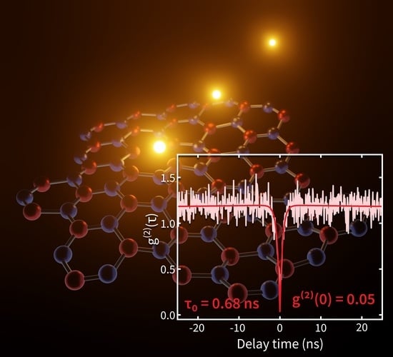
Photodynamics of Bright Subnanosecond Emission from Pure Single-Photon Sources in Hexagonal Boron Nitride
 , ,
, ,
Abstract
:
1. Introduction
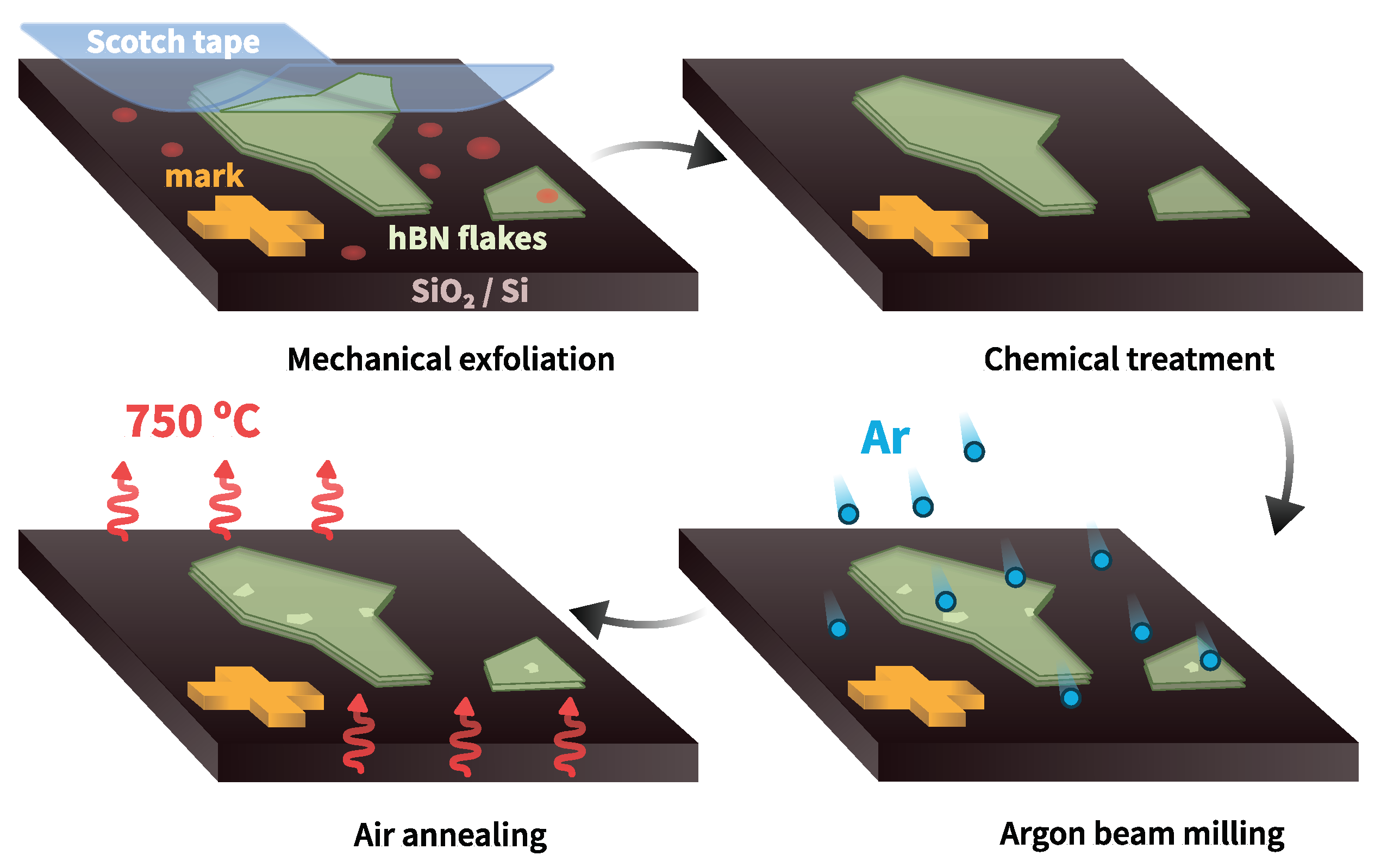
2. Materials and Methods
3. Results and Discussions
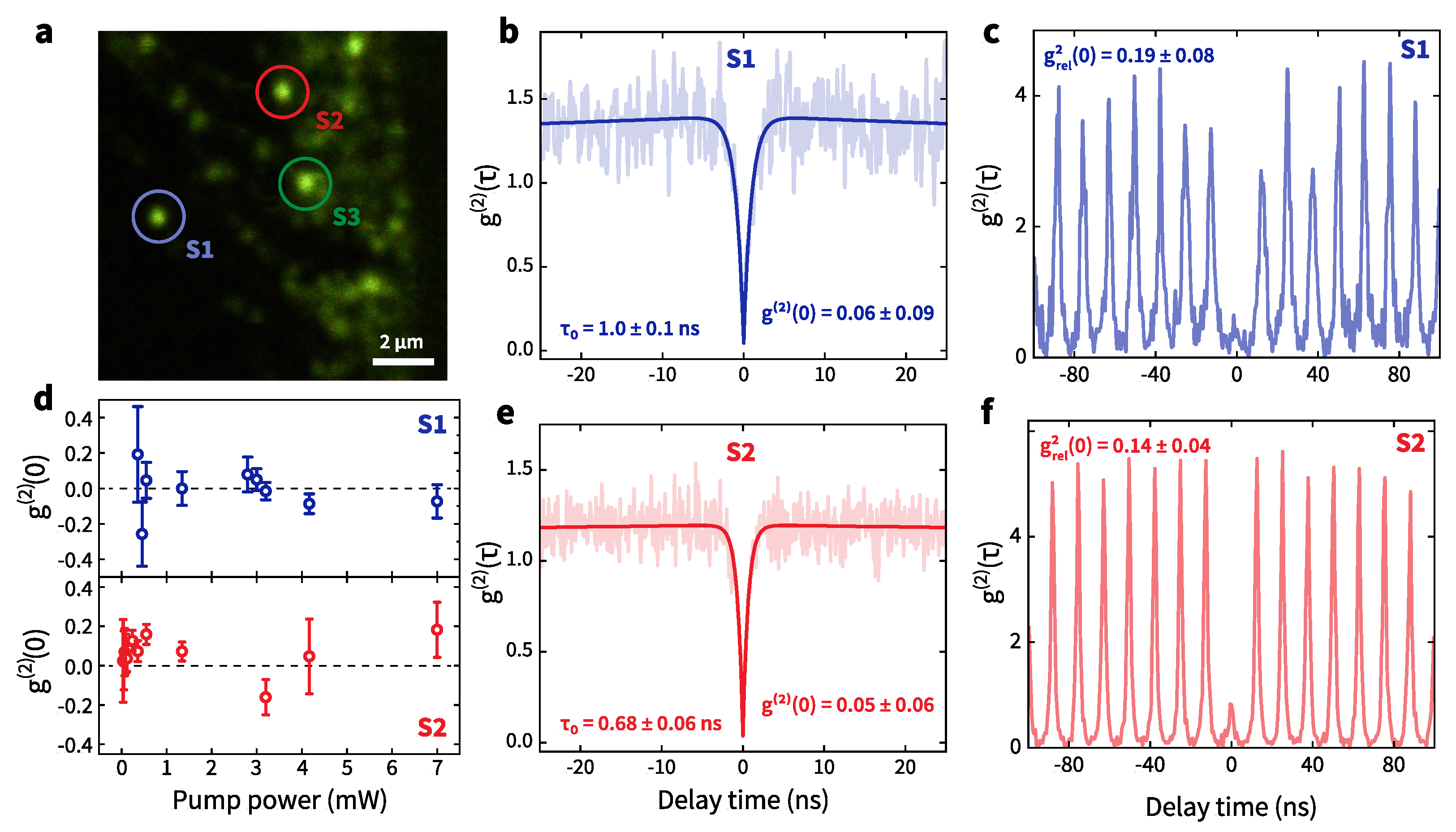
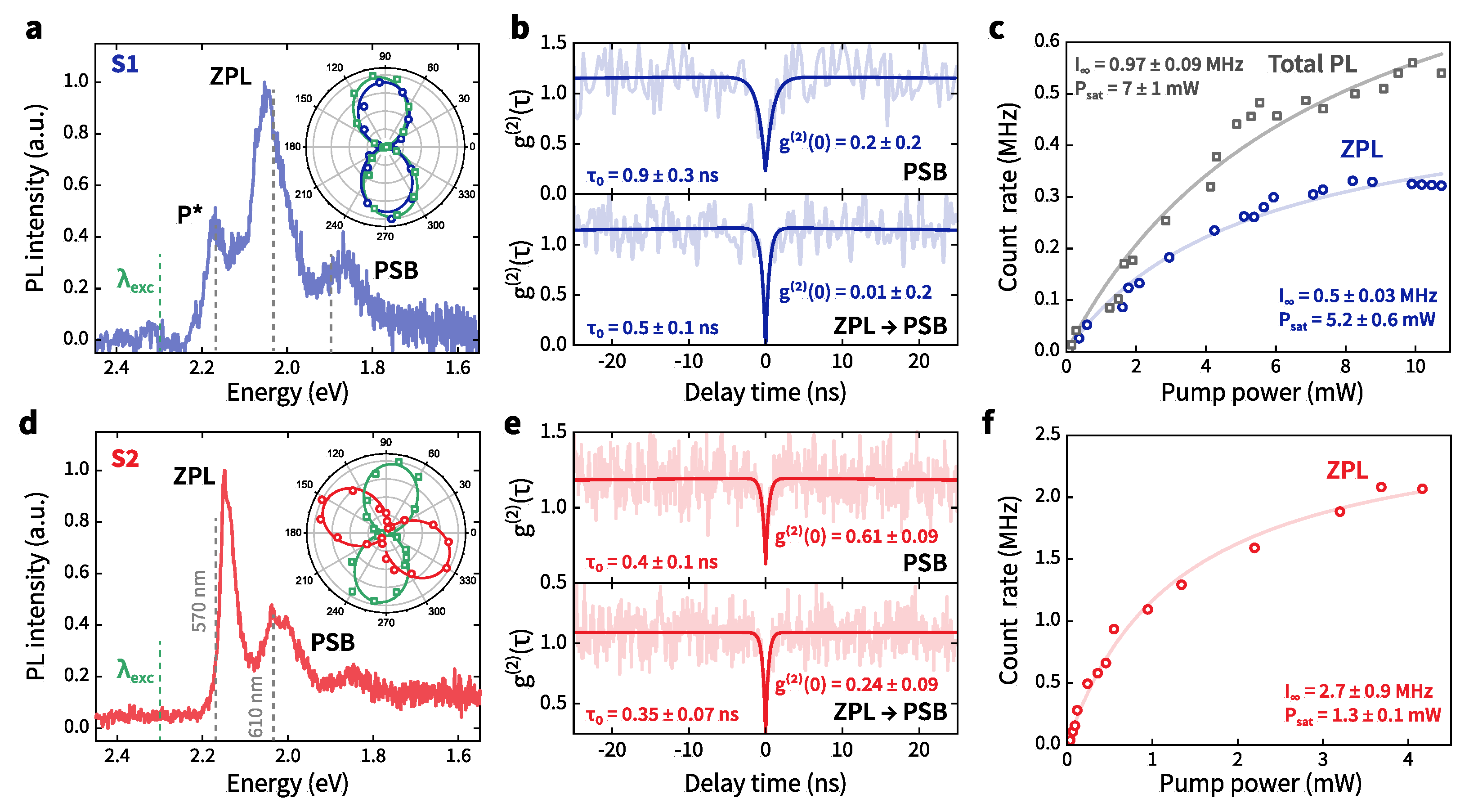
3.1. SPE Identification
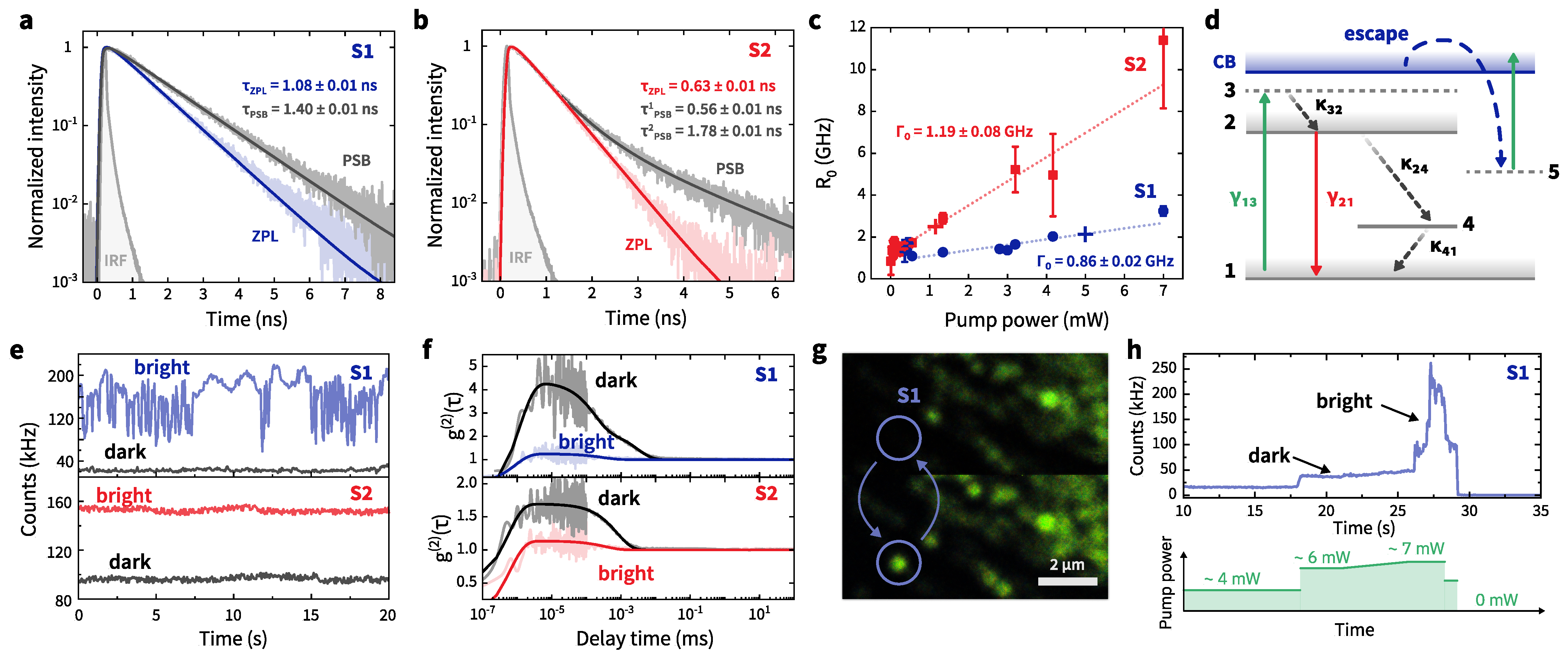
3.2. Photoswitching
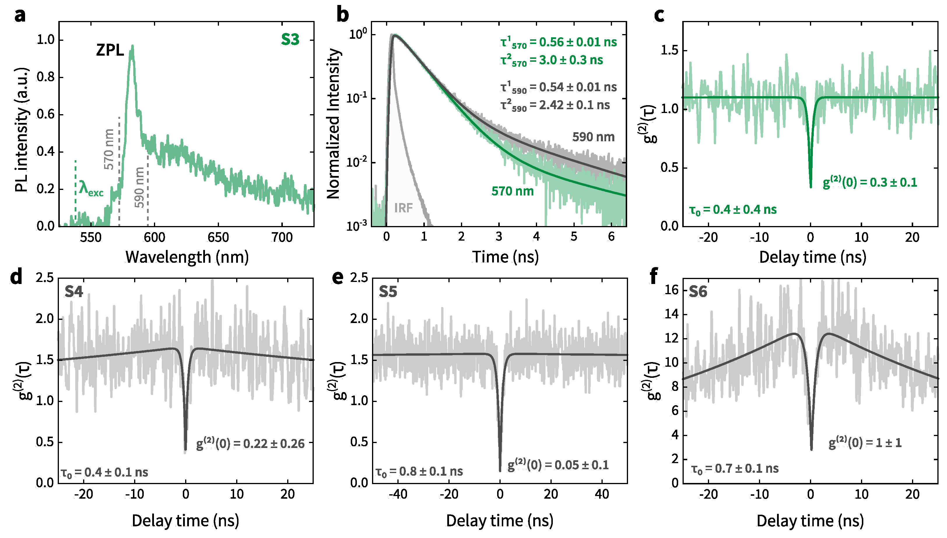
3.3. Defects Nature
4. Conclusions
Author Contributions
Funding
Institutional Review Board Statement
Informed Consent Statement
Data Availability Statement
Acknowledgments
Conflicts of Interest
Abbreviations
| hBN | hexagonal boron nitride |
| SPE | single photon emitter |
| AFM | atomic force microscopy |
| ZPL | zero-phonon line |
| PL | photoluminescence |
| CW | continuous wave |
| HBT | Hanbury Brown-Twiss |
| IRF | instrument response function |
| PSB | phonon sideband |
| TCSPC | time-correlated single photon counting |
| CB | conduction band |
| DB | dangling bond |
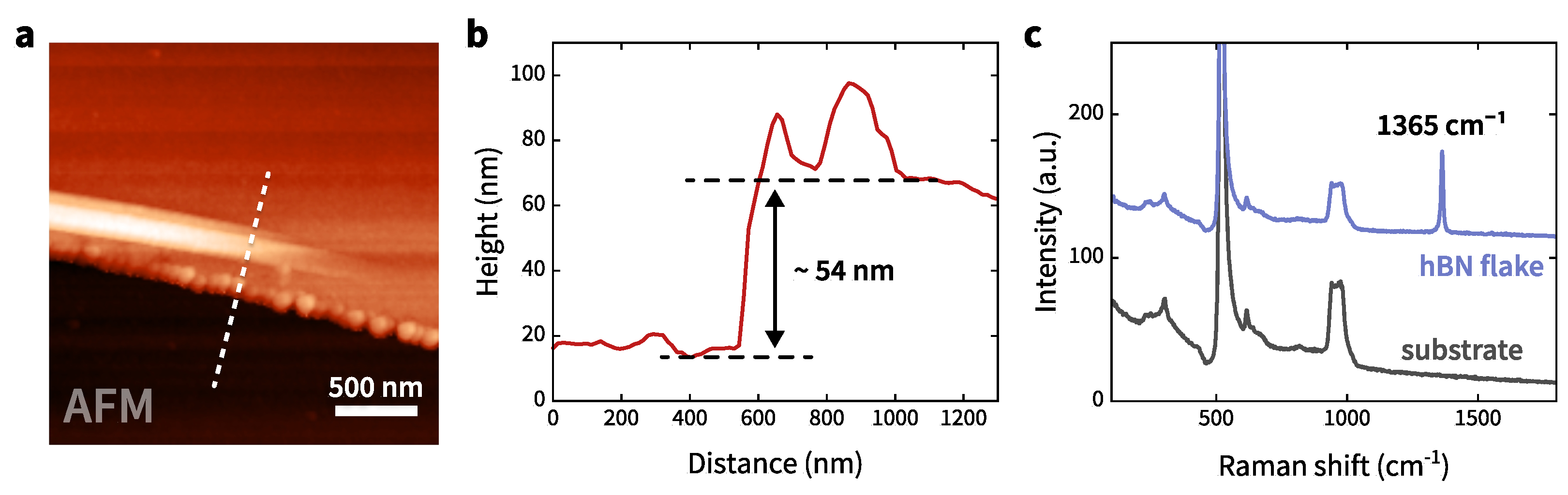
Appendix A. hBN Flake Morphology

Appendix B. Extra Emitters

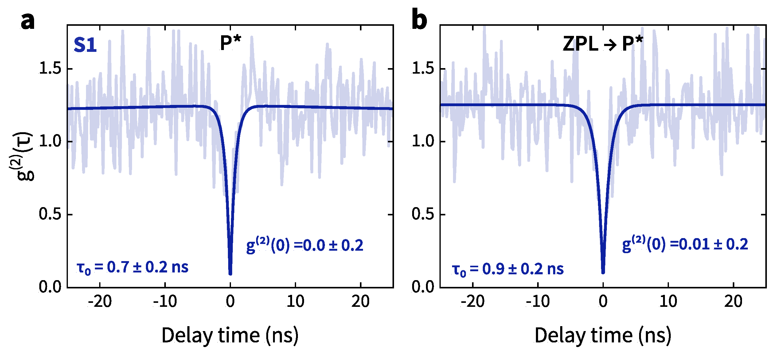
Appendix C. Autocorrelations for P*-Line of S1 Emitter

Appendix D. Photon Autocorrelation Simulation
References
- Aharonovich, I.; Englund, D.; Toth, M. Solid-state single-photon emitters. Nat. Photonics 2016, 10, 631–641. [Google Scholar] [CrossRef]
- Zeng, H.Z.J.; Ngyuen, M.A.P.; Ai, X.; Bennet, A.; Solnstev, A.S.; Laucht, A.; Al-Juboori, A.; Toth, M.; Mildren, R.P.; Malaney, R.; et al. Integrated room temperature single-photon source for quantum key distribution. Opt. Lett. 2022, 47, 1673–1676. [Google Scholar] [CrossRef] [PubMed]
- Zhong, H.S.; Wang, H.; Deng, Y.H.; Chen, M.C.; Peng, L.C.; Luo, Y.H.; Qin, J.; Wu, D.; Ding, X.; Hu, Y.; et al. Quantum computational advantage using photons. Science 2020, 370, 1460–1463. [Google Scholar] [CrossRef] [PubMed]
- Wang, Q.; Zheng, Y.; Zhai, C.; Li, X.; Gong, Q.; Wang, J. Chip-based quantum communications. J. Semicond. 2021, 42, 091901. [Google Scholar] [CrossRef]
- Arakawa, Y.; Holmes, M.J. Progress in quantum-dot single photon sources for quantum information technologies: A broad spectrum overview. Appl. Phys. Rev. 2020, 7, 021309. [Google Scholar] [CrossRef]
- Lukishova, S.G.; Bissell, L.J. Nanophotonic advances for room-temperature single-photon sources. In Quantum Photonics: Pioneering Advances and Emerging Applications; Springer: Berlin/Heidelberg, Germany, 2019; pp. 103–178. [Google Scholar]
- Castelletto, S.; Inam, F.A.; Sato, S.i.; Boretti, A. Hexagonal boron nitride: A review of the emerging material platform for single-photon sources and the spin–photon interface. Beilstein J. Nanotechnol. 2020, 11, 740–769. [Google Scholar] [CrossRef]
- Vasiliev, R.B.; Sokolikova, M.; Vitukhnovskii, A.G.; Ambrozevich, S.; Selyukov, A.; Lebedev, V.S. Optics of colloidal quantum-confined CdSe nanoscrolls. Quantum Electron. 2015, 45, 853. [Google Scholar] [CrossRef]
- Grosso, G.; Moon, H.; Lienhard, B.; Ali, S.; Efetov, D.K.; Furchi, M.M.; Jarillo-Herrero, P.; Ford, M.J.; Aharonovich, I.; Englund, D. Tunable and high-purity room temperature single-photon emission from atomic defects in hexagonal boron nitride. Nat. Commun. 2017, 8, 1–8. [Google Scholar] [CrossRef] [Green Version]
- Boll, M.K.; Radko, I.P.; Huck, A.; Andersen, U.L. Photophysics of quantum emitters in hexagonal boron-nitride nano-flakes. Opt. Express 2020, 28, 7475–7487. [Google Scholar] [CrossRef]
- Nikolay, N.; Mendelson, N.; Özelci, E.; Sontheimer, B.; Böhm, F.; Kewes, G.; Toth, M.; Aharonovich, I.; Benson, O. Direct measurement of quantum efficiency of single-photon emitters in hexagonal boron nitride. Optica 2019, 6, 1084–1088. [Google Scholar] [CrossRef]
- Kubanek, A. Coherent Quantum Emitters in Hexagonal Boron Nitride. Adv. Quantum Technol. 2022, 5, 2200009. [Google Scholar] [CrossRef]
- Shtansky, D.V.; Matveev, A.T.; Permyakova, E.S.; Leybo, D.V.; Konopatsky, A.S.; Sorokin, P.B. Recent Progress in Fabrication and Application of BN Nanostructures and BN-Based Nanohybrids. Nanomaterials 2022, 12, 2810. [Google Scholar] [CrossRef] [PubMed]
- Chen, Y.; Li, C.; White, S.; Nonahal, M.; Xu, Z.Q.; Watanabe, K.; Taniguchi, T.; Toth, M.; Tran, T.T.; Aharonovich, I. Generation of High-Density Quantum Emitters in High-Quality, Exfoliated Hexagonal Boron Nitride. Acs Appl. Mater. Interfaces 2021, 13, 47283–47292. [Google Scholar] [CrossRef] [PubMed]
- Mendelson, N.; Chugh, D.; Reimers, J.R.; Cheng, T.S.; Gottscholl, A.; Long, H.; Mellor, C.J.; Zettl, A.; Dyakonov, V.; Beton, P.H.; et al. Identifying carbon as the source of visible single-photon emission from hexagonal boron nitride. Nat. Mater. 2021, 20, 321–328. [Google Scholar] [CrossRef]
- Xu, X.; Martin, Z.O.; Sychev, D.; Lagutchev, A.S.; Chen, Y.P.; Taniguchi, T.; Watanabe, K.; Shalaev, V.M.; Boltasseva, A. Creating quantum emitters in hexagonal boron nitride deterministically on chip-compatible substrates. Nano Lett. 2021, 21, 8182–8189. [Google Scholar] [CrossRef]
- Gan, L.; Zhang, D.; Zhang, R.; Zhang, Q.; Sun, H.; Li, Y.; Ning, C.Z. Large-Scale, High-Yield Laser Fabrication of Bright and Pure Single-Photon Emitters at Room Temperature in Hexagonal Boron Nitride. ACS Nano 2022, 16, 14254–14261. [Google Scholar] [CrossRef]
- Ziegler, J.; Klaiss, R.; Blaikie, A.; Miller, D.; Horowitz, V.R.; Alemán, B.J. Deterministic quantum emitter formation in hexagonal boron nitride via controlled edge creation. Nano Lett. 2019, 19, 2121–2127. [Google Scholar] [CrossRef]
- Glushkov, E.; Macha, M.; Rath, E.; Navikas, V.; Ronceray, N.; Cheon, C.Y.; Ahmed, A.; Avsar, A.; Watanabe, K.; Taniguchi, T.; et al. Engineering optically active defects in hexagonal boron nitride using focused ion beam and water. ACS Nano 2022, 16, 3695–3703. [Google Scholar] [CrossRef]
- Kumar, A.; Cholsuk, C.; Zand, A.; Mishuk, M.N.; Matthes, T.; Eilenberger, F.; Suwanna, S.; Vogl, T. Localized creation of yellow single photon emitting carbon complexes in hexagonal boron nitride. arXiv 2022, arXiv:2208.13488. [Google Scholar]
- Tawfik, S.A.; Ali, S.; Fronzi, M.; Kianinia, M.; Tran, T.T.; Stampfl, C.; Aharonovich, I.; Toth, M.; Ford, M.J. First-principles investigation of quantum emission from hBN defects. Nanoscale 2017, 9, 13575–13582. [Google Scholar] [CrossRef] [Green Version]
- Abdi, M.; Chou, J.P.; Gali, A.; Plenio, M.B. Color centers in hexagonal boron nitride monolayers: A group theory and ab initio analysis. ACS Photonics 2018, 5, 1967–1976. [Google Scholar] [CrossRef]
- Xu, Z.Q.; Elbadawi, C.; Tran, T.T.; Kianinia, M.; Li, X.; Liu, D.; Hoffman, T.B.; Nguyen, M.; Kim, S.; Edgar, J.H.; et al. Single photon emission from plasma treated 2D hexagonal boron nitride. Nanoscale 2018, 10, 7957–7965. [Google Scholar] [CrossRef] [PubMed] [Green Version]
- Vogl, T.; Doherty, M.W.; Buchler, B.C.; Lu, Y.; Lam, P.K. Atomic localization of quantum emitters in multilayer hexagonal boron nitride. Nanoscale 2019, 11, 14362–14371. [Google Scholar] [CrossRef] [PubMed] [Green Version]
- Fröch, J.E.; Li, C.; Chen, Y.; Toth, M.; Kianinia, M.; Kim, S.; Aharonovich, I. Purcell Enhancement of a Cavity-Coupled Emitter in Hexagonal Boron Nitride. Small 2022, 18, 2104805. [Google Scholar] [CrossRef] [PubMed]
- Selyukov, A.; Danilkin, M.; Eliseev, S.P.; Kuznetsov, A.S.; Grafova, V.P.; Klimonsky, S.O.; Vainer, Y.G.; Vasiliev, R.B.; Vitukhnovsky, A.G. Luminescence relaxation dynamics for planar and rolled-up CdSe nanocrystals in a photonic-crystal matrix. Quantum Electron. 2020, 50, 252. [Google Scholar] [CrossRef]
- Vogl, T.; Lecamwasam, R.; Buchler, B.C.; Lu, Y.; Lam, P.K. Compact cavity-enhanced single-photon generation with hexagonal boron nitride. ACS Photonics 2019, 6, 1955–1962. [Google Scholar] [CrossRef] [Green Version]
- Gritsienko, A.; Kurochkin, N.; Vitukhnovsky, A.; Selyukov, A.; Taydakov, I.; Eliseev, S. Radiative characteristics of nanopatch antennas based on plasmonic nanoparticles of various geometry and tris (2, 2’-bipyridine) ruthenium (II) hexafluorophosphate. J. Phys. D Appl. Phys. 2019, 52, 325107. [Google Scholar] [CrossRef]
- Parto, K.; Azzam, S.I.; Lewis, N.; Patel, S.D.; Umezawa, S.; Watanabe, K.; Taniguchi, T.; Moody, G. Cavity-Enhanced 2D Material Quantum Emitters Deterministically Integrated with Silicon Nitride Microresonators. arXiv 2022, arXiv:2206.14845. [Google Scholar] [CrossRef]
- Grevtseva, I.G.; Ovchinnikov, O.V.; Smirnov, M.S.; Perepelitsa, A.S.; Chevychelova, T.A.; Derepko, V.N.; Osadchenko, A.V.; Selyukov, A.S. The structural and luminescence properties of plexcitonic structures based on Ag 2 S/l-Cys quantum dots and Au nanorods. RSC Adv. 2022, 12, 6525–6532. [Google Scholar] [CrossRef]
- Kianinia, M.; Bradac, C.; Sontheimer, B.; Wang, F.; Tran, T.T.; Nguyen, M.; Kim, S.; Xu, Z.Q.; Jin, D.; Schell, A.W.; et al. All-optical control and super-resolution imaging of quantum emitters in layered materials. Nat. Commun. 2018, 9, 1–8. [Google Scholar] [CrossRef] [Green Version]
- Noh, G.; Choi, D.; Kim, J.H.; Im, D.G.; Kim, Y.H.; Seo, H.; Lee, J. Stark tuning of single-photon emitters in hexagonal boron nitride. Nano Lett. 2018, 18, 4710–4715. [Google Scholar] [CrossRef] [PubMed]
- Klokov, A.Y.; Frolov, N.Y.; Sharkov, A.I.; Nikolaev, S.N.; Chernopitssky, M.A.; Chentsov, S.I.; Pugachev, M.V.; Duleba, A.I.; Shupletsov, A.V.; Krivobok, V.S.; et al. 3D Hypersound Microscopy of van der Waals Heterostructures. Nano Lett. 2022, 22, 2070–2076. [Google Scholar] [CrossRef] [PubMed]
- Pugachev, M.V.; Duleba, A.I.; Galiullin, A.A.; Kuntsevich, A.Y. Micromask lithography for cheap and fast 2D materials microstructures fabrication. Micromachines 2021, 12, 850. [Google Scholar] [CrossRef] [PubMed]
- Li, C.; Xu, Z.Q.; Mendelson, N.; Kianinia, M.; Toth, M.; Aharonovich, I. Purification of single-photon emission from hBN using post-processing treatments. Nanophotonics 2019, 8, 2049–2055. [Google Scholar] [CrossRef] [Green Version]
- Gritsienko, A.V.; Matveev, A.T.; Kurochkin, N.S.; Voskanyan, G.R.; Shcherbakov, D.A.; Shtansky, D.V.; Vitukhnovsky, A.G. Photocontrol of Single-Photon Generation in Boron Nitride Nanoparticles: Implications for Quantum Photon Sources, Sub-Diffraction Nanoscopy, and Bioimaging. ACS Appl. Nano Mater. 2022, 5, 10462–10470. [Google Scholar] [CrossRef]
- Gritsienko, A.; Kurochkin, N.; Lega, P.; Orlov, A.; Ilin, A.; Eliseev, S.; Vitukhnovsky, A. Hybrid cube-in-cup nanoantenna: Towards ordered photonics. Nanotechnology 2021, 33, 015201. [Google Scholar] [CrossRef]
- Fishman, R.E.; Patel, R.N.; Hopper, D.A.; Huang, T.Y.; Bassett, L.C. Photon emission correlation spectroscopy as an analytical tool for quantum defects. arXiv 2021, arXiv:2111.01252. [Google Scholar]
- Kurochkin, N.; Savinov, S.; Bi, D.; Sychev, V.; Eliseev, S.; Gritsienko, A. Characterization of Milled High-Pressure High-Temperature NV-Center Nanodiamonds for Single-Photon Source Applications. J. Russ. Laser Res. 2021, 42, 713–720. [Google Scholar] [CrossRef]
- Tran, T.T.; Zachreson, C.; Berhane, A.M.; Bray, K.; Sandstrom, R.G.; Li, L.H.; Taniguchi, T.; Watanabe, K.; Aharonovich, I.; Toth, M. Quantum emission from defects in single-crystalline hexagonal boron nitride. Phys. Rev. Appl. 2016, 5, 034005. [Google Scholar] [CrossRef] [Green Version]
- Tran, T.T.; Elbadawi, C.; Totonjian, D.; Lobo, C.J.; Grosso, G.; Moon, H.; Englund, D.R.; Ford, M.J.; Aharonovich, I.; Toth, M. Robust multicolor single photon emission from point defects in hexagonal boron nitride. ACS Nano 2016, 10, 7331–7338. [Google Scholar] [CrossRef]
- Exarhos, A.L.; Hopper, D.A.; Grote, R.R.; Alkauskas, A.; Bassett, L.C. Optical signatures of quantum emitters in suspended hexagonal boron nitride. ACS Nano 2017, 11, 3328–3336. [Google Scholar] [CrossRef] [PubMed] [Green Version]
- Kozawa, D.; Rajan, A.G.; Li, S.X.; Ichihara, T.; Koman, V.B.; Zeng, Y.; Kuehne, M.; Iyemperumal, S.K.; Silmore, K.S.; Parviz, D.; et al. Observation and spectral assignment of a family of hexagonal boron nitride lattice defects. arXiv 2019, arXiv:1909.11738. [Google Scholar]
- Vogl, T.; Campbell, G.; Buchler, B.C.; Lu, Y.; Lam, P.K. Fabrication and deterministic transfer of high-quality quantum emitters in hexagonal boron nitride. ACS Photonics 2018, 5, 2305–2312. [Google Scholar] [CrossRef]
- Patel, R.N.; Hopper, D.A.; Gusdorff, J.A.; Turiansky, M.E.; Huang, T.Y.; Fishman, R.E.K.; Porat, B.; Van de Walle, C.G.; Bassett, L.C. Probing the Optical Dynamics of Quantum Emitters in Hexagonal Boron Nitride. PRX Quantum 2022, 3, 030331. [Google Scholar] [CrossRef]
- Feldman, M.A.; Puretzky, A.; Lindsay, L.; Tucker, E.; Briggs, D.P.; Evans, P.G.; Haglund, R.F.; Lawrie, B.J. Phonon-induced multicolor correlations in hBN single-photon emitters. Phys. Rev. B 2019, 99, 020101. [Google Scholar] [CrossRef] [Green Version]
- Feldman, M.A.; Marvinney, C.E.; Puretzky, A.A.; Lawrie, B.J. Evidence of photochromism in a hexagonal boron nitride single-photon emitter. Optica 2021, 8, 1–5. [Google Scholar] [CrossRef]
- Jungwirth, N.R.; Fuchs, G.D. Optical absorption and emission mechanisms of single defects in hexagonal boron nitride. Phys. Rev. Lett. 2017, 119, 057401. [Google Scholar] [CrossRef] [Green Version]
- White, S.J.; Yang, T.; Dontschuk, N.; Li, C.; Xu, Z.Q.; Kianinia, M.; Stacey, A.; Toth, M.; Aharonovich, I. Electrical control of quantum emitters in a Van der Waals heterostructure. Light. Sci. Appl. 2022, 11, 1–9. [Google Scholar] [CrossRef] [PubMed]
- Khatri, P.; Ramsay, A.J.; Malein, R.N.E.; Chong, H.M.; Luxmoore, I.J. Optical gating of photoluminescence from color centers in hexagonal boron nitride. Nano Lett. 2020, 20, 4256–4263. [Google Scholar] [CrossRef]
- Katsaba, A.; Fedyanin, V.; Ambrozevich, S.; Vitukhnovsky, A.; Lobanov, A.; Selyukov, A.; Vasiliev, R.; Samatov, I.; Brunkov, P. Characterization of defects in colloidal CdSe nanocrystals by the modified thermostimulated luminescence technique. Semiconductors 2013, 47, 1328–1332. [Google Scholar] [CrossRef]
- Turiansky, M.E.; Alkauskas, A.; Bassett, L.C.; Van de Walle, C.G. Dangling bonds in hexagonal boron nitride as single-photon emitters. Phys. Rev. Lett. 2019, 123, 127401. [Google Scholar] [CrossRef] [PubMed] [Green Version]
- Turiansky, M.E.; Van de Walle, C.G. Boron dangling bonds in a monolayer of hexagonal boron nitride. J. Appl. Phys. 2021, 129, 064301. [Google Scholar] [CrossRef]
- Turiansky, M.E.; Van de Walle, C.G. Impact of dangling bonds on properties of h-BN. 2D Mater. 2021, 8, 024002. [Google Scholar] [CrossRef]
- Scavuzzo, A.; Mangel, S.; Park, J.H.; Lee, S.; Loc Duong, D.; Strelow, C.; Mews, A.; Burghard, M.; Kern, K. Electrically tunable quantum emitters in an ultrathin graphene–hexagonal boron nitride van der Waals heterostructure. Appl. Phys. Lett. 2019, 114, 062104. [Google Scholar] [CrossRef]
- McDougall, N.L.; Partridge, J.G.; Nicholls, R.J.; Russo, S.P.; McCulloch, D.G. Influence of point defects on the near edge structure of hexagonal boron nitride. Phys. Rev. B 2017, 96, 144106. [Google Scholar] [CrossRef]
- Chen, Y.; Quek, S.Y. Photophysical Characteristics of Boron Vacancy-Derived Defect Centers in Hexagonal Boron Nitride. J. Phys. Chem. C 2021, 125, 21791–21802. [Google Scholar] [CrossRef]
- Li, K.; Smart, T.; Ping, Y. C2CN as a 2 eV Single-Photon Emitter Candidate in Hexagonal Boron Nitride. arXiv 2021, arXiv:2110.01787. [Google Scholar]
- Wein, S.; Lauk, N.; Ghobadi, R.; Simon, C. Feasibility of efficient room-temperature solid-state sources of indistinguishable single photons using ultrasmall mode volume cavities. Phys. Rev. B 2018, 97, 205418. [Google Scholar] [CrossRef]


| (GHz) | (GHz) | (MHz) | (MHz) | (MHz) | (MHz) | |
|---|---|---|---|---|---|---|
| S1 (bright state) | 0.27 | 0.88 | 2.7 | 2.6 | - | - |
| S1 (dark state) | 0.13 | 0.7 | 16.5 | 3.2 | 2.3 | 1.4 |
| S2 (bright state) | 0.11 | 1.5 | 4.9 | 2.5 | - | - |
| S2 (dark state) | 0.93 | 1.7 | 10 | 0.7 | - | - |
Publisher’s Note: MDPI stays neutral with regard to jurisdictional claims in published maps and institutional affiliations. |
© 2022 by the authors. Licensee MDPI, Basel, Switzerland. This article is an open access article distributed under the terms and conditions of the Creative Commons Attribution (CC BY) license (https://creativecommons.org/licenses/by/4.0/).
Share and Cite
Gritsienko, A.V.; Duleba, A.; Pugachev, M.V.; Kurochkin, N.S.; Vlasov, I.I.; Vitukhnovsky, A.G.; Kuntsevich, A.Y. Photodynamics of Bright Subnanosecond Emission from Pure Single-Photon Sources in Hexagonal Boron Nitride. Nanomaterials 2022, 12, 4495. https://doi.org/10.3390/nano12244495
Gritsienko AV, Duleba A, Pugachev MV, Kurochkin NS, Vlasov II, Vitukhnovsky AG, Kuntsevich AY. Photodynamics of Bright Subnanosecond Emission from Pure Single-Photon Sources in Hexagonal Boron Nitride. Nanomaterials. 2022; 12(24):4495. https://doi.org/10.3390/nano12244495
Chicago/Turabian StyleGritsienko, Alexander V., Aliaksandr Duleba, Mikhail V. Pugachev, Nikita S. Kurochkin, Igor I. Vlasov, Alexei G. Vitukhnovsky, and Alexandr Yu. Kuntsevich. 2022. "Photodynamics of Bright Subnanosecond Emission from Pure Single-Photon Sources in Hexagonal Boron Nitride" Nanomaterials 12, no. 24: 4495. https://doi.org/10.3390/nano12244495